Unit – II
Theory of p-n junction Diode
Diode Current Equation
 Ampiers
Where,
V= Applied voltage across the diode in volts
I=Current flow through the diode in amperes.
n= 2 for silicon P-N junction diode
=1 for germanium P-N junction diode.
IO = reverse saturation current flow through diode in amperes.
VT =Is the voltage equivalent of temperature in volts.
VT= K X T volt’s
K=Boltzmann’s constant
K=8.62 * 10 -s ev/k
I= temperature in ok
The equation VI= K * T indicates that the current flow through the diode also depend upon the ambient temperature.
Room temperature =25 0c
T= 273+25=298K
VT=K * T


Static or DC Resistance
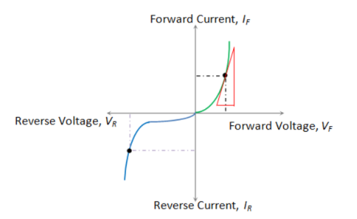
It is the resistance offered by the diode to the flow of DC through it when we apply a DC voltage to it. Mathematically the static resistance is expressed as the ratio of DC voltage applied across the diode terminals to the DC flowing through it (shown by the black dotted line in Figure) i.e.
Dynamic or AC Resistance
It is the resistance offered by the diode to the flow of AC through it when we connect it in a circuit which has an AC voltage source as an active circuit element. Mathematically the dynamic resistance is given as the ratio of change in voltage applied across the diode to the resulting change in the current flowing through it. This is shown by the slope-indicating red solid lines in Figure and is expressed as
Transition Capacitance
When the diode is reversed biased the majority carriers’ move away from junction as the width of depletion layer increases. Due to the immobile carriers on both the sides a capacitance is developed CT.
CT = | |
|
The voltage change dV in time dt gives current i
i =  = CT
= CT
When reverse bias increases the width of depletion region increases and the transition capacitance decreases.
CT for step graded junction:
CT = 
W2 =  [
[ +
+  ]
]
W = [ ]2
]2
CT= A (  )1/2 x (
 )1/2
)1/2
CT in linear graded junction
CT = 
W = [ ]1/2
]1/2
CT= A (  )1/2 x (
 )1/2
)1/2
Diffusion Capacitance or Storage Capacitance CD
In forward biased the potential barrier at the junction decreases. As a result, holes get injected from the P-side to the N-side and electron gets injected from the N-side to the P-side. These injected charges get stored near the junction just outside the depletion layer, holes in the N-region and electrons in the P-region. Due to charge storage, the voltage lags behind the current producing the capacitance effect. Such a capacitance is called diffusion capacitance or storage capacitance CD
CD = 
I = 
 = mean life time of hole
Q = stored charge
Tp = 
LP = diffusion length of holes
Dp= Diffusion constant for holes
CD =  =
= 
CD = 
For forward diode CD as well as CT are present but CD>>CT. Hence CT can be neglected
For reverse bias CT>>CD. Hence CD can be neglected.
As we already know the working of p-n junction diode. As the temperature increases the covalent bond are broken which releases many electrons and protons. This increases the amount of current flow in the diode. The diode characteristics are shown below
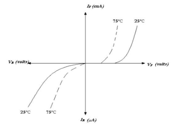
The above characteristics clearly shows that the forward characteristics are shifted upwards and reverse characteristics are shifted downwards with increase in temperature.
Whenever a specified voltage is exceeded, the diode resistance gets increased, making the diode reverse biased and it acts as an open switch. Whenever the voltage applied is below the reference voltage, the diode resistance gets decreased, making the diode forward biased, and it acts as a closed switch.
The following circuit explains the diode acting as a switch.

A switching diode has a PN junction in which P-region is lightly doped and N-region is heavily doped. The above circuit symbolizes that the diode gets ON when positive voltage forward biases the diode and it gets OFF when negative voltage reverse biases the diode.
As the forward current flows till then, with a sudden reverse voltage, the reverse current flows for an instance rather than getting switched OFF immediately. The higher the leakage current, the greater the loss. The flow of reverse current when diode is reverse biased suddenly, may sometimes create few oscillations, called as RINGING.
This ringing condition is a loss and hence should be minimized. To do this, the switching times of the diode should be understood.
To analyse the diode in transition region between the non-conducting and full conducting the piecewise linear model is used. It approximates the true linear behaviour of diode. The circuit is shown below.

The diode is replaced with components that are more compatible with standard circuits. A battery with a resistor is added in the circuit. When diode is conducting the resistor creates a linear relationship between forward a voltage and forward current.
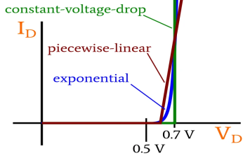
The point from where curve departs can be adjusted by changing the voltage of battery.
Zener Breakdown: - This type of breakdown occurs in heavily doped P-N junction in which the depletion region is very narrow.
All the applied reverse voltage appears across the depletion layer. The electric field is vtg per unit distance. It is very intense at the depletion region.
There for it can pull the electronic out of the valance bond by breaking the covalent bonds and producing the free electrons. This process is known as zener effect.
Due to this heavy current flow & diode may damage.
Zener Diode
- Zener diode is a special type of p-n junction semiconductor diode in this diode the reverse breakdown voltage is adjusted precisely between 3v to 200v.
- Its applications are based on this principle hence Zener diode is called as a breakdown diode.
- The doping level of the imparity added to manufacture the zener diode is controlled in order to adjust the precise value of breakdown voltage.
PRINCIPLE OF OPERATION: - A zener diode can be forward biased or reverses biased. Its operation in the forward biased mode is same as that of a p-n junction diode but its operation in the reverse biased mode is sustainably deferent.


Numerical:
A 5.0V stabilized power supply is required to be produced from a 12V DC power supply input source. The maximum power rating PZ of the zener diode is 2W. Using the zener regulator circuit above calculate:
a). The maximum current flowing through the zener diode.
Maximum current = Watts/ Voltage =2W/5V =400mA
b). The minimum value of the series resistor, RS
 = 17.5 Ω
c). The load current IL if a load resistor of 1kΩ is connected across the zener diode.

d). The zener current IZ at full load.
Iz =Is -Il =440mA – 5mA = 395mA
Varacter Diode
The diode whose internal capacitance varies with the reverse voltage are known as varactor diodes. They work only in reverse bias. They are used where variable capacitance is required.
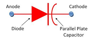
As the diode operates only in reverse bias the width of depletion region increases and hence the current decreases. It is used as a charge storing device.
The transition capacitanceCT = 
In reverse bias the width of depletion region increases and hence the capacitance decreases. The VI characteristics shows the same

Tunnel Diode
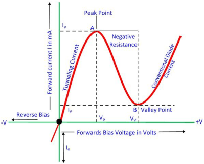
It is a heavily doped p-n junction diode in which the electric current flows due to tunnelling. The germanium metal is used in tunnel diode. As they are heavily doped with impurities, they are negative resistance device. The current across the diode decrease with increase in voltage.
Tunnelling Effect:
This means penetration of electrons from small depletion region from n-side conduction band to p-side valence band. The width of depletion region depends on the impurities added less the number of impurities added wider the depletion region and vice versa.
As the tunnel diodes are heavily doped so they have narrow depletion region. There is built-in potential in this narrow depletion region. This electric field in the depletion region exerts electric force in a direction opposite to that of the external electric field.

In tunnel diode the VB and CB energy in n type are lower than the p type and dure to narrow depletion region the electrons directly tunnel across this small depletion region from n-side CB to p-side VB.
Tunnel diode characteristics:
When the applied potential is increased the current increases to some extent. After the voltage is increased more the tunnel current reaches its maximum value as the energy level of CB and VB overlap and maximum electrons flow from n-side to p-side. If the voltage is increased further there is misalignment in the CB and VB resulting is small current flow. When voltage is largely increased the tunneling current decreases as the VB and CB do not overlap each other now. If this applied voltage is greater than the built-in potential of the depletion layer, the regular forward current starts flowing through the tunnel diode.
Photodiode
The photodiode is a p-n junction semiconductor diode which is always operated in the reverse biased condition.
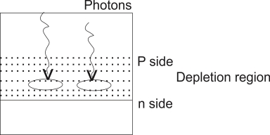
The light is always focused through a glass lens on the junction of the photodiode As the photodiode is reverse biased the depletion region is quite wide, penetrated on both side of the junction.
The photons incident on the depletion region will impact their energy to the Ions present in depletion region and generates e hole pairs.
The photons incident on the depletion region so the number of electron hole pairs will be generated depends on the intensity of light [number of photons] These and holes will be attracted towards the +ve& -ve terminals respectively of the photo current ,
With increase in the light intensity more number of e hole pairs are generated and the photo current increases thus the photocurrent is proportional to the light intensity.
Light Emitting Diodes
An LED emits light when electrical energy is applied to it. For proper operation it is necessary to forward bias the LED.
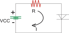
Construction of LED :-
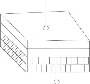
To make emission of light in one direction cup type construction is used for LED.
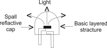
PRINCIPLE LED OPERATION
When the led is forward is forward biased the electrons in the n-region will cross the junction and recombine with the holes in the p- type material.
These free e- reside in the conduction band & hence at a higher energy level than the holes in the valence band
When recombination takes place this e- return peak to the valence band which is at a lower energy level than the conduction band.
While returning back the recombining e-give away the excess energy in the form of light . This process is called as electroluminescence. In this way an LED emits light.
Color of the Emitted Light
Material UseColor ofEmitted Light
i)Gallium Arsenide (GOAS) In fared (IR)
Ii) GaASP(gallium arsenide Red or Yellow
Phosphide)
Iii) Gallium phosphide (GAP) Red or Green
Application
Used in 7 Segment Display
Schottky Barrier Diode
It is unlike normal p-n junction diode because it uses a metal at the junction. The provide extremely low forward voltage and has high speed because it does not use holes. The symbol of Schottky diode is show below.
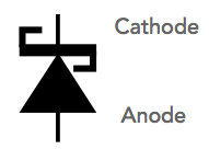
It has low turn on voltage which is 0.2V and 0.3V for silicon Schottky diode. As the active area is very small so it has low capacitance levels.
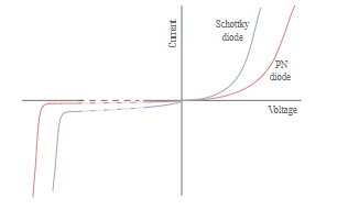
The above characteristics shows the fast performance of this diode.
Uses:
They are used in RF mixer and detector diode. They are uses in power circuits and also as power rectifiers.
Half Wave rectifier
1) Due to the unidirectional current flow through the transformer there is a possibility of core saturation to avoid this transformer size must be increased.
2) Ripple factor is high.
3) Low rectification effecting.
4) Law TUF.
5) Law D.C O/P VTG & current.
6) Large filter component are required.
ADVANTAGES:-
1) Simple Construction.
2) Component required less.
3) Small size.
APPLICATION:-
Walkman, law cost power supply.
TRANSFORMER UTILISATION FACTOR (TUF):-It indicates how well the ilp transformer is being utilized
TUF= DC O/P Power / AC power rating of the transformer

Full Wave Rectifier
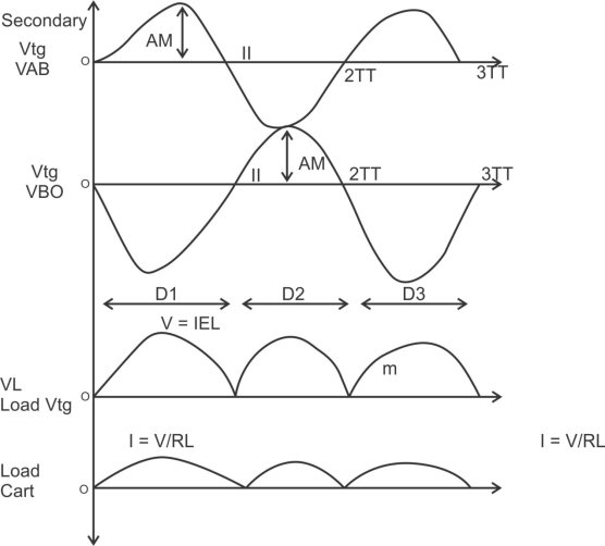
1) A centre tapped rectifier is a type of full wave rectifier that uses two diode connected to the secondary of a centre tapped transformer.
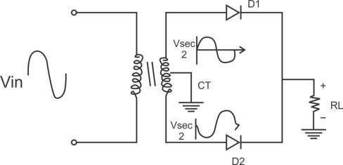
Center tapped full wave rectifier operation:-
I) During positive half cycle of i/p ac supply.
Diagram

D1.Is in forward biased & D2 is in reverse biased.
II)During -ve half cycle.

D1 Reverse biased
D2 Forward biased
ADVANTAGES
1) law ripple factor as Compared to HKR.
2)Better rectification efficiency.
3) Better TUF.
4)Higher value of average load vtg & avg load crt.
5)No possibility of transformer core saturation.
DISADVANTAGES
PIV of diode is 2vm , more size costly.
APPLICATION
I) Battery charges.
2)power supply at laboratory, high current, electronic ckt.
Diode Clipper or Limiting Circuits:
Diode C kts called limiters or clippers are sometimes used to clip off portions of signal voltages above or below certain levels.
Another type of diode ckt called a clamper is used to add or restore a d.c level to an electrical signal.
Below fig a) that limits or clips the positive part of the input voltageAs the ilp vtg goes positive the diode become forward biased Because the cathode is at ground potential (ov)the anode cannot exceed 0.7v (for si)
So point A is limited to 0.7v the diode is reverse biased and appears as an open. The O/P VTG looks like the with a magnitude determined by the voltage divider formed by R1& the load resistor RL.
Vout=(RL/R1+RL) vin
If R1 small compared to RL then vout =vin

Clipper of the positive alternation. The diode is F,B during the +ve alternate RB during –ve alternation:-
Negative Clipper:-

Limiting of the negative alternation the diode is PB during the –ve alternation R.B during the +ve alternation.
During Reverse bias the +ve part of the ilp vtg is clipped off when the diode is forward biased during the –ve part of the ilp vtg is clipped off. When the diode is F.B during the –ve part of the ilp vtg point A is held at 0.7v by the diode is no longer forward biased and a voltage appears across RL proportional to the ilp vtg.
Problem:- What would you expect to see displayed on oscilloscope connected across RL in the Limiter.

The diode is forward biased and conducts when then the i/pvtg goes below -0.7v so for the –ve limiter , the peak o/p vtg across RL can be determined by the following
Equation -
Volt=(RL/R+RL) Vin
=(1k/100+1k)10v
= 1K/1.1K*10
=1*103/1.1*103*10
= 1*104/11*102*10
= 1*104*10-2*10
=10/11 10*10*10/11
Volt=10000/11=9.09V
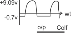
Biased parallel /Clipper:-1) The level to which an act voltage is limited can be adjusted by adding a bias vtg in series with the diode shown in fig.

The voltage at point A mast equal VBINS+0.7v before the diode will become forward biased & conduct
Once the diode begins to conduct the vtg at point A is limited to VBINS +0.7 so that all ilp above this level is clipped off

To limit a vtg to a specified –ve level the diode & bios vtg must be connected. In this case the vtg at point ‘A’ must go below –VBIN-0.7v to forward biased the diode & initiate limiting action
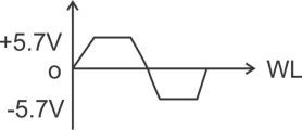
Prob:- fig shows a ckt combing a positive clipper with a-ve clipper .Determine the o/p vtg c/f

When the voltage at point A riches +5.7V diode A conducted and limits the waveform to +5.7v diode D2 does not conduct until the voltage reaches -5.7V
Therefore positive voltages above +5.7V & -vevoltages below -5.7V are clipped off
Diode Clampers:-
1) Positive Clamper:-
Diagram:-

Assumptions :-
1) The V/p is a perfect sine waveform
2)The value of R& C are chosen such that the Line constant T=RC is large equal
3)The diode is an ideal one
4)TheRc time constant is much longer as compared to one cattle period ‘T’ of the input.
RC>100T
Operation :-I n the first negative half cycle after turning on the Ckt the diode acts as a closed S/W & charges the capacitor to peak ilpvtg VM with the polarity shown below

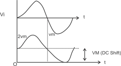
The diode reverse biased in both half cycle so it remains off.
2)Negative Clamper:-

In the first positive half cycle the capacitor will charge through the forward biased to peak vtgvm
The charging takes place very quickly as the diode resistances negligibly small
Once the capacitor charges to vm the diode is reverse biased and stops conducting.

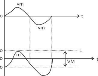
Diagram non ideal diode
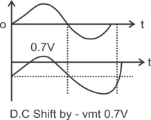
Biased Clamper:-
Diagram:-
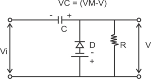
-Clamper with additional dc source:-
Diagram-
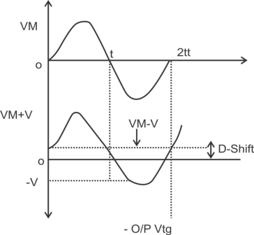
The load vtg W/F shows d.c level shift is positive but less than +vm
Level shift is given by
DG shift=vm-v
Operation:-
In the –ve half cycle ilp the diode will be forward biased and capacitor gets charged to a vtg (vm-v) volts with the polarities shown.
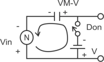
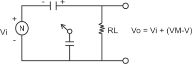
In above diagram during positive half cycle diode will remain permanently off therefore .the job of the diode is only to charge the capacitor.
Vo=vc+vi
Vo=(vm-v)+vi
Series clipper CKT:-
1)Series Negative clipper :- Ideal diode
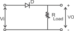
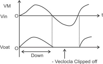
Operation:-
In the positive half cycle of the sinusoidal ilp the diode is forward biased. Being an ideal diode , it acts as a closed switch & connects the load across the ilp the load vtg there fore equal to the ilp vtg in the positive half cycle.
In the –ve half cycle of the diode is reverse biased acts as an open ckts/w the load vtg is therefore zero during the –ve half cycle.
2) Series Positive clipper:-

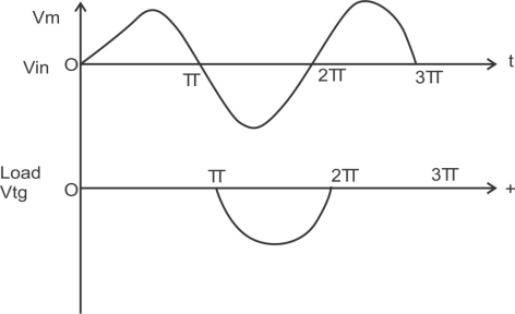
Series clipper with a D.C supply biased [clippers] :-
1) Biased Series – ve Clipper:-
2)


Operation:-
The operation of this ckt can be divided in to there intervals
1) Operation when in is +ve but less than v:-in the positive half cycle of the ilp as long as vin v the diode is not forward biased, therefore from to and then from t2 to t/2 shown in fig below the diode will remain in off state and the o/p voltage will be zero.

Fig -a)Equivalent ckt for +vin>v -
-
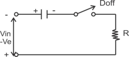
Fig b) Equivalent ckt for vin -ve
References
- S. Salivahanan, N. Suresh Kr. & A. Vallavaraj, ―Electronic Devices & Circuit‖, Tata McGraw Hill,
2008
2. Millman, Halkias and Jit, ―Electronic devices and circuits‖ McGraw Hill
3. Boylestad & Nashelsky, ―Electronic Devices & Circuits‖, Pearson Education, 10TH Edition.
4. Sedra & Smith, ―Micro Electronic Circuits‖ Oxford University Press, VI Edition
5. Robert T. Paynter, ―Introducing Electronic Devices & Circuits‖, Pearson Education, VII Edition, 2006