Unit – IV
Application of BJT
Common Base Configuration
The notation and symbols of pnp and npn transistors are given below:
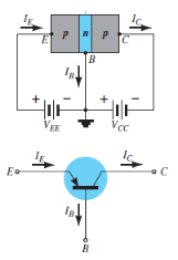
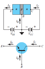
Fig. 4: PNP CB and NPN CB (Ref. 2)
Here the base is common to both the input and output sides of the configuration.
The flow of holes will govern the direction of current.
Hence, Ic = Ib + Ie
Where Ic, Ib, Ie are the collector, base and emitter currents respectively.
The graphical symbol of the PNP common base configuration is
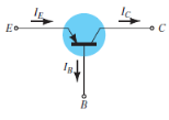
Fig. 5 : PNP common base(Ref. 2)
The arrow in the above symbol shows the direction of emitter current in the device.
Now, to study the behavior of the device we require two characteristics:
Input Characteristic Curve
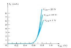
Fig.6: Input Characteristic Curve (Ref. 2)
- It is the relation between the input current IE to the input voltage VBE for various levels of output voltage VCB.
- It is also known as driving point characteristics.
Output Characteristic Curve
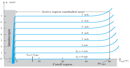
Fig.7 : Output Characteristic Curve (Ref. 2)
- It is the relation between the output current IC to the output voltage VCB for various levels of input current IE.
- It is also known as collector set of characteristics.
- It has three basic regions:
- Active Region
Here, base-emitter junction is forward biased and collector-base junction is reverse biased.
As input current IE increases above zero, output current IC increases to a magnitude equal to IE as determined by the basic transistor current relationship.
So the first approximation determined by the curve is
IC ≈ IE
2. Cut-off Region
It is defined as the region where the collector current IC is equal to 0A.
Here, the base-emitter junction and the collector-base junction both are in reverse bias.
3. Saturation Region
It is the region that lies towards the left of VCB = 0V.
Here, the base-emitter junction and the collector-base junction both are in forward bias.
Common Emitter Configuration
The notation and symbols of npn and pnp transistors are given below:
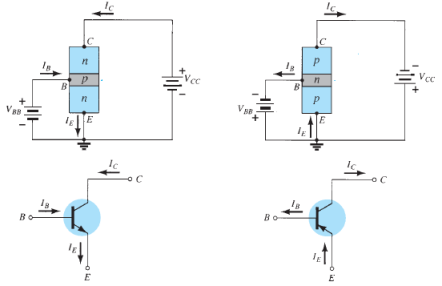
Fig. 8: NPN CE and PNP CE (Ref. 2)
In the above figure all the currents are shown in their actual conventional directions.
The current relation developed earlier is still applicable,
IE = IB + IC
Where IE , IB , IC are the collector, base and emitter currents respectively.
The graphical symbol of the PNP common emitter configuration is
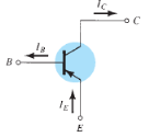
Fig. 9 : PNP common emitter (Ref. 2)
Now, to study the behaviour of the device we require two characteristics:
Input Characteristic Curve
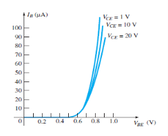
Fig.10: Input Characteristic Curve (Ref. 2)
It is the graph between the input current IB to the input voltage VBE for a range of values of output voltage VCE.
Note that the magnitude IB of is in micro amperes and that of IC is in milli amperes.
Output Characteristic Curve
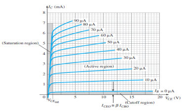
Fig.11: Output Characteristic Curve (Ref. 2)
It is the graph between the output current IC to the output voltage VCE for a range of values of input current IB.
It has three basic regions:
Active Region
- Here, the base-emitter junction is forward biased and collector base junction is reverse biased.
- These are the same conditions that existed in the active region of the common base configuration.
- This can be employed for voltage, current or power amplification.
Cut-off Region
- Here IC is not equal to zero when IB is zero.
- For linear amplification purposes, it is defined as IC = ICEO .
- The region below IB = 0µA is to be avoided for undistorted output signal.
- When the transistor is used as a switch, the condition should be ideally IC = 0mA for a chosen VCE voltage.
Saturation Region
- It is the region that lies towards the left of VCE = 0V.
Common Collector Configuration
The notation and symbols of npn and pnp transistors are given below:
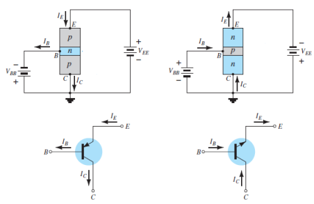
Fig. 12: NPN CC and PNP CC (Ref. 2)
In the above figure all the currents are shown in their actual conventional directions.
It is used for impedence matching purposes as it has high input impedence and low output impedence.
It can be designed using common emitter characteristics.
The output characteristics of common collector is same as that of common emitter configuration for all practical purposes.
The output characteristics are a plot between IE versus VCE for all values of IB.
The input current of common collector is same as that of common emitter configuration.
Here the region of operation will ensure that maximum ratings are not being exceeded and output ratings have minimum distortion.
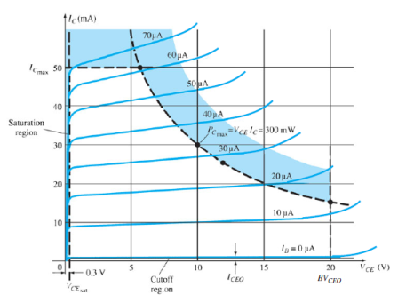
Fig.13: Output Characteristic Curve (Ref. 2)
The characteristics specifying the minimum VCE that can be applied without entering the non-linear region is saturation region.
The maximum power dissipation is given by,
P = VCE . IC
The hybrid two port model is shown below.
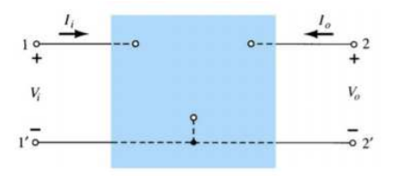
Vi = h11Ii + h12Vo
Io = h21Ii + h22Vo
h11 = hi = Vi/Io for Vo =0 [Input resistance]
h12 = hr = Vi/Vo for Ii =0 [Reverse voltage gain]
h21 = hf = Io/Ii for Vo =0 [forward current gain]
h22 = ho = Io/Vo for Ii =0 [output admittance]
The hybrid equivalent model is shown below

The transistor model has three terminals with two ports.
hi = input resistance
ho= output conductance
hr= Vi/Vo = reverse transfer voltage
hf= Io/Ii = forward transfer current ratio
The simplified model is shown below
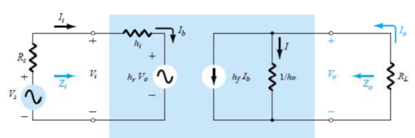
Finding current gain Ai
Applying KCL at the output of above circuit
Io =I + hf Ib = Vo ho + hf Ib
Vo = -Io RL
Io =-Io RL ho + hf Ib
Io (1 + RL ho) = hf Ib
Ai = Io/Ib = hf/(1 + RL ho)
Finding Voltage Gain AV
Applying KVL at input of the above h-model
Vi = hi Ib + hr Vo
But Ib = (1 + ho RL)/hf
Io = - Vo/RL
Substituting in above equation and solving for Vo/Vi we get
Av = -hfRL/hi + (hi ho- hf hr) RL
Finding Input Impedance Zi
Vi = hi Ib + hr Vo
Io = - Vo/RL
Ai = Io/Ib
Vi = hi Ib- hrRLAiIb
Zi = Vi/Ib = hi - hrRLAi
Finding Output impedance Zo
It is ratio of output voltage to output current with Vs =0
Io = Voho + hfIb
Ii = -hrVo/Rs + hi
Zo = Vo/Io = 1/[ho – (hfhr/hi+ Rs)]
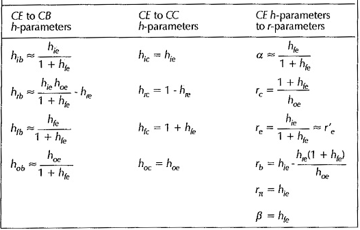
Table of hybrid parameters for CE, CB and CC
FET-Operation
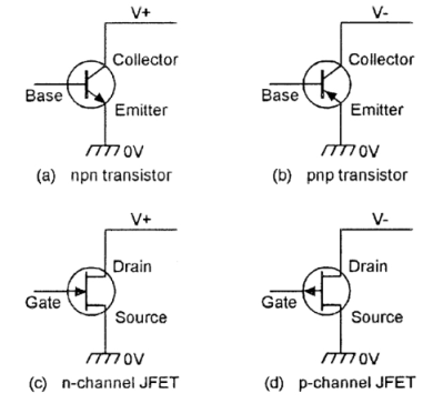
- An FET is a three-terminal amplifying device.
- Its terminals are source, gate, and drain, which acts respectively like emitter, base, and collector of a normal transistor.
- There are two distinct families of FETs.
- The first is known as ‘junction-gate’ types of FETs or JUGFET or JFET.
- The second family is called ‘insulated-gate’ FETs or Metal Oxide Semiconductor FETs or MOSFET.
- ‘N-channel’ and ‘p-channel’ are the two versions of both types of FET.
Operation
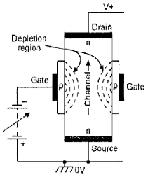
- N-channel FET consists of n-type semiconductor material with a drain terminal and a source terminal at opposite ends.
- A p-type gate is joined in the middle section of the n-type bar, thus forming a p-n junction.
- The drain terminal is connected to a positive supply and the gate is biased at a value that is negative (or equal) to the source voltage, thus reverse-biasing the JFET’s internal p-n junction, and accounting for its very high input impedance.
- When gate = 0V, a current flow from drain to source via a conductive ‘channel’ and the n-type bar is formed.
- When gate = negative , a high resistance region is formed within the junction, thus reduces the magnitude of the drain-to-source current and width of the n-type conduction channel.
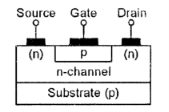
- Thus, the basic JFET passes maximum current when its gate bias is zero, and its current is reduced or ‘depleted’ when the gate bias is increased. It is thus known as a ‘depletion-type’ n-channel JFET.
I-V characteristics
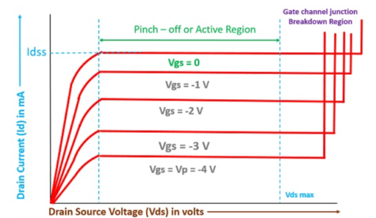
Output Characteristics or Drain Characteristics
- In the absence of external bias: In this case, as there is no voltage between gate and source terminal, thus, the drain current will flow from drain terminal to source terminal. We have already discussed in the working of JFET that majority charge carriers flow from source to drain and as a consequence of which the current flows from drain to source.
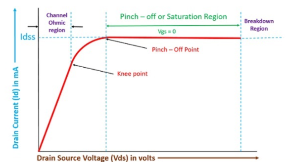
2. With external bias: When the external bias is applied to the gate-source terminal, the gate-source terminal becomes reversed bias externally. Obviously, if we are supplying an external voltage, then we can achieve the pinch-off point quite early as compared to the circuit which is not biased.
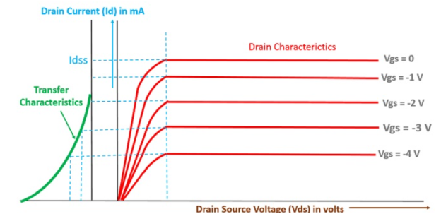
Transfer Characteristics
The transfer characteristics can be determined by observing different values of drain current with variation in gate-source voltage provided that the drain-source voltage should be constant. The transfer characteristics are just opposite to drain characteristics.
MOSFETs- types, Operations and their Characteristics
The MOSFET (Metal Oxide Semiconductor Field Effect Transistor) transistor is a semiconductor device which is widely used for switching and amplifying electronic signals in the electronic devices.
It is a core of integrated circuit and is designed and fabricated in a single chip because of its small size.
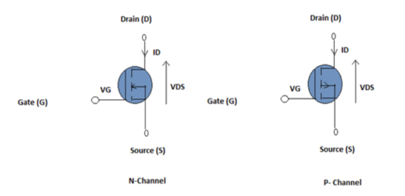
It is a four terminal device with source(S), gate (G), drain (D) and body (B) terminals.
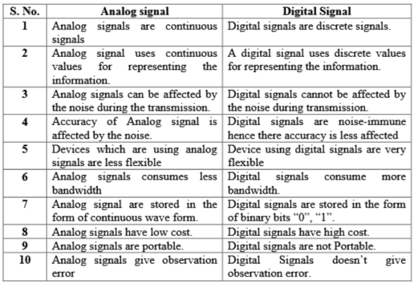
The body of the MOSFET is connected to the source hence making it a three terminal device like field effect transistor. It can be used in both analog and digital circuits.
Operation
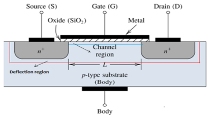
The MOSFET works by electronically varying the width of a channel along which charge carriers flow (electrons or holes).
The charge carriers enter the channel through source and exit via the drain.
The width of the channel is controlled by the gate voltage which is located between source and drain.
It is insulated from the channel near an extremely thin layer of metal oxide.
Function:
- Depletion Mode
When there is no voltage on the gate, the channel shows maximum conductance. When the voltage on the gate is either positive or negative, the channel conductivity decreases.
2. Enhancement Mode
The device does not conduct when there is no voltage on the gate. As the voltage increases on the gate, the better the device can conduct.
Working:
The aim of the MOSFET is to be able to control the voltage and current flow between the source and drain. It works like a switch.
The working depends upon the MOS capacitor.
The MOS capacitor is the main part of MOSFET.
The semiconductor surface at the below oxide layer is located between source and drain terminal. It can be inverted from p-type to n-type by applying positive or negative gate voltages respectively.
When the positive gate voltage is applied, the holes present under the oxide layer repel with a repulsive force and holes are pushed downward with the substrate.
The depletion region populated by the negative charges is the acceptor atoms. The positive voltage also attracts electrons. Now, if a voltage is applied between the drain and source, the current flows between the source and drain and the gate voltage controls the electrons in the channel.
Characteristics:
MOSFET is seen to exhibit three operating regions viz.,
- Cut-Off Region
Cut-off region is a region in which the MOSFET will be OFF as there will be no current flow through it. In this region, MOSFET behaves like an open switch and is thus used when they are required to function as electronic switches. - Ohmic or Linear Region
Ohmic or linear region is a region where in the current IDS increases with an increase in the value of VDS. When MOSFETs are made to operate in this region, they can be used as amplifiers. - Saturation Region
In saturation region, the MOSFETs have their IDS constant inspite of an increase in VDS and occurs once VDS exceeds the value of pinch-off voltage VP. Under this condition, the device will act like a closed switch through which a saturated value of IDS flows. As a result, this operating region is chosen whenever MOSFETs are required to perform switching operations.
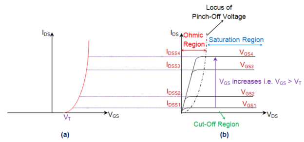
Fig: (a) Transfer Characteristics (b) Output Characteristics of NMOS
Introduction to number system and conversions
A digital system understands positional number system where there are few symbols called digits and these symbol represents different values depending on their position in the number.
A value of the digit is determined by using
- The digit
- Its position
- The base of the number system
Decimal Number System
- Its the system that we use in our daily life. It has a base 10 and uses 10 digits from 0 to 9.
- Here, the successive positions towards the left of the decimal point represent units, tens, hundreds, thousands and so on.
- Each and every position represents a specific power of the base (10). For example, the decimal number 4321 consists of the digit 1 in the units position, 2 in the tens position, 3 in the hundreds position, and 4 in the thousands position, and its value can be written as
(1×1000) + (2×100) + (3×10) + (4×l)
(1×10³) + (2×10²) + (3×101) + (4×l00)
1000 + 200 + 30 + 1
1234
- As a computer programmer, we should understand the following number systems used in computers.
S.N. | Number System & Description |
1 | Binary Number System Base 2. Digits used: 0 and 1 |
2 | Octal Number System Base 8. Digits used: 0 to 7 |
3 | Hexa Decimal Number System Base 16. Digits used: 0 to 9, Letters used: A- F |
Binary their conversion
- It uses two digits 0 and 1.
- It is also called as base 2 number system.
- Here, each position in any binary number represents a power of the base (2). Example: 23
- The last position represents a y power of the base (2). Example: 2y where y represents the last position.
Example
Binary Number: 101112
Calculating the Decimal Equivalent of binary number −
Step | Binary Number | Decimal Number |
Step 1 | 101012 | ((1 × 24) + (0 × 23) + (1 × 22) + (1 × 21) + (1 × 20))10 |
Step 2 | 101012 | (16 + 0 + 4 + 2 + 1)10 |
Step 3 | 101012 | 2310 |
Note: 101112 is normally written as 10111.
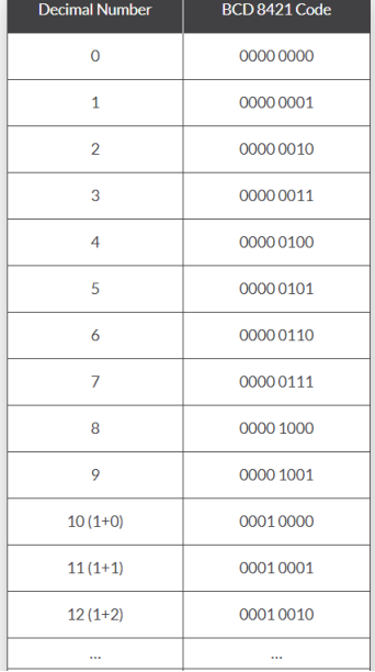
BCD their conversion
BCD numbers are from 0 to 9.
Octal Number System
- It consists of eight digits 0, 1,2,3,4,5,6,7.
- It is also named as base 8 number system.
- Here each position represents a power of the base (8). Example: 82
- The last position represents a y power of the base (8). Example: 8y where y represents the last position .
Example
Octal Number − 125758
Calculating Decimal Equivalent −
Step | Octal Number | Decimal Number |
Step 1 | 125758 | ((1 × 84) + (2 × 83) + (5 × 82) + (7 × 81) + (5 × 80))10 |
Step 2 | 125758 | (4096 + 1024 + 320 + 56 + 5)10 |
Step 3 | 125758 | 550010 |
Note: 125758 is normally written as 12575 in octal.
Hexadecimal Number System
- It uses 10 digits starting from 0,1,2,3,4,5,6,7,8,9 and 6 letters A,B,C,D,E,F.
- These letters represents numbers as A = 10, B = 11, C = 12, D = 13, E = 14, F = 15.
- It is also known as base 16 number system.
- Here each position represents a power of the base (16). Example 161.
- The last position represents a y power of the base (16). Example: 16y where y represents the last position .
Example −
Hexadecimal Number: 19FDA16
Calculating Decimal Equivalent −
Step | Hexadecimal Number | Decimal Number |
Step 1 | 19FDA16 | ((1 × 164) + (9 × 163) + (F × 162) + (D × 161) + (A × 160))10 |
Step 2 | 19FDA16 | ((1 × 164) + (9 × 163) + (15 × 162) + (13 × 161) + (10 × 160))10 |
Step 3 | 19FDA16 | (65536 + 36864 + 3840 + 208 + 10)10 |
Step 4 | 19FDA16 | 10645810 |
Note − 19FDA16 is normally written as 19FDA in hexa decimal.
Decimal to Any Base System
It includes the following steps:
- Firstly, divide the decimal number which is to be converted by the value of its new base.
- Then, after getting the remainder from the above step make it the rightmost digit (least significant digit) i.e. LSD of new base number.
- Further divide the quotient by the new base.
- Then record the remainder from the above step as the next digit (towards the left) of the new base number.
- Repeat these steps and get remainders from right to left till the quotient becomes zero.
- The last remainder obtained will be the Most Significant Digit (MSD) of the new base number.
For example −
Decimal Number: 2710
Calculating Binary Equivalent −
Step | Operation | Result | Remainder |
Step 1 | 27 / 2 | 13 | 1 |
Step 2 | 13 / 2 | 6 | 1 |
Step 3 | 6 / 2 | 3 | 0 |
Step 4 | 3 / 2 | 1 | 1 |
Step 5 | 1 / 2 | 0 | 1 |
Hence, the remainders are arranged in the reverse order and we get:
Decimal Number − 2710 = Binary Number − 110112.
Conversions
There are many techniques which are used to convert numbers from one base to another. These are as follows −
- Decimal to any other Base System
- Any Base System to Decimal
- Any Base System to Non-Decimal
- Binary to Octal
- Octal to Binary
- Binary to Hexadecimal
- Hexadecimal to Binary
Any Base System to Decimal System
- Here, the column (positional) value of each digit (this depends on the position of the digit and the base of the number system) is multiplied with the obtained column values of the digits in the corresponding columns.
- The sum the products are then calculated which gives the total equivalent value in decimal.
For example:
Binary Number − 111102
Calculating Decimal Equivalent −
Step | Binary Number | Decimal Number |
Step 1 | 111102 | ((1 × 24) + (1 × 23) + (1 × 22) + (1 × 21) + (0 × 20))10 |
Step 2 | 111102 | (16 + 8 + 4 + 2 + 0)10 |
Step 3 | 111102 | 3010 |
Binary Number − 111102 = Decimal Number − 3010
Any Base System to Non-Decimal System
- The original number is converted to its equivalent decimal number (base 10).
- Then the decimal number so obtained is further converted to the new base number.
Example
Octal Number − 268
Calculating its Binary Equivalent −
Step 1 – Converting octal to Decimal
Step | Octal Number | Decimal Number |
Step 1 | 268 | ((2 × 81) + (6 × 80))10 |
Step 2 | 268 | (16 + 6 )10 |
Step 3 | 268 | 2210 |
Octal Number − 268 = Decimal Number − 2210
Step 2 − Converting Decimal to Binary
Step | Operation | Result | Remainder |
Step 1 | 22 / 2 | 11 | 0 |
Step 2 | 11 / 2 | 5 | 1 |
Step 3 | 5 / 2 | 2 | 1 |
Step 4 | 2 / 2 | 1 | 0 |
Step 5 | 1 / 2 | 0 | 1 |
Decimal Number − 2210 = Binary Number − 101102
Octal Number − 268 = Binary Number − 101102
Binary to Octal
- Dividing the binary digits into groups of three starting from right to left.
- Converting each group of three binary digits into one octal digit.
For example:
Binary Number − 101012
Its Octal Equivalent −
Step | Binary Number | Octal Number |
Step 1 | 101012 | 010 101 |
Step 2 | 101012 | 28 58 |
Step 3 | 101012 | 258 |
Binary Number − 101012 = Octal Number − 258
Octal to Binary
- Converting each octal digit to a 3 digit binary number and they can be treated as decimal number for this conversion.
- Then combining all the resulting binary groups into a single binary number.
For example:
Octal Number − 258
Its Binary Equivalent −
Step | Octal Number | Binary Number |
Step 1 | 258 | 210 510 |
Step 2 | 258 | 0102 1012 |
Step 3 | 258 | 0101012 |
Octal Number − 258 = Binary Number − 101012
Binary to Hexadecimal
- Dividing the binary digits into groups of four (starting from right to left).
- Then converting each group of four binary digits into one hexadecimal number.
For example:
Binary Number − 101012
Its hexadecimal Equivalent −
Step | Binary Number | Hexadecimal Number |
Step 1 | 101012 | 0001 0101 |
Step 2 | 101012 | 110 510 |
Step 3 | 101012 | 1516 |
Binary Number − 101012 = Hexadecimal Number − 1516
Hexadecimal to Binary
- Converting each hexadecimal digit to a 4 digit binary number and they can be treated as decimal number.
- Combining all the resulting binary groups into a single binary number.
For example:
Hexadecimal Number − 1516
Its Binary Equivalent −
Step | Hexadecimal Number | Binary Number |
Step 1 | 1516 | 110 510 |
Step 2 | 1516 | 00012 01012 |
Step 3 | 1516 | 000101012 |
Hexadecimal Number − 1516 = Binary Number − 101012
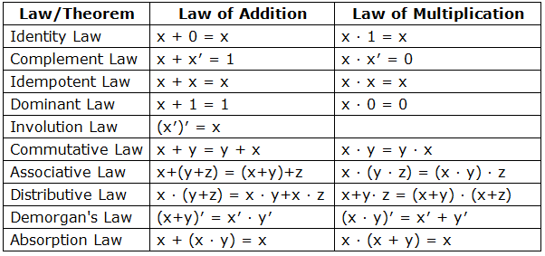
Demorgan theorems
- It is useful in finding the complement of Boolean function.
- It states that “The complement of logical OR of at least two Boolean variables is equal to the logical AND of each complemented variable”.
- It can be represented using 2 Boolean variables x and y as
(x + y)’ = x’.y’
- The dual of the above Boolean function is
(x.y)’ = x’ + y’
- Therefore, the complement of logical AND of the two Boolean variables is equivalent to the logical OR of each complemented variable.
- Similarly, DeMorgan’s theorem can be applied for more than 2 Boolean variables also.
Simplification of Boolean Functions
Numerical
- Simplify the Boolean function,
f = p’qr + pq’r + pqr’ + pqr
Method 1
Given
f = p’qr + pq’r + pqr’ +pqr.
In first and second term r is common and in third and fourth terms pq is common.
So, taking out the common terms by using Distributive law we get,
⇒ f = (p’q + pq’)r + pq(r’ + r)
The terms present in first parenthesis can be simplified by using Ex-OR operation.
The terms present in second parenthesis is equal to ‘1’ using Boolean postulate we get
⇒ f = (p ⊕q)r + pq(1)
The first term can’t be simplified further.
But, the second term is equal to pq using Boolean postulate.
⇒ f = (p ⊕q)r + pq
Therefore, the simplified Boolean function is f = (p⊕q)r + pq
Method 2
Given f = p’qr + pq’r + pqr’ + pqr.
Using the Boolean postulate, x + x = x.
Hence we can write the last term pqr two more times.
⇒ f = p’qr + pq’r + pqr’ + pqr + pqr + pqr
Now using the Distributive law for 1st and 4th terms, 2nd and 5th terms, 3rdand 6th terms we get.
⇒ f = qr(p’ + p) + pr(q’ + q) + pq(r’ + r)
Using Boolean postulate, x + x’ = 1 and x.1 = x for further simplification.
⇒ f = qr(1) + pr(1) + pq(1)
⇒ f = qr + pr + pq
⇒ f = pq + qr + pr
Therefore, the simplified Boolean function is f = pq + qr + pr.
Hence we got two different Boolean functions after simplification of the given Boolean function. Functionally, these two functions are same. As per requirement, we can choose one of them.
Numerical
Find the complement of the Boolean function,
f = p’q + pq’.
Solution:
Using DeMorgan’s theorem, (x + y)’ = x’.y’ we get
⇒ f’ = (p’q)’.(pq’)’
Then by second law, (x.y)’ = x’ + y’ we get
⇒ f’ = {(p’)’ + q’}.{p’ + (q’)’}
Then by using, (x’)’=x we get
⇒ f’ = {p + q’}.{p’ + q}
⇒ f’ = pp’ + pq + p’q’ + qq’
Using x.x’=0 we get
⇒ f = 0 + pq + p’q’ + 0
⇒ f = pq + p’q’
Therefore, the complement of Boolean function, p’q + pq’ is pq + p’q’.
The basic gates are namely AND gate, OR gate & NOT gate.
AND gate
It is a digital circuit that consists of two or more inputs and a single output which is the logical AND of all those inputs. It is represented with the symbol ‘.’.
The following is the truth table of 2-input AND gate.
A | B | Y = A.B |
0 | 0 | 0 |
0 | 1 | 0 |
1 | 0 | 0 |
1 | 1 | 1 |
Here A, B are the inputs and Y is the output of two input AND gate.
If both inputs are ‘1’, then only the output, Y is ‘1’. For remaining combinations of inputs, the output, Y is ‘0’.
The figure below shows the symbol of an AND gate, which is having two inputs A, B and one output, Y.

Fig. : AND gate (ref. 1)
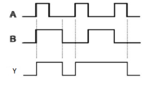
Timing Diagram:

OR gate
It is a digital circuit which has two or more inputs and a single output which is the logical OR of all those inputs. It is represented with the symbol ‘+’.
The truth table of 2-input OR gate is:
A | B | Y = A + B |
0 | 0 | 0 |
0 | 1 | 1 |
1 | 0 | 1 |
1 | 1 | 1 |
Here A, B are the inputs and Y is the output of two input OR gate.
When both inputs are ‘0’, then only the output, Y is ‘0’. For remaining combinations of inputs, the output, Y is ‘1’.
The figure below shows the symbol of an OR gate, which is having two inputs A, B and one output, Y.

Fig. : OR gate (ref. 1)
Timing Diagram:
NOT gate
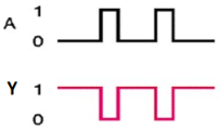
It is a digital circuit that has one input and one output. Here the output is the logical inversion of input. Hence, it is also called as an inverter.
The truth table of NOT gate is:
A | Y = A’ |
0 | 1 |
1 | 0 |
Here A and Y are the corresponding input and output of NOT gate. When A is ‘0’, then, Y is ‘1’. Similarly, when, A is ‘1’, then, Y is ‘0’.
The figure below shows the symbol of NOT gate, which has one input, A and one output, Y.

Fig. : NOT gate (ref. 1)
Timing Diagram:
Universal gates
NAND & NOR gates are known as universal gates.
We can implement any Boolean function by using NAND gates and NOR gates alone.
NAND gate
It is a digital circuit which has two or more inputs and single output and it is the inversion of logical AND gate.
The truth table of 2-input NAND gate is:
A | B | Y = (A.B)’ |
0 | 0 | 1 |
0 | 1 | 1 |
1 | 0 | 1 |
1 | 1 | 0 |
Here A, B are the inputs and Y is the output of two input NAND gate. When both inputs are ‘1’, then the output, Y is ‘0’. If at least one of the input is zero, then the output, Y is ‘1’. This is just the inverse of AND operation.
The image shows the symbol of NAND gate:

Fig.: NAND gate (ref. 1)
NAND gate works same as AND gate followed by an inverter.
Timing Diagram:
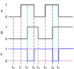
NOR gate
It is a digital circuit that has two or more inputs and a single output which is the inversion of logical OR of all inputs.
The truth table of 2-input NOR gate is:
A | B | Y = (A+B)’ |
0 | 0 | 1 |
0 | 1 | 0 |
1 | 0 | 0 |
1 | 1 | 0 |
Here A and B are the two inputs and Y is the output. If both inputs are ‘0’, then the output is ‘1’. If any one of the input is ‘1’, then the output is ‘0’. This is exactly opposite to two input OR gate operation.
The symbol of NOR gate is:

Fig.: NOR gate (ref. 1)
NOR gate works exactly same as that of OR gate followed by an inverter.
Timing Diagram:
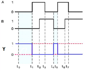
Special Gates
Ex-OR gate
It stands for Exclusive-OR gate. Its function varies when the inputs have even number of ones.
The truth table of 2-input Ex-OR gate is:
A | B | Y = A⊕B |
0 | 0 | 0 |
0 | 1 | 1 |
1 | 0 | 1 |
1 | 1 | 0 |
Here A, B are the inputs and Y is the output of two input Ex-OR gate. The output (Y) is zero instead of one when both the inputs are one.
Therefore, the output of Ex-OR gate is ‘1’, when only one of the two inputs is ‘1’. And it is zero, when both inputs are same.
The symbol of Ex-OR gate is as follows:

Fig.: XOR gate (ref. 1)
It is similar to that of OR gate with an exception for few combination(s) of inputs. Hence, the output is also known as an odd function.
Timing Diagram:
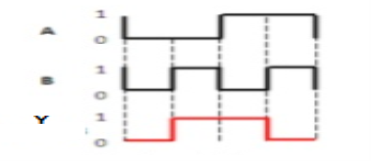
Ex-NOR gate
It stands for Exclusive-NOR gate. Its function is same as that of NOR gate except when the inputs having even number of ones.
The truth table of 2-input Ex-NOR gate is:
A | B | Y = A⊙B |
0 | 0 | 1 |
0 | 1 | 0 |
1 | 0 | 0 |
1 | 1 | 1 |
Here A, B are the inputs and Y is the output. It is same as Ex-NOR gate with the only modification in the fourth row. The output is 1 instead of 0, when both the inputs are one.
Hence the output of Ex-NOR gate is ‘1’, when both inputs are same and 0, when both the inputs are different.
The symbol of Ex-NOR gate is:

Fig.: XNOR gate (ref. 1)
It is similar to NOR gate except for few combination(s) of inputs. Here the output is ‘1’, when even number of 1 is present at the inputs. Hence is also called as an even function.
Timing Diagram:
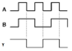
It is the most suitable method for minimizing Boolean functions of 2 variables to 5 variables.
2 Variable K-Map
It has 4 number of cells since the number of variables is two.
The 2 variable K-Map is :

Fig.6 : 2 variable K-Map (ref. 1)
- The only way to group4 adjacent min terms.
- The possible combinations are {(m0, m1), (m2, m3), (m0, m2) and (m1, m3)}.
3 Variable K-Map
It has 8 number of cells since the number of variables is 3.
The 3 variable K-Map is:
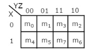
Fig.7 : 3 variable K-Map
- The only way to group 8 adjacent min terms.
- The possible are {(m0, m1, m3, m2), (m4, m5, m7, m6), (m0, m1, m4, m5), (m1, m3, m5, m7), (m3, m2, m7, m6) and (m2, m0, m6, m4)}.
- The possible combinations of grouping 2 adjacent min terms are {(m0, m1), (m1, m3), (m3, m2), (m2, m0), (m4, m5), (m5, m7), (m7, m6), (m6, m4), (m0, m4), (m1, m5), (m3, m7) and (m2, m6)}.
- If x=0, then 3 variable K-map becomes 2 variable K-map.
4 Variable K-Map
It has 16 number of cells since the number of variables is 4.
The 4 variable K-Map is:

Fig.8 : 4 variable K-Map
- The only way to group 8 adjacent min terms.
- Let R1, R2, R3 and R4 represents the min terms of first row, second row, third row and fourth row respectively.
- Similarly, C1, C2, C3 and C4represents the min terms of first column, second column, third column and fourth column respectively.
- The possible combinations are {(R1, R2), (R2, R3), (R3, R4), (R4, R1), (C1, C2), (C2, C3), (C3, C4), (C4, C1)}.
- If w=0, then 4 variable K-map becomes 3 variable K-map.
Rules for simplifying K-maps:
- Selecting K-map on the basis of number of variables present in the Boolean function.
- If the Boolean function is in Max terms form, then place the zeroes at respective Max term cells in the K-map.
- If the Boolean function is in PoS form, then place the zeroes wherever required in K-map for which the given sum terms are valid.
- The maximum possibilities of grouping are checked for adjacent zeroes.
- It should be of powers of two.
- Starting from highest power of two and to the least power of two.
- Highest power is equivalent to the number of variables considered in K-map and least power is zero.
- Each group will give either a literal or one sum term.
- It is known as prime implicant.
- The prime implicant is an essential prime implicant when at least a single ‘0’ is not covered with any other groups but only that grouping covers.
- The simplified Boolean function contains all essential prime implicants and only the required prime implicants.
Numericals
Simplify f(X,Y,Z)=∏M(0,1,2,4)f(X,Y,Z)=∏M(0,1,2,4)using K-map.

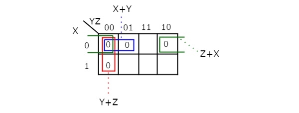
Therefore, the simplified Boolean function is
f = (X + Y).(Y + Z).(Z + X)
Simplify:
F(P,Q,R,S)=∑(0,2,5,7,8,10,13,15)
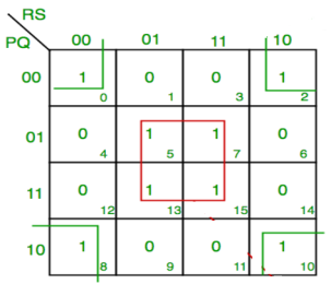
F = P’Q’R’S’ + PQ’R’S’ + P’Q’RS’ +PQ’RS’ + QS
F = P’Q’S’ + PQ’S’ + QS
F = Q’S’ +QS
Simplify:
F(A,B,C)=π(0,3,6,7)
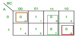
F = A’BC +ABC +A’B’C’ +ABC’
F = BC + C’ ( A’B’ + AB )
4. Quine-McCluskey Tabular Method
- K-map method is a convenient method for minimization of Boolean functions up to 5 variables. But, it is very difficult to simplify more than 5 variables by using this method.
- Quine-McClukey is a tabular method based on the concept of prime implicants.
- Prime implicant is a product (or sum) term, which cannot be further reduced by combining with any other product (or sum) terms in the given Boolean function.
- This tabular method gets the prime implicants by repeatedly using the following Boolean identity.
Xy + xy’ = x(y + y’) = x.1 = x
Procedure of Quine-McCluskey Tabular Method
Steps for simplifying Boolean functions using Quine-McCluskey method:
Step 1 − Arranging the given min terms in ascending order and making groups based on the number of one’s present in the binary representations.
So, there are at most ‘n+1’ groups if there are ‘n’ Boolean variables or ‘n’ bits in the binary equivalent of min terms.
Step 2 − Comparing the min terms present in successive groups. If there is a change in only one-bit position, then taking the pair of two min terms. Placing the symbol ‘_’ in the differed bit position and keeping the remaining bits as it is.
Step 3 − Repeating step2 with newly formed terms till we get all required prime implicants.
Step 4 − Formulating the prime implicant tablewhich consists of set of rows and columns. It can be placed row wise and min terms can be placed column wise. Put ‘1’ in the cells corresponding to the min terms that are covered in each prime implicant.
Step 5 – Nowfinding the essential prime implicants by observing each column. If the min term is covered by one prime implicant, then it is called as essential prime implicant. They will be a part of the simplified Boolean function.
Step 6 –The prime implicant table is reduced by removing the row and columns of each essential prime implicant corresponding to the min terms .This process is stopped when all min terms of given Boolean function are over.
Example
Simplify, f(W,X,Y,Z)=∑m(2,6,8,9,10,11,14,15) and f(W,X,Y,Z)=∑m(2,6,8,9,10,11,14,15)
UsingQuine-McClukey tabular method.
Solution:
Group Name | Min terms | W | X | Y | Z |
GA1 | 2 | 0 | 0 | 1 | 0 |
8 | 1 | 0 | 0 | 0 | |
GA2 | 6 | 0 | 1 | 1 | 0 |
9 | 1 | 0 | 0 | 1 | |
10 | 1 | 0 | 1 | 0 | |
GA3 | 11 | 1 | 0 | 1 | 1 |
14 | 1 | 1 | 1 | 0 | |
GA4 | 15 | 1 | 1 | 1 | 1 |
Group Name | Min terms | W | X | Y | Z |
GB1 | 2,6 | 0 | - | 1 | 0 |
2,10 | - | 0 | 1 | 0 | |
8,9 | 1 | 0 | 0 | - | |
8,10 | 1 | 0 | - | 0 | |
GB2 | 6,14 | - | 1 | 1 | 0 |
9,11 | 1 | 0 | - | 1 | |
10,11 | 1 | 0 | 1 | - | |
10,14 | 1 | - | 1 | 0 | |
GB3 | 11,15 | 1 | - | 1 | 1 |
14,15 | 1 | 1 | 1 | - | |
|
|
|
|
|
|
Group Name | Min terms | W | X | Y | Z |
GB1 | 2,6,10,14 | - | - | 1 | 0 |
2,10,6,14 | - | - | 1 | 0 | |
8,9,10,11 | 1 | 0 | - | - | |
8,10,9,11 | 1 | 0 | - | - | |
GB2 | 10,11,14,15 | 1 | - | 1 | - |
10,14,11,15 | 1 | - | 1 | - | |
|
|
|
|
|
|
Group Name | Min terms | W | X | Y | Z |
GC1 | 2,6,10,14 | - | - | 1 | 0 |
| 8,9,10,11 | 1 | 0 | - | - |
GC2 | 10,11,14,15 | 1 | - | 1 | - |
Therefore, the prime implicants are YZ’, WX’ & WY.
The prime implicant table is shown below.
Min terms / Prime Implicants | 2 | 6 | 8 | 9 | 10 | 11 | 14 | 15 |
YZ’ | 1 | 1 |
|
| 1 |
| 1 |
|
WX’ |
|
| 1 | 1 | 1 | 1 |
|
|
WY |
|
|
|
| 1 | 1 | 1 | 1 |
The reduced prime implicant table is shown below.
Min terms / Prime Implicants | 8 | 9 | 11 | 15 |
WX’ | 1 | 1 | 1 |
|
WY |
|
| 1 | 1 |
Min terms / Prime Implicants | 15 |
WY | 1 |
Hence, f(W,X,Y,Z) = YZ’ + WX’ + WY.
Simplify ( ref : internet)
Y(A,B,C,D) =∑ m(0,1,3,7,8,9,11,15)
Groups are made with respect to the no. Of one’s present.
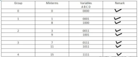
Now, comparing with the above table wherever we have a different bit present we put a ’-‘ there.

The same thing is done by comparing from the above table.

The table for prime implicants is:

Rounding the min terms which has X in column and hence the final answer is B’C’ + CD.
References
- S. Salivahanan, N. Suresh Kr. & A. Vallavaraj, ―Electronic Devices & Circuit‖, Tata McGraw Hill,
2008
2. Millman, Halkias and Jit, ―Electronic devices and circuits‖ McGraw Hill
3. Boylestad & Nashelsky, ―Electronic Devices & Circuits‖, Pearson Education, 10TH Edition.
4. Sedra & Smith, ―Micro Electronic Circuits‖ Oxford University Press, VI Edition
5. Robert T. Paynter, ―Introducing Electronic Devices & Circuits‖, Pearson Education, VII Edition, 2006