UNIT 1
Semiconductor Physics
N type Semiconductor:-
To increase the number of conduction band electrons intrinsic silicon , pentavalent imparity atoms are added. These are atoms with five valence electrons such as
i) arsenic (as)
Ii) phosphors (p)
Iii) Bismuth (Bi)
Iii) Antimony ( sb)
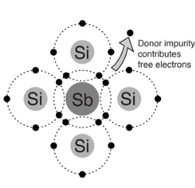
- Pentavalent impurity atom in a silicon crystal. An antimony (sb) impurity atom shown above-
- Each pentavalent atom forms covalent bonds with four adjustment silicon atoms, leaving one extra electron.
- The pentavalent atom gives up on electron, it often called a donor atom.
- Majority and minority carriers: - A type here means negative charge of an electron. Electron is called the majority carriers in n-type material.
- Hole in an n-type material are called minority carriers
P Type Semiconductor :-
To increase the number of holes in intrinsic silicon trivalent impurity atoms are added these are atoms with their valence electrons such as
i) Baron(B)
Ii) Indium(IN)
Iii)Gallium(GO)
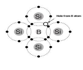
- Trivalent impurity atom in a silicon crystal structure . A) boron (B) impurity atom is shown in the center.
- The number of holes can be carefully controlled by the number of trivalent impurity atoms added to the silicon .
- A Hole created by the doping process is not accompanied by a conduction (free) electron.
- Trivalent Atom can take an electron it is often referred to as on accepted atom
V Barrier
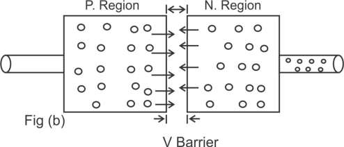
- A Forward biased showing the flow of majority carriers and the voltage due to the barrier potential across the depletion region-
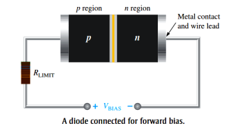
- To bias a diode apply d,cvtg across it .
- Forward bias is the condition that allows current through the PN junction.
- Negative side of VBIAS is connected to the N -region of the diode and the positive side is connected to the P- region.
- A selected requirement is that the bias voltage VBIAS must be greater than the barrier potential.
- Because of like charges repel, the negative side of the bias voltage source pushes the free electrons , which are the majority carriers in the N-region towards the PN junction .the flow of free is called Electron Current.
- The –Ve side of the source also provide a continues flow of electrons through the external connection (conductor).
- Into the N-region as show in fig-B
- The bias voltage source imparts sufficient energy to the free electrons for them to overcome the barrier potential of the depletion region and move on through into the 'p' region once in the P-region. These conduction electrons have lost enough energy to immediately combine with holes in the valence band.
- Now the e- are in the valance band in the P-region simply because they have lost too much energy overcoming the barrier potential to remain in the conduction band. Since unlike charge attract, the positive side of the bias voltage source attracts the valence electrons toward the left end of the region.
- The hole in the P-region provide the medium or "Pathway" for these valence electrons to move through the P-region.
- The holes which are the majority carriers in the P-region, effectively (not actually) move to the right toward the junction as shown in fig-B.
- The defective flow of holes is called the hole current.
- As from Fig-B hole current as the flow of valence electrons through the P-region with the holes providing the only means for these electrons to flow.
- As the electrons flow out of the P-region through the external connection and to the positive side of the bias in the P-region at the same time these electrons become conduction electrons in the mater conductor.
- To these is a continues availability of holes effectively moving towards the PN junction stream of electrons as they come across the junction in to the P-region.
The effect of forward bias on the depletion region:-
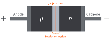


+ -


 -
-
Depletion Region
- Forward bias narrows the depletion region & produce a vtg drop across pn junction equal to the barrier potential.
- As more electrons flow into the depletion region , the number of positive ions is reduce . As more notes effectively flow into the depletion region on the other side of the pn junction ,the number of -ve ions is reduce this reduction in positive & -ve ions during forward bias causes the depletion region to narrow.
The Effect of the Barrier Potential during forward bias:-
- The electronic field between the positive and negative ions in the depletion region on either side of the junction creates an energy bill, that prevent free R form diffusing across the junction at equilibrium this is known as the barrier potential
- When forward bias is applied the free electrons are provided with enough energy from the bias voltage source to overcome the barrier potential and effectively climb the energy bill and cross the depletion region.
- The energy that the electronics repair in order to pass through the depletion region is equal to the barrier potential.
- Electron gives up an amount of energy equivalent to the barrier potential when they cross the depletion region.
- This energy loss results in a vtg drop across the pn junction equals to the barrier potential (0.7v)
- An additional small vtg drop across the P & N regions due to the internal resistance of the material.
- For doped Semiconductor material, this resistance called the dynamic resistance is very small and can usually be neglected.
REVERSE BIAS:-
Reverse bias is the condition the essentially prevents current through the diode.


P-region N- region


- +
V BIAS
A Diode connected for Reverse Biased-
- Because unlike charges attract the positive side of the bia voltage source pulls the free election, which are the majority carriers in the N-region away from the PN junction.
- AS the election flow towards the positive side of the voltage source additional positive ions are created
- This results in a widening of the depletion region and a depletion of majority carriers.


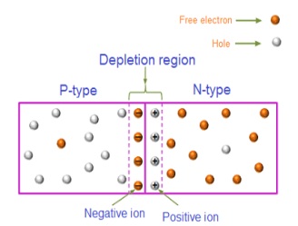
- The diode during the short transition time immediately after reverse bias vtg is applied-
- In the P-region electrons from the negative side of the vtg source enter as valence electron and move from hole to hole toward the depletion region where the creators additional -ve ions.
- This results in a widening of the depletion region and a depletion of majority carriers
- As the depletion region widens the availability of majority carriers decreases
- As more of the N & P regions become depleted of majority carriers, the electric field between the positive and -ve ions increase in strength the depletion region equals the bios vtg .this point the transition current essentially ceases except for a small reverse current that can usually be neglected.
Reverse Current
- Extremely small current that exist in reverse bias after the transition current dies act is caused by the minority carrier in the N& P region that are produced by the manly generated e hole pairs.
- The conduction band in the P-region is at a higher energy level then the conduction band in the N-region. Therefore, the minority easily pass through the depletion region because they required no additional energy.
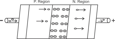
The Extremely small reverse current in a reverse biased diode is due to the minority carriers from thermally generated
e=hole pairs
The Diode - Before doping the p-type & N-type consisting silicon material atom acting as a neutral.
IF a piece of intrinsic silicon is doped so that part is n-type and the other part is p-type, a junction forms at the bounded between the two regions and a diode is created.
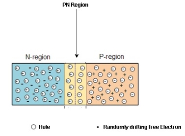
Formation of the Depletion Region
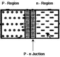
At the instant of junction formation , free electrons in the N-region near the p-n junction being to diffuse across the junction and fall into holes near the junction in the P-region.
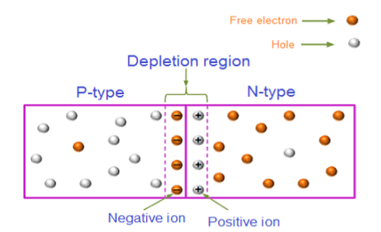
For every electron that defuse across the junction and combines with a hole , a positive charge is left in the region and a ve charge is created in the p-region firming a barriers potential. This action continues until the vtg of the barrier ripples further diffusion.
The Depletion region acts as a barriers to the farther movement of electrons across the junction
As positive ion & -ve ion across the junction produces a electric field across the junction -according to coulombs law.
The potential difference of the electric field across the depletion region is the amount of vtg required to move electronics through the electric field, this potential difference is called the barrier potential & is expressed in volt
The typical barrier potential is approximately 0.7 v for silicon & 0.3 v for germanium at 25c.
V-I characteristics of junction diode
A :- v=A Characteristic for forward bias:-
If (mA)


 C
C

 A B
A B
o 0.7V vf
V-I Characteristics:-
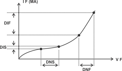
Graph shows how the dynamic resistance decrease as we move up the curve xd= DNF/DIF=
When the forward bias vtg is increased to a value where the vtg across the diode reaches approximately 0.7 v (barrier potential . The forward currant begins to increase rapidly
As we continue to increase the forward bias voltage the current continues to increase very rapidly ,but the voltage across the diode increase only gradually above 0.7 v.
This small increase in the diode vtg above the barrier potential is due to the voltage drop across the internal dynamic resistance of the semi conductive material.
Dynamic resistance:- A Resistance change as move along a V-I curve it is called dynamic or A. C resistance.
 |
B) V- I Characteristics for Reverse biased :-


 VR VBR 0
Knee
When the applied bias voltage is increased to a value where. The reverse vtg across the diode the reaches appropriately 0.7 v (barrier potential) the forward current begins to increase rapidly.
As we continue to increase the bias voltage the current continues to increase very rapidly bit the voltage across the diode increases very little above VBR.
IR increases little above VBR. Resulting in overheating & possible damage.
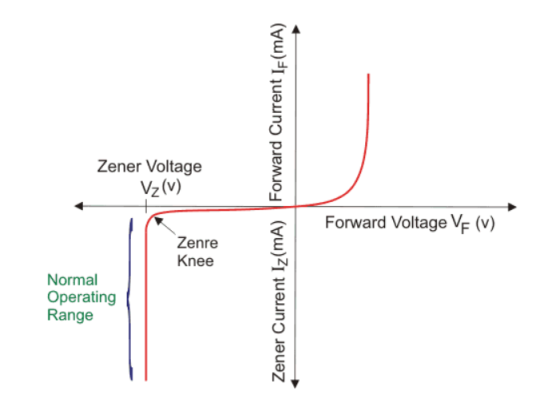
Zener Diode
- Zener diode is a special type of p-n junction semiconductor diode in this diode the reverse breakdown voltage is adjusted precisely between 3v to 200v.
- Its applications are based on this principle hence Zener diode is called as a breakdown diode.
- The doping level of the imparity added to manufacture the zener diode is controlled in order to adjust the precise value of breakdown voltage.
PRINCIPLE OF OPERATION: - A zener diode can be forward biased or reverses biased. Its operation in the forward biased mode is same as that of a p-n junction diode but its operation in the reverse biased mode is sustainably deferent.

Numerical:
A 5.0V stabilized power supply is required to be produced from a 12V DC power supply input source. The maximum power rating PZ of the zener diode is 2W. Using the zener regulator circuit above calculate:
a). The maximum current flowing through the zener diode.
Maximum current = Watts/ Voltage =2W/5V =400mA
b). The minimum value of the series resistor, RS
 = 17.5 Ω
c). The load current IL if a load resistor of 1kΩ is connected across the zener diode.

d). The zener current IZ at full load.
Iz =Is -Il =440mA – 5mA = 395mA
Bridge Rectifier
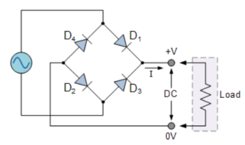
It uses four individual rectifying diodes which are connected in a closed loop called “bridge” configuration to produce the desired output.
It does not require a special centre tapped transformer, hence reducing its size and cost. The single secondary winding is connected one side to the diode bridge network and the other side to the load.
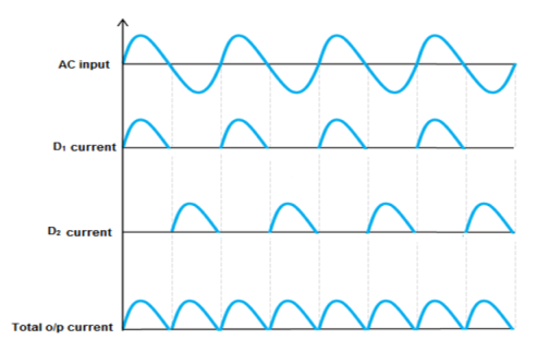
The four diodes D1 to D4 are arranged in “series pairs” and only two diodes conduct current during each half cycle.
During the positive half cycle, diodes D1 and D2 conduct in series while diodes D3 and D4 are reverse biased producing current through the load.
During the negative half cycle, diodes D3 and D4 conduct in series and diodes D1 and D2 are switched “OFF” as they become reverse biased producing current through the load.
During each half cycle the current flows through two diodes instead of just one. The ripple frequency is now twice the supply frequency.
Output Waveform:
Characteristics of full wave rectifier
Ripple factor
The ripple factor is given by

Finally, we get γ = 0.48
Rectifier efficiency
It is defined as the ratio of DC output power to the AC input power.
It can be mathematically written as
η = output PDC / input PAC
The rectifier efficiency of a full wave rectifier is 81.2%.
Peak inverse voltage (PIV)
It is the maximum voltage a diode can withstand in the reverse bias condition.
The peak inverse voltage (PIV) = 2Vsmax
DC output current
The current produced by D1 is Imax / π and the current produced by D2 is Imax / π.
So the output current IDC = 2Imax / π
Where, Imax = maximum DC load current
DC output voltage
The DC output voltage appeared at the load resistor RL is given as
VDC = 2Vmax /π
Where,
Vmax = maximum secondary voltage
Root mean square (RMS) value of load current IRMS
The root mean square (RMS) value of load current in a full wave rectifier is

The root mean square (RMS) value of output load voltage in a full wave rectifier is

Form factor
It is the ratio of RMS value of current to the DC output current
F.F = RMS value of current / DC output current
The form factor of a full wave rectifier is F.F = 1.11
Advantages :
- High rectifier efficiency
- Low power loss
- Low ripples
- It has fewer ripples than the half wave rectifier.
Disadvantages:
- High cost
- The center tapped transformers are expensive and occupy a large space.
Diode Clipper or Limiting Circuits :-
Diode C kts called limiters or clippers are sometimes used to clip off portions of signal voltages above or below certain levels.
Another type of diode ckt called a clamper is used to add or restore a d.c level to an electrical signal.
Below fig a) that limits or clips the positive part of the input voltageAs the ilpvtg goes positive the diode become forward biased Because the cathode is at ground potential (ov)the anode cannot exceed 0.7v (for si)
So point A is limited to 0.7v the diode is reverse biased and appears as an open. The O/P VTG looks like the with a magnitude determined by the voltage divider formed by R1& the load resistor RL.
Vout=(RL/R1+RL) vin
If R1 small compared to RL then vout =vin

Clipper of the positive alternation. The diode is F,B during the +ve alternate RB during –ve alternation:-
Negative Clipper:-

Limiting of the negative alternation the diode is PB during the –ve alternation R.B during the +ve alternation.
During Reverse bias the +ve part of the ilpvtg is clipped off when the diode is forward biased during the –ve part of the ilpvtg is clipped off. When the diode is F.B during the –ve part of the ilpvtg point A is held at 0.7v by the diode is no longer forward biased and a voltage appears across RL proportional to the ilpvtg.
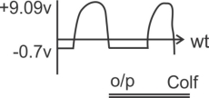
Problem:- What would you expect to see displayed on oscilloscope connected across RL in the Limiter.

The diode is forward biased and conducts when then the i/pvtg goes below -0.7v so for the –ve limiter , the peak o/p vtg across RL can be determined by the following
Equation -
Volt=(RL/R+RL) Vin
=(1k/100+1k)10v
= 1K/1.1K*10
=1*103/1.1*103*10
= 1*104/11*102*10
= 1*104*10-2*10
=10/11 10*10*10/11
Volt=10000/11=9.09V
Biased parallel /Clipper:-1) The level to which an act voltage is limited can be adjusted by adding a bias vtg in series with the diode shown in fig.

The voltage at point A mast equal VBINS+0.7v before the diode will become forward biased & conduct
Once the diode begins to conduct the vtg at point A is limited to VBINS +0.7 so that all ilp above this level is clipped off

To limit a vtg to a specified –ve level the diode & bios vtg must be connected. In this case the vtg at point ‘A’ must go below –VBIN-0.7v to forward biased the diode & initiate limiting action
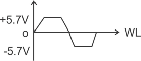
Prob:- fig shows a ckt combing a positive clipper with a-ve clipper .Determine the o/p vtg c/f

When the voltage at point A riches +5.7V diode A conducted and limits the waveform to +5.7v diode D2 does not conduct until the voltage reaches -5.7V
Therefore positive voltages above +5.7V & -vevoltages below -5.7V are clipped off
Diode Clampers:-
1) Positive Clamper:-
Diagram:-

Assumptions :-
1) The V/p is a perfect sine waveform
2)The value of R& C are chosen such that the Line constant T=RC is large equal
3)The diode is an ideal one
4)TheRc time constant is much longer as compared to one cattle period ‘T’ of the input.
RC>100T
Operation :-I n the first negative half cycle after turning on the Ckt the diode acts as a closed S/W & charges the capacitor to peak ilpvtg VM with the polarity shown below

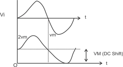
The diode reverse biased in both half cycle so it remains off.
2)Negative Clamper:-

In the first positive half cycle the capacitor will charge through the forward biased to peak vtgvm
The charging takes place very quickly as the diode resistances negligibly small
Once the capacitor charges to vm the diode is reverse biased and stops conducting.

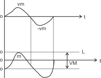
Diagram non ideal diode
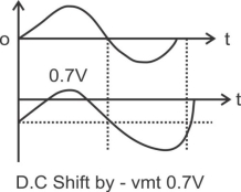
Biased Clamper:-
Diagram:-
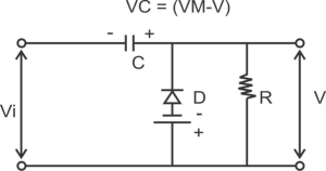
-Clamper with additional dc source:-
Diagram-
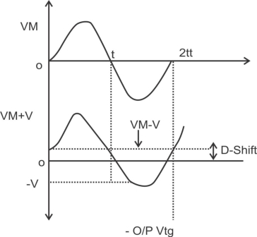
The load vtg W/F shows d.c level shift is positive but less than +vm
Level shift is given by
DG shift=vm-v
Operation:-
In the –ve half cycle ilp the diode will be forward biased and capacitor gets charged to a vtg (vm-v) volts with the polarities shown.
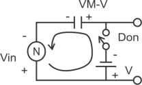
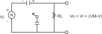
In above diagram during positive half cycle diode will remain permanently off therefore .the job of the diode is only to charge the capacitor.
Vo=vc+vi
Vo=(vm-v)+vi
Series clipper CKT:-
1)Series Negative clipper :- Ideal diode
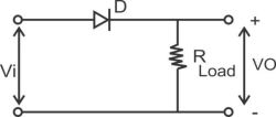
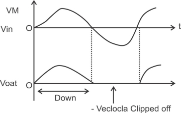
Operation:-
In the positive half cycle of the sinusoidal ilp the diode is forward biased. Being an ideal diode , it acts as a closed switch & connects the load across the ilp the load vtg there fore equal to the vtg in the positive half cycle.
In the –ve half cycle of the diode is reverse biased acts as an open ckts/w the load vtg is therefore zero during the –ve half cycle.
2) Series Positive clipper:-

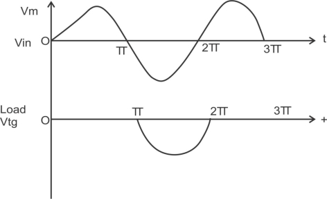
Series clipper with a D.C supply biased [clippers] :-
1) Biased Series –ve Clipper:-
2)

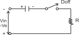
Operation:-
The operation of this ckt can be divided in to there intervals
1) Operation when in is +ve but less than v:-in the positive half cycle of the ilp as long as vin v the diode is not forward biased, therefore from to and then from t2 to t/2 shown in fig below the diode will remain in off state and the o/p voltage will be zero.

Fig -a)Equivalent ckt for +vin>v -
-

Fig b) Equivalent ckt for vin -ve
*BJT:-The BJT is constructed with the three draped semiconductors region’s separate by two Pn junctions as shown below
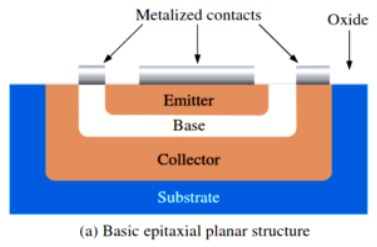
-Basic epitaxial planner structures.
-Three terminal with region’s are called emitter, base and collector.
-The physical representation of the two types of BJT’s,
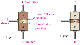
One type consists between two regions separated by a P region (npn) and other type consists of two p regions separated by an n region (pnp).
-The Pn junction joining the base region and the emitter region is called the base emitter junction.
-The Pn junction joining the base region and the collector region is called the base collector junction.
-The base region is lightly doped and very thin compared to the heavily doped emitter and the moderately doped collector regions.
*Base Transistor Operation:-
In order for the transistor to operate properly as an amplifier the two pn junction must be correctly biased with the external D.C vtg.
-The next figure shows the proper bias arrangement for both the npn and pnp transistors for active operation as an amplifier.
-In both the cases the base emitter
(BE) junction is forward biased & the base collector junction (BC) junction is reverse biased
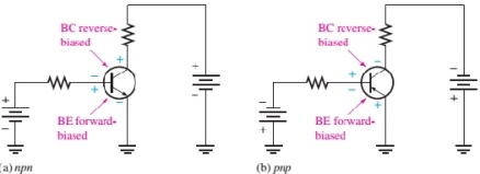
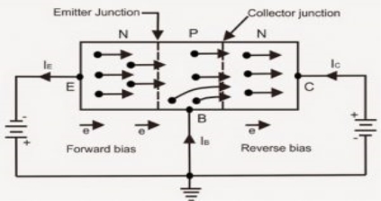
- As from above figure consider n-p-n transistor. The forward bias from base to emitter narrow’s the BE depletion region and the reverse bias from base to collector widens the BC depletion region shown in figure.
- The heavily doped N-TYPE emitter region is full with conduction band(frep) electron’s that easily diffuse through the forward biased BE junction into the p-type base region where they become minority carrier’s same as forward biased diode region
- The base region is lightly doped & very thin so that it has a very limited number of holes.
- Those only a small percentage of all the e-flowing the BE junction can combine with the available holes in the base.
- The relatively few recombined flow out of the base lead as valance electrons, forming as small base current.
- Most of the e flowing from the emitter into the thin lightly dooped base region do not recombine but diffuse into the BC depletion region.
- The BC depletion region diffuse e is being pulled across the reverse biased BC junction by the attraction of the collector supply vtg.
- The electrons now move through the collector region, out through the collector lead into the +ve terminal of the collector vtg source. This forms the collector electrons current.
- The collector current is much larger than the base current.
- This is the reason transistor exhibit current gain.
Transistor Current:-
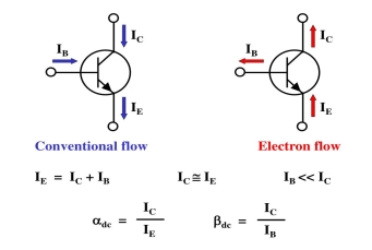
Transistor’s Characteristic’s and parameters:-
-The transistors is connected to d.c bias vtg for both the npn&pnp types VBB forward biases the base emitter junction &Vcc reverse biases the base collector junction.
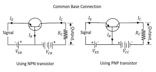
*Biasing conditions for different regions of operation:-
Sr. No | Region of operation | BE junction | CB junction | Work |
1 | Cutoff region | R.B | R.B | S/w |
2 | Active region | F.B | R.B | Ampr |
3 | Saturation region | F.B | F.B |
|
Transistor’s Configuration:-
1) Common Base configuration(C.B)
2) Common emitter Configuration(C.E)
3) Common Collector Configuration(C.C)
Common Base configuration(C.B):-

-The I/p is applied between the emitter and the base. The base acts as a common terminal between the I/p and o/p.
-The input vtg is therefore VEB and the input current is IE.
-The output is taken between the collector and the base therefore the output vtg is VCB and the output current is IC.
* Current relation’s in CB configuration:-
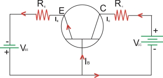
-The collector current is IC of the common base configuration is given by
Ic=Ic(INI)+ICBO
-Where the Ic(INI) called the injected collectors current and it is due to the number of electrons crossing the collectors base junction.
-ICBO :- This is the reverse saturation current flowing due to the minority carrier’s between the collector and base when the emitter is open
-ICBO flow’s due to the reverse biased collector’s base junction. As ICBO negligible as compared to Ic(INI) we can neglect it in practice.
.’. Ic=Ic(INI)………………………practically
Ic=ICBO………………with emitter open
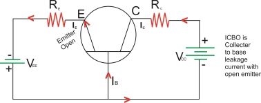
 Emitter is open
 ICBO
ICBO
Collector is to base control
-Since the ICBO flow’s due to terminally generated minority carrier’s it increases with increase the temperature.
-It doubles it’s value for every 100c rise in temperature.
-Current amplification factor or current gain (ddc):-
Current amplification factor or current gain is the ratio of collector current due to the injection to the total emitter current
αd.c = Ic(INI)
-The value of the ddc for CB configuration will always be less than 1.This is because
Ic(INI)<IE.
-Typically the value of d.d.c ranges between 0.95 to 0.995 depending upon the thickness of the base region.
-Larger the thickness of the base region smaller the value of the d.d.c
Ic(INI)=d.d.c.IE
Hence the expression for IC is given by
IC=αd.c IE + ICBo--------------------I
But the ICBo is negligibly small
IC d.d.c IE
* Expression for IB:-
IE=IB+IC
IE=αd.cIE+ICBo+IB…………………from I
IB=(1-αd.c)IE-ICBo
Neglecting ICBo
IB=(1-αd.c)IE
- Characteristics of a transistors in a common base configuration:-
1. Input Characteristic:-
A. Input Characteristic: is always a graph of input current verses input vtg. For common base (CB) configuration input current is the emitter current (IE) & I/p vtg. Is the emitter to the base vtg (VEB)
The I/p Characteristic is plotted at a constant O/p vtg. VCB
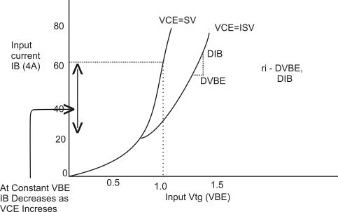
B. Output Characteristic:
Output Characteristic is always a graph of O/p current versus O/p Vtg.
For the CB configuration the O/p current is collector current (IC) of the output voltage is collector to base vtg. (VCB)
Output Characteristic is plotted for a constant value of I/p current (IE)
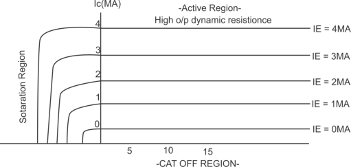
O/p Characteristic of a n-p-n transistor in CB Configuration
Dynamic O/p resistance (ro)
Ro =  / I
/ I  constant
In the active region Ic does not depend on VCB. It depends only on the I/p current IE. That is why the transistor is called as a current controlled or current operated device.
Feature of CB configuration :
- Common terminal : base
- Input current : IE
- O/p current IC
- I/P Vtg. : VEB
- O/P Vtg. VCB
- Current gain :
 ( less than 1)
 - Vtg. Gain : medium
- Input resistance : very low (20-)
- O/P resistance : very high (1 m-2)
Application : as preamplifier
Common Emitter (CE) configuration
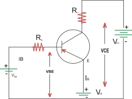
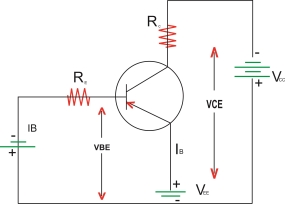
The important points about the CE
Configurations are as follows: the emitter acts as a common terminal between I/p and output. The /p Vtg. Is called between base and emitter
Hence VBE is the I/p Vtg. And IB is the input current.
The O/p is taken between the collector and emitter. There for VCE is the O/p Vtg. And IC is the O/p current.
In order to operate the transistor in its active region the base emitter (BE) junction is forward biased and collector base junction is reverse biased.
- Current relations in CE Configuration:
IE = IC + IB
Where IC =  d.c.IE + ICBO
Rearrange this eqn to get
IC – ICBO =  d.c.IE
 -
-  = IE = IC + IB
 ] = IB -
IC  ] = IB +
 ] +
] + 
- Current gain
 : as
: as  is the ration of o/p current TC and I/p current IB it called common emitter current amplification factor or simply current gain. Thus transistor acts as current amplifier.
The value of  is match higher than
 =
= 
 =
=  =
=  =
= 
IC =  IB +
IB +  …….. I
But  =
= 
 1 +
1 +  =
=  + 1
+ 1
1 +  =
= 
 1 +
1 +  =
= 
Put in eqn I
IC =  IB + (1+
 ICBO above eqn can be expressed as
IC =  IB + ICEO
Where ICEO is the reverse saturation current for the CE configuration which is given by
ICEO = (1+  ) ICBO
- Reverse leakage current :
The Reverse leakage current of a transistor operating
In the LE configuration is denoted by
ICEO = (1 +  ) ICBO
As the value of 
- Match greater than 1 ICEO >>>> ICBO
- As IC =

Put IB = 0
 IC = (1 +
The Reverse leakage current (ICEO)
Increases with increase in the temperature this current flows in the same direction as that of IC there for the collector current IC will increase with increase in temperature even when IB is constant
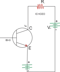
This is called as thermal instability so in CE configuration thermal stabilizing CKT must be included.
- Relation between IC and IB (Current gain
 )
)
We know that
IC 
Though ICEO is large it is much smaller as compared to . Therefor the eqn for IC gets modified as
 C =
C = 

- Relation betn
 &
& :
:
We know that
 but
but
 =
=  =
= 
 =
= 
Similarly we can obtain the expression for  d.c in terms of
  as follows
 d.c =
d.c =  but
but 
=
Multiply & divide numerator & denominator for by IE
 d.c =
d.c = 
 d.c =
d.c = 
 =
= 
- Impact characteristics :

The value of dynamic input resistance ri is low for the CE configuration but it is not as low as that of CE configuration
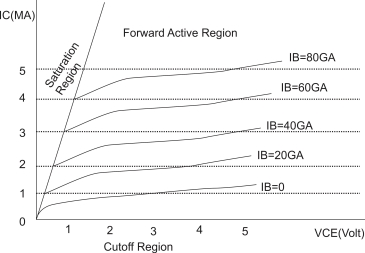
- Cutoff region: Both the BE & CB junctions are reverse biased to operate the transistor in cutoff region. The base current IB = 0 & the collector current is equal to the reverse leakage ICEO. The region below the characteristics for
IB = 0 is cutoff region.
- Active region : the BE emitter junction is forward biased CB junction is reverse biased to operate the transistor in the active region
The collector current IC increases slightly with increase in the vtg.VCE. However the collector current is largely dependent on the base current IB
At fixed value of VCE if IB is increased then it will cause IC to increase substantially.
This is because IC = BIB this relation is true only for the active region of operation.
- Saturation region : the BE junction as well as the collector junction must be forward biased to operate the transistor in its saturation region
- Dynamic o/p resistance
 / constant IB
MOSFET : is another type of field effect transistor. The MOSFET has become one of the most important devices used in design and construction computers
MOSFET [metal oxide semiconductor field effect transistor]
Type of MOSFET
- Depletion type MOSFET
- Enhancement type MOSFET
- Power MOSFET
Enhancement type MOSFET : classified in to two type n. Channel or p. Channel E MOSFET
A) N-channel E MOSFET
B) P-channel E MOSFET
N-channel E MOSFET
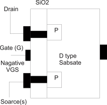
- A slab of P-type semiconductor is used as substrate. The substrate is sometimes connected to the source otherwise it is brought out as the fourth terminal.
- The drain and source terminal are connected to the n-type doped regions through the metallic contacts.
- The insulating sio2 layer is still present which isolates gate terminal from the substrate.
Effect of the insulting sio2 layer :
Due to the presence of the sio2 layer between gate terminal and n-type channel the i/p impedance of MOSFET is very high this is a desirable fracture of a MOSFET. Due to high i/p impedance the gate current IG= 0 for the d.c operating conditions.
Operation : the operation can be explained with two different operating
- Operation with VGS = 0
- Operation when VGS is +ve
1) Operating with VGS = 0 Volt
If VGS = 0 and a positive voltage is applied between its drain and source then due to the absence of the n-type channel a zero drain current will result.
2) Operation when Vgs Positive :
The positive potential at the gate terminal will repel the holes present in the p-type substrate.
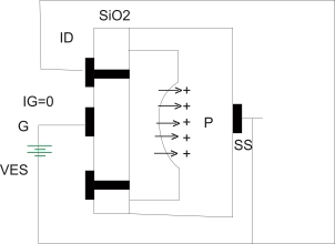
Formation of induced channel in n-channel enhancement MOSFET
This creates a depletion region near the sio2 insulating layer. But the minority carriers ie the electrons in the p-type substrate will be attracted towards the gate terminal and gather near the surface of sio2 as shown above
As we increase the positive VGS the number of e- gathering near the sio2 layer increasesto such an extent that it creates an induced n-channel which connects the n-type doped regions.
The drain current then starts flowing through this induced channel. The value of VGS at which this conduction begins is called as the threshold Vtg. & is indicated.
V-I Characteristics
Characteristics of n-channel enhancement type MOSFET :
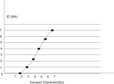
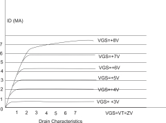
Transfer characteristics drain characteristics
P-channel enhancement type MOSFETS :
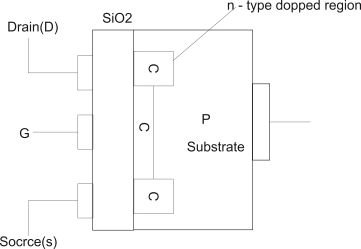
The construction of p-channel EMOSFET is exactly opposite to that of a n-channel EMOSFET
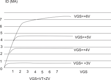
Characteristics:
Drain Characteristics of transfer Characteristics of p-channel E MOSFET
Regions Of Operation, MOSFET As Switch & Amplifier
Operation : the operation can be explained with two different operating
Operation with VGS = 0
Operation when VGS is +ve
Operating with VGS = 0 Volt
If VGS = 0 and a positive voltage is applied between its drain and source then due to the absence of the n-type channel a zero drain current will result.
Operation when Vgs Positive :
The positive potential at the gate terminal will repel the holes present in the p-type substrate.

Formation of induced channel in n-channel enhancement MOSFET
- This creates a depletion region near the sio2 insulating layer. But the minority carriers ie the electrons in the p-type substrate will be attracted towards the gate terminal and gather near the surface of sio2 as shown above
- As we increase the positive VGS the number of e- gathering near the sio2 layer increases to such an extent that it creates an induced n-channel which connects the n-type doped regions.
- The drain current then starts flowing through this induced channel. The value of VGS at which this conduction begins is called as the threshold Vtg. & is indicated.
Effect of increase in the drain to source Vtg. :

Effect of changes in VDS at fixed VGS on the channel width
- The positive gate to source voltage VDS is kept constant and the drain to source voltage VGS is increased gradually.
- Due to this the gate terminal becomes less and less positive with respect to the drain so less number of electron are attracted towards gate terminal & the induced channel becomes narrow.
- Eventually the channel width will be reduced to a point of pinch off and the saturation condition will be established which is same as that in a JFET
- That means any further increase in VDS at the fixed value of VGS will not affect the saturation level of ID unless breakdown condition are encountered.
- Symbols :
1) N-channel EMOSFET 2) P-channel EMOSFEJ
BJT is a bipolar device [minority & majority carriers both contributes to the current flow]
E MOSFET is a unipolar device ie current flows only due to the majority carriers
BJT thermal runaway can damage BJT thermal runway does not take place.
BJT low i/p impedance, E MOSFET High i/p impedance
- Voltage ampɤ :
- Current and vtg gain
Current gain AI is defined as the ratio of o/p current

Vtg gain is given by
Av = Vo/Vi


In this expression if Ro is very small as compared to RL then Av A
A
Thus we can say that the overall gain of the ampɤie Av will approach its open circuit value A if Ro << RL
Prob : An amplifier has a signal i/p Vtg. Vi of 0.25v and draws 1mA from the source. The amɤ delivers & v to a load at 10 mA. Determine the current Vtg and power gains. Also find the i/p resistance of this ampɤ what must be the open ckt. Vtg of the source Vs to provide an ampɤ i/p VtgVi of 0.25 v when the internal resistance of the source is 50 Ω?
Given Vi = 0.25v, Ii = 1 Ma, Vo = 8 v, Io = 10 mA, Rs = 50 Ω.
Solution:
Vtg gain Av = 
Current gain =
= 
Power gain AP = Av  = 32
= 32 
Input resistance Ri =  = 250
= 250
Open circuit Vtg of Vs
Vi = 
Vs = 
Vs = 
Vs = 0.3v
MOSFET as switch :
- MOSFET can act as a switch jest like a transistor a typical switching Ckt using N-channel EMOSFET shown below
- A positive going i/p pulse (high i/p) turns on the EMOSFET. Maxm drain current flows and the o/p Vtg drops from +VDD to RD ID (on). So the EMOSFET acts as closed switch.
- Similarly when the i/p is low (zero) no drain current and hence the o/p is equal to +VDD. So the EMOSFET acts as open s/w
EMOSFET as an AMP :
The purpose of amplifier is to amplify the weak signal faithfully. For amplification MOSFET should operate in a saturation region.
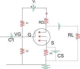
N-channel E-MOSFET Ampɤ
- It can operate with positive gate and drain Vtg where as in p-channel with –ve gate and drain Vtg
- For amplification MOSFET should operate in saturation region where the drain current
 remains constant
 - The threshold Vtg (VT) is the minimum gate Vtg (VGS) required to induce the channel between source to drain
- Fig shows single stage common source ampɤ using Vtg bias method
- Vin is A.c. Signal
- Resistors R1 ,R2 and R5 provides the proper and stabilized operating point
- C in i/p coupling capacitor where is coat is the o/p coupling capacitor which blocks the d.c signal
- Cs is the bypass capacitor so that signal available at source terminal. Never pass through Rs otherwise o/p Vtg reduces.