UNIT 1
Molecular structure and Theories of Bonding
Atomic Orbitals is the mathematical function which is responsible for the determination of location and wave like behavior of an electron in the atom. Atomic orbital is the region where the electrons are present in the atoms. Hence the orbitals in an atom is identified from their unique values i.e.; n, l, m.
Properties:
- Electron orbits the nucleus as a standing wave.
- The electron is at the random position means they never stay at a single position.
Molecular Orbital is the mathematical function which is responsible for the determination of location and wave like behavior of an electron in the molecule. In molecular orbital, the electrons are allowed to interact with more than one atomic nucleus at a time.
The approximate method used to represent molecular orbital is called as the Linear Combination of Atomic Orbital. It is a quantum superposition of atomic orbital and a technique for calculating molecular orbital in quantum chemistry.
Rules for the Linear Combination of Atomic Orbital are:-
- The combining atoms should have the same symmetry along the molecular axis for proper combination. e.g. All the sub-orbitals of 2p have same energy but still, the 2pz orbital of an atom can only combine with a 2pz orbital of another atom but cannot combine with 2px and 2py orbital as they have a different axis of symmetry.
- The two atomic orbital will combine to form molecular orbital. Greater is the extend of overlap of atomic orbital; greater will be the nuclear density.
- The combining atomic orbital must be of equal energy or approximately same energy.
The molecular orbital theory of diatomic molecule can be considered as by taking the H2 molecule in consideration. The molecular orbital are made up of symmetric (both the hydrogen atom are stretched toward the same side) or asymmetric (both the hydrogen atom are stretched toward the opposite side) combination of the 2 atoms to their 1s atomic orbital. According to Molecular Orbital Theory the 1s orbital combine together to form the 2 new molecular orbital of the same Hydrogen molecule with one of it having a lower energy state than the 1s orbital. This MO is denoted by (σ1s and σ*1s). The molecular orbital with higher energy are called as bonding molecular orbital while the other orbital is anti-bonding molecular orbital.
MO Energy level Diagram for Homonuclear Diatomic molecules:
H2 molecule
H2 molecule consist of two H atoms and their two electrons. Two 1s orbitals give two MOs- one bonding that is σ and another one is antibonding that is σ*. The bonding orbital is in lower in energy state, the two electron occupies the bonding MO. The MO electron configuration of H2 molecule is written as (σ1s2).
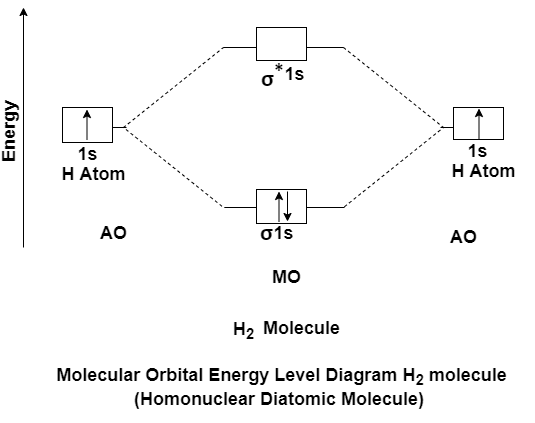
Energy evolved =
[No. Of electron in BMO (-) + No. Of electron in Anti Bonding Molecular Orbital * (+)]
=2*(- ) + 0*(+ )
= -2
This evolved energy is called as stabilization energy.
The molecule is stable so it is diamagnetic.
MO Energy level Diagram for Heteronuclear Diatomic molecules:
Carbon Monoxide Molecule (CO)
CO is the heteronuclear diatomic molecule. This molecule is formed by the combination of carbon and oxygen atom. Electronic configuration of carbon atom is 1s2, 2s2, 2p2 and that of oxygen is 1s2, 2s2, 2p4
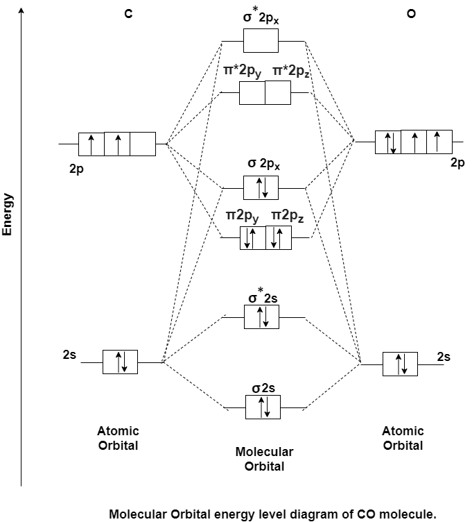
Stabilization Energy
[No. Of electron in BMO * (-) + No. Of electrons in anti bonding molecular orbital * (+)]
= (8) * (-) + (2) * (+)
= -6
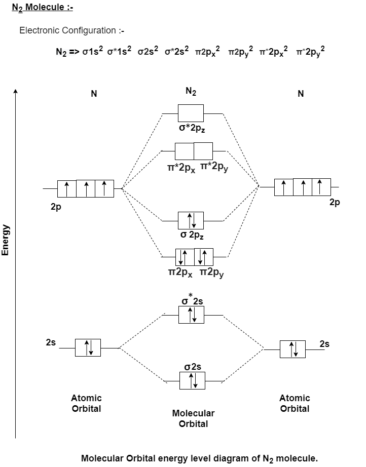
N2 Molecule: -
O2 Molecule:-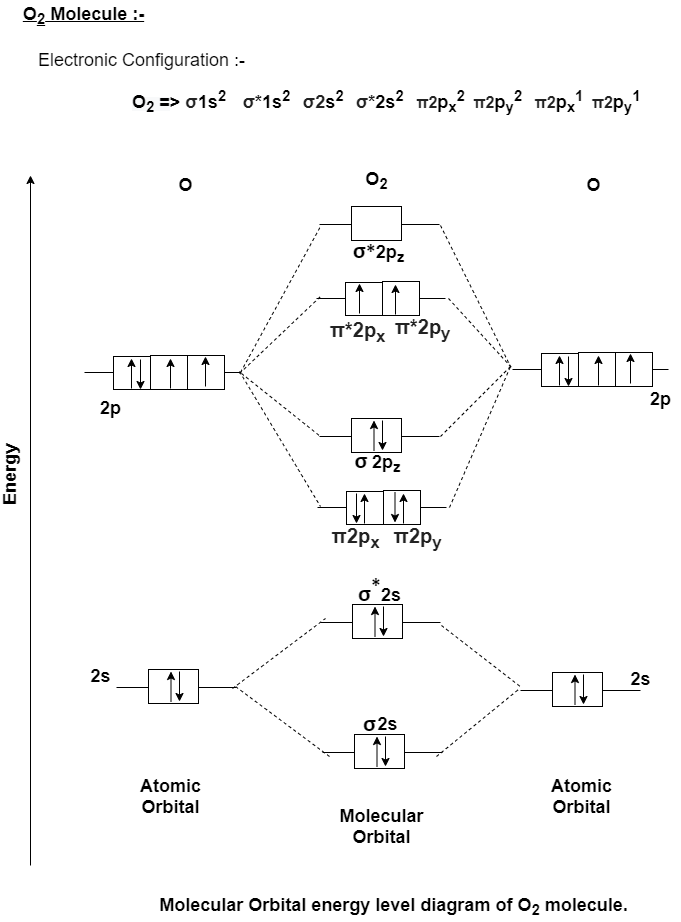 F2 Molecule:-

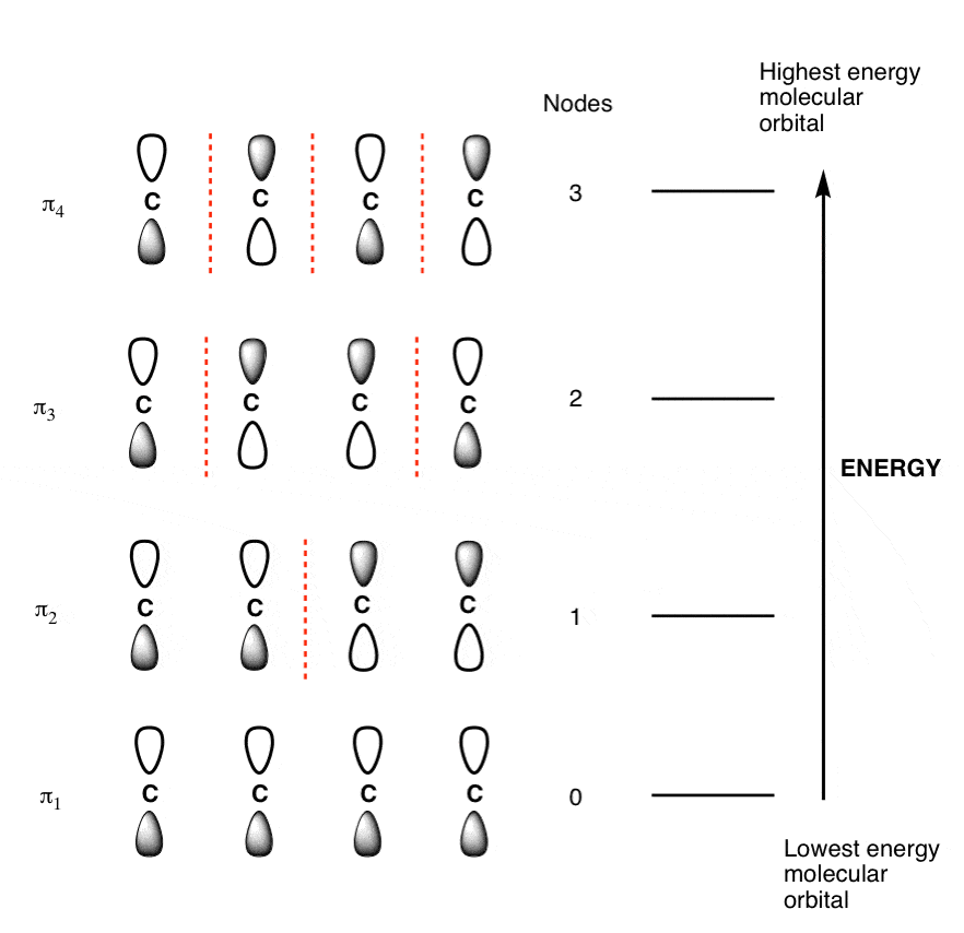
- The number of contributing p-orbital is equal to the number of molecular orbitals for a pi-system.
- The lowest-energy orbital always has zero nodes between the p-orbital.
- At each successive energy level the number of nodes between p-orbital increases by 1.
- The lowest and highest energy orbital are always the easiest pi molecular orbital to draw.
π molecular orbital of butadiene:
The Butadiene Pi System has zero nodes at its lowest energy molecular orbital.

The Butadiene Pi System has three nodes at its lowest energy molecular orbital. The drawn n-p orbital are at alternate phase to each other. This create a pi system with three nodes.

The Butadiene second lowest energy molecular orbital has one node.
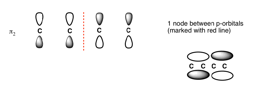
The third lowest energy molecular orbital has two nodes.

The Full Molecular Orbital Diagram for The Butadienyl System.
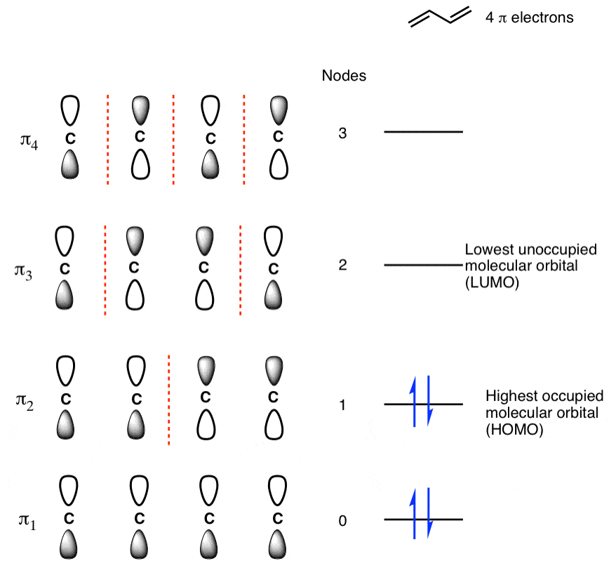
Populating the Molecular Orbitals of Butadiene with Electrons
π molecular orbital of benzene:
The Pi molecular orbital diagram for Benzene

In the above increasing energy level the bottom three orbital are all bonding orbital while the top 3 orbital are anti bonding orbital. The Benzene System has zero nodes at its lowest energy molecular orbital.
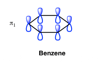
- All p orbital are aligned with phases pointing in the same direction.
- Nodes are absent between orbital.
- In this orbital, electrons are delocalized over the length of molecule, resulting in greatest lowering of energy.
Benzene Has Nodal Planes. The Maximum Energy Level Has 3 Nodal Planes
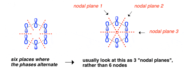
This orbital has zero overlap between adjacent p orbitals and therefore electrons in this orbital have the minimum possible delocalization. They are therefore the highest energy.
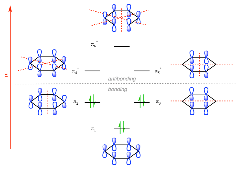
The pi molecular orbital of benzene
On attraction of positively charged metal cation and the negative charge on the non-bonding electrons of the ligand the interaction between a transition metal and ligands arises.
As a ligand approaches the metal ion, the electrons from the ligand will be closer to some of the d-orbitals and farther away from others, causing a loss of degeneracy. The electrons in the d-orbitals and those in the ligand repel each other due to repulsion between like charges. Thus the d-electrons closer to the ligands will have a higher energy than those further away which results in the d-orbitals splitting in energy.
The splitting can be affected by following factors:-
• Metal ion nature
• Metals oxidation state.
• Ligand arrangement around the metal ion
• Metal coordination number
Spectrochemical Series: The ability of ligands to cause a large splitting of the energy between the orbital is essentially independent of the metal ion and the spectrochemical series is a list of ligands ranked in order of their ability to cause large orbital separations.
I- < Br- < SCN- ~Cl- < F- < OH- ~ ONO- < C2O42- < H2O< NCS- < EDTA4-<NH3 ~ pyr ~ en < bipy < phen < CN- ~ CO
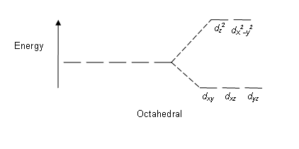
Octahedral: The crystal field stabilization energy (CFSE) is the stability that results from placing a transition metal ion in the crystal field generated by a set of ligands. It arises due to the fact that when the d orbitals are split in a ligand field, some of them become lower in energy than before. For example, in the case of an octahedron, the t2g set becomes lower in energy. As a result, if there are any electrons occupying these orbitals, the metal ion is more stable in the ligand field by the amount known as the CFSE. Conversely, the eg orbitals are higher in energy. So, putting electrons in them reduces the amount of CFSE.
Square Planar: Crystal field stabilization is applicable to the transition-metal complexes of all geometries. The reason that many d8 complexes are square-planar is the very large amount of crystal field stabilization that this geometry produces with this number of electrons.
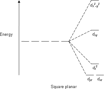
E.g.; XeF4, PtCl2−
Tetrahedral:
dxy dxz dyz
The electron density (i.e., the lobes of the orbitals) lies nearest to the point charges.
dx2-y2 dz2
The electron density lies further away from the point charges.

E.g.; CH4
Band Structure of solids theory is clearly explained by the Molecular Orbital Theory. In Molecular Orbital Theory the number of atomic orbital’s combine to form the same number of molecular orbital so if 2 atomic orbital combine together then they will form 2 molecular orbital these 2 molecular orbital thus formed will be at the lower and higher energy level. If the 2 electrons are filled at lower energy level then it is called the valence band while the vacant anti bonding molecular orbital is called as the conduction band. So, when the electron moves to the anti-bonding molecular orbital from bonding molecular orbital due to the supply of enough energy then this trend in the result of conduction of electricity. E.g.; Taking the Li2 molecule in consideration its valence shell electron 2s2 orbital which gives the molecular orbital
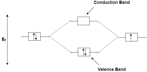
Where, Ef= Fermi Energy
On the supply of equal or little more energy than that of Fermi Energy then one of the paired electrons from the valence band is excited to the conduction band then that electron become responsible for the conduction from one molecule to another molecule.
Insulators: the solids formed by systems such as rare gas atoms, all the bands are completely filled with electrons and the unfilled bands are fully empty. There is no discernible movement of these electrons when the system is subjected to an external electric field and the substance behaves as an insulator. The insulators are those material which does not conduct electricity. As the Fermi energy (Ef=infinite) hence the e- from valence band cannot be excited to the conduction band i.e.; insulators does not conduct electricity.
Semi-conductors: The valence band is completely filled and the upper or the conduction band is empty and the conductivity is negligible. This is similar to diamond except that the gap between the occupied valence band and the higher unoccupied conduction band is small. As the temperature is increased, some levels of the higher band get occupied due to thermal excitation and the system behaves as a conductor.
Effect of Doping on N-type Material
The effect of doping on an N-type material is as follows −
- On addition of Arsenic to pure Silicon, the crystal becomes an N-type material.
- Arsenic atom has additional electrons or negative charges that do not take part in the process of covalent bonding.
- These impurities give up or donate, one electron to the crystal and they are referred to as donor impurities.
- An N-type material has extra or free electrons than an intrinsic material.
- An N-type material is not negatively charged. Actually all of its atoms are all electrically neutral.
- These extra electrons do not take part in the covalent bonding process. They are free to move about through the crystal structure.
- An N-type extrinsic silicon crystal will go into conduction with only 0.005eV of energy applied.
- Only 0.7eV is required to move electrons of intrinsic crystal from the valence band into the conduction band.
Effect of Doping on P-type Material
The effect of doping on a P-type material is as follows −
- When Indium (In) or Gallium (Ga) is added to pure silicon, a P-type material is formed.
- This type of dopant material has three valence electrons. They are eagerly looking for a fourth electron.
- In P type material, each hole can be filled with an electron. To fill this hole area, very less energy is required by electrons from the neighboring covalent bonded groups.
- Silicon is typically doped with doping material in the range of 1 to 106. This means that P material will have much more holes than the electron-hole pairs of pure silicon.
- At room temperature, there is a very determined characteristic difference in the electrical conductivity of this material.