UNIT 2
SEMICONDUCTOR PHYSICS
Semiconductors
Semiconductors are materials that have conductivity between conductors and insulators.
Semiconductors can be pure elements, such as silicon or germanium, or compounds such as gallium arsenide or cadmium selenide.
They are not good conductors nor good insulators as their name “semi”-conductors.
These materials such as silicon (Si), germanium (Ge), and gallium arsenide (GaAs), have electrical properties somewhere in the middle, between those of a “conductor” and an “insulator”.
They have very few “free electrons” because their atoms are closely grouped in a crystalline pattern called a “crystal lattice” but electrons are still able to flow, but only under special conditions.
There are two basic groups or classifications that can be used to define the different semiconductor types:
- Intrinsic Semiconductor
- Extrinsic Semiconductor
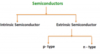
Figure 1: Type of semiconductor
The semiconductor is divided into two types. One is an Intrinsic Semiconductor and the other is an Extrinsic semiconductor. The pure form of the semiconductor is known as the intrinsic semiconductor and the semiconductor in which intentional impurities are added for making it conductive is known as the extrinsic semiconductor.
The conductivity of the intrinsic semiconductor becomes zero at room temperature while the extrinsic semiconductor is very little conductive at room temperature. The detailed explanation of the two types of the semiconductor is given below.
INTRINSIC SEMICONDUCTOR
An intrinsic type of semiconductor material made to be very pure chemically. As a result, it possesses a very low conductivity level having very few charge carriers, namely holes and electrons, which it possesses in equal quantities.
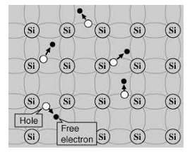
Figure 2: Intrinsic Semiconductor
The most commonly used semiconductor basics material by far is silicon. Silicon has four valence electrons in its outermost shell which it shares with its neighbouring silicon atoms to form a full orbital of eight electrons. The structure of the bond between the two silicon atoms is such that each atom shares one electron with its neighbour making the bond very stable.
As there are very few free electrons available to move around the silicon crystal, crystals of pure silicon (or germanium) are therefore good insulators. Silicon atoms are arranged in a definite symmetrical pattern making them a crystalline solid structure. A crystal of pure silica (silicon dioxide or glass) is generally said to be an intrinsic crystal (it has no impurities) and therefore has no free electrons.
An extremely pure semiconductor is called an Intrinsic Semiconductor. Based on the energy band phenomenon, an intrinsic semiconductor at absolute zero temperature is shown below.
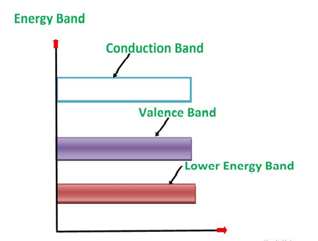
Figure 3: Intrinsic semiconductor at absolute zero temperature.
Its valence band is filled and the conduction band is empty. When the temperature is raised and some heat energy is supplied to it, some of the valence electrons are lifted to the conduction band leaving behind holes in the valence band as shown below.
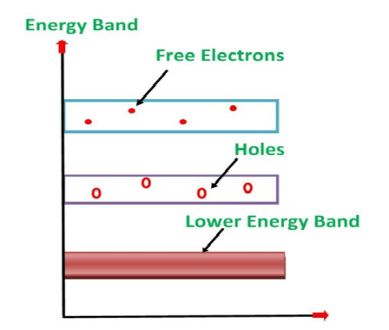
Figure 4: Intrinsic semiconductor at T >0
A hole is the absence of an electron in a particular place in an atom. Although it is not a physical particle in the same sense as an electron, a hole can be passed from atom to atom in a semiconductor material. It is considered to have a positive charge. Holes are positive charge carriers.
The electrons reaching the conduction band move randomly. The holes created in the crystal also free to move anywhere.
This behaviour of the semiconductor shows that they have a negative temperature coefficient of resistance. This means that with the increase in temperature, the resistivity of the material decreases, and the conductivity increases.
But simply connecting a silicon crystal to a battery supply is not enough to extract an electric current from it. To do that we need to create a “positive” and a “negative” pole within the silicon allowing electrons and therefore electric current to flow out of the silicon. These poles are created by doping the silicon with certain impurities.
DOPING
The process by which an impurity is added to a semiconductor is known as Doping. The amount and type of impurity which is to be added to the material have to be closely controlled during the preparation of extrinsic semiconductor. Generally, one impurity atom is added to 108 atoms of a semiconductor.
The purpose of adding impurity in the semiconductor crystal is to increase the number of free electrons or holes to make it conductive.
If a Pentavalent impurity, having five valence electrons is added to a pure semiconductor a large number of free electrons will exist. Which makes an n-type extrinsic semiconductor.
If a trivalent impurity having three valence electrons is added, a large number of holes will exist in the semiconductor. Which makes a p-type extrinsic semiconductor.
EXTRINSIC SEMICONDUCTOR
Extrinsic types of semiconductors are those where a small amount of impurity has been added to the basic intrinsic material. This 'doping' uses an element from a different periodic table group and in this way, it will either have more or fewer electrons in the valence band than the semiconductor itself. This creates either an excess or shortage of electrons. In this way two types of semiconductors are available: Electrons are negatively charged carriers. Holes are positively charged carriers.
Depending upon the type of impurity added the extrinsic semiconductor may be classified as an n-type semiconductor and p-type semiconductor.
P-TYPE EXTRINSIC SEMICONDUCTOR
The extrinsic p-Type Semiconductor is formed when a trivalent impurity is added to a pure semiconductor in a small amount, and as a result, a large number of holes are created in it. A large number of holes are provided in the semiconductor material by the addition of trivalent impurities like Gallium and Indium. Such type of impurities which produce a p-type semiconductor is known as an Acceptor Impurities because each atom of them creates one hole which can accept one electron.
In a P-type semiconductor material, there is a shortage of electrons, i.e. there are 'holes' in the crystal lattice. Electrons may move from one empty position to another and in this case, it can be considered that the holes are moving. This can happen under the influence of a potential difference and the holes can be seen to flow in one direction resulting in an electric current flow. It is harder for holes to move than for free electrons to move and therefore the mobility of holes is less than that of free electrons. Holes are positively charged carriers.
A trivalent impurity like Aluminium, having three valence electrons is added to Silicon crystal in a small amount. Each atom of the impurity fits in the Silicon crystal in such a way that its three valence electrons form covalent bonds with the three surrounding Silicon atoms as shown in the figure below.
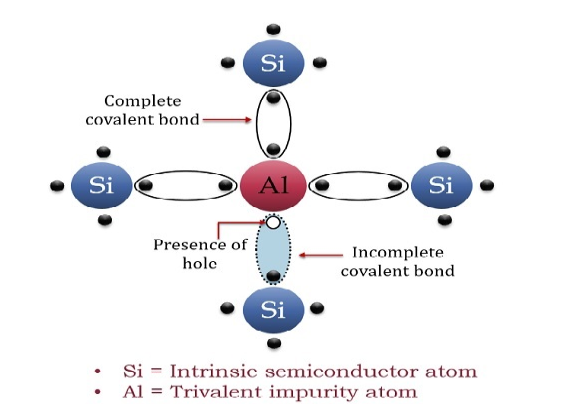
Figure 5: p-Type Semiconductor
ENERGY BAND DIAGRAM OF P-TYPE SEMICONDUCTOR
The energy band diagram of a p-Type Semiconductor is shown below.
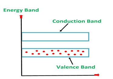
Figure 6: Energy band diagram of a p-Type Semiconductor
A large number of holes or vacant space in the covalent bond is created in the crystal with the addition of the trivalent impurity. A small or minute quantity of free electrons is also available in the conduction band.
They are produced when thermal energy at room temperature is imparted to the Silicon crystal-forming electron-hole pairs. But the holes are more in number as compared to the electrons in the conduction band. It is because of the predominance of holes over electrons that the material is called a p-type semiconductor. The word “p” stands for positive material.
CONDUCTION THROUGH P TYPE SEMICONDUCTOR
In p-type semiconductors, a large number of holes are created by the trivalent impurity. When a potential difference is applied across this type of semiconductors.
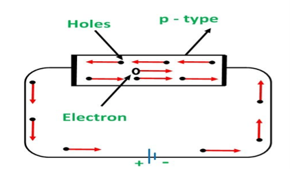
Figure 7: Conduction through p type semiconductor
The holes are available in the valence band are directed towards the negative terminal. As the current flow through the crystal is by holes, which are a carrier of positive charge, therefore, this type of conductivity is known as positive or p-type conductivity. In a p-type conductivity, the valence electrons move from one covalent to another.
The conductivity of an n-type semiconductor is nearly double that of a p-type semiconductor. The electrons available in the conduction band of the n-type semiconductor are much more movable than holes available in the valence band in a p-type semiconductor. The mobility of holes is poor as they are more bound to the nucleus.
Even at room temperature, the electron-hole pairs are formed. These free electrons which are available in minute quantity also carry a little amount of current in the p-type semiconductors.
N-TYPE EXTRINSIC SEMICONDUCTOR
When a few Pentavalent impurities such as Phosphorus whose atomic number is 15, which is categorized as 2, 8, and 5. It has five valence electrons, which are added to silicon crystals. Each atom of the impurity fits in four silicon atoms as shown in the figure below.
Hence, each Arsenic atom provides one free electron in Silicon crystal. Since an extremely small amount of Phosphorus, impurity has a large number of atoms; it provides millions of free electrons for conduction.
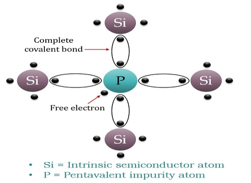
Figure 8: N-type semiconductor
An N-type semiconductor material has an excess of electrons. In this way, free electrons are available within the lattices, and their overall movement in one direction under the influence of a potential difference results in an electric current flow. This is an N-type semiconductor, the charge carriers are electrons.
ENERGY DIAGRAM OF N-TYPE SEMICONDUCTOR
A large number of free electrons are available in the conduction band because of the addition of the Pentavalent impurity. These electrons are free electrons that did not fit in the covalent bonds of the crystal. However, a minute quantity of free electrons is available in the conduction band forming hole- electron pairs.
The Energy diagram of the n-type semiconductor is shown in the figure below.
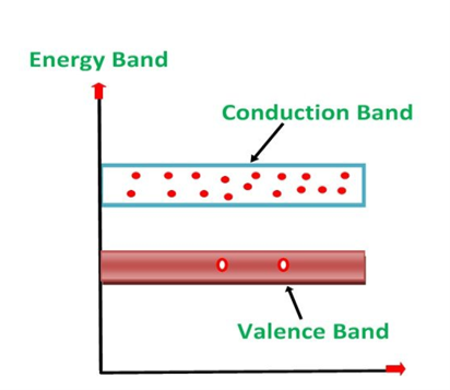
Figure 9: Energy diagram of the n-type semiconductor
- The addition of pentavalent impurity results in a large number of free electrons.
- When thermal energy at room temperature is imparted to the semiconductor, a hole-electron pair is generated and as a result, a minute quantity of free electrons is available. These electrons leave behind holes in the valence band.
- Here n stands for negative material as the number of free electrons provided by the pentavalent impurity is greater than the number of holes.
CONDUCTION THROUGH N-TYPE SEMICONDUCTOR
In the n-type semiconductor, a large number of free electrons are available in the conduction bands which are donated by the impurity atoms. The figure below shows the conduction process of an n-type semiconductor.
When a potential difference is applied across this type of semiconductor, the free electrons are directed towards the positive terminals. It carries an electric current. As the flow of current through the crystal is constituted by free electrons which are carriers of a negative charge, therefore, this type of conductivity is known as negative or n-type conductivity.
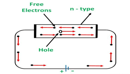
Figure 10: Conduction through n-type semiconductor
The electron-hole pairs are formed at room temperature. These holes which are available in small quantities in the valence band also consist of a small amount of current. For practical purposes, this current is neglected.
Key Takeaways
- Semiconductors are materials that have conductivity between conductors and insulators.
- The semiconductor is divided into two types. One is an Intrinsic Semiconductor and the other is an Extrinsic semiconductor.
- The pure form of the semiconductor is known as the intrinsic semiconductor
- The semiconductor in which intentional impurities are added for making it conductive is known as the extrinsic semiconductor.
- A hole is the absence of an electron in a particular place in an atom.
- The process by which an impurity is added to a semiconductor is known as Doping.
- Depending upon the type of impurity added the extrinsic semiconductor may be classified as an n-type semiconductor and p-type semiconductor.
- The extrinsic p-Type Semiconductor is formed when a trivalent impurity is added to a pure semiconductor in a small amount, and as a result, a large number of holes are created in it.
- The extrinsic n-Type Semiconductor is formed when a Pentavalent impurity is added to a pure semiconductor in a small amount, and as a result, a large number of electrons are created in it.
FERMI ENERGY
Intrinsic semiconductors—carrier concentration
Here we will calculate the number of electrons excited into the conduction band at temperature T and also the hole concentration in the valence band. It is assumed that the electrons in the conduction band behave as if they are free particles with effective mass me* and the holes near the top of the valence band behave as if they are free particles with effective mass mh*.
Here we will calculate the electron concentration, hole concentration
The density of Electrons in Conduction Band
The number of free electrons per unit volume of a semiconductor having energies in between E and E + dE is represented as N(E) dE
dE = width of Energy band
Therefore, we have:
N(E) dE = ge(E) dE fe(E) ……….(1)
ge(E) = The density of electron states per unit volume
fe(E) = Fermi-Dirac distribution function i.e. probability that an electron occupies an electron state
The number of electrons present in the conduction band per unit volume of material ‘n’ is obtained by integrating N(E) dE between the limits Ec and Ect
Where Ec = the bottom energy levels of the conduction band
Ect = the bottom and top energy levels of the conduction band
n =  ……….(2)
Can be written as
n =  =
= 
n =  -
-  ……….(3)
We know that above Ect, there are no electrons.
Hence, Equation (3) becomes
n =  -
- 
n =  ……….(4)
The Fermi-Dirac distribution function fe(E) can be represented as:
 (E) =
(E) = ……….(5)
Compared to the exponential value, so the ‘1’ in the denominator can be neglected.
So  >>1
>>1
Hence,  (E) =
(E) = =
=  ……….(6)
The density of electron states ge(E) in the energy space from E = 0 to E can be written as:
 (E) =
(E) =  [
[ ]3/2 (E - 0) ½ ……….(7)
Where me* is the effective mass of an electron and h is Planck’s constant.
 (E)dE =
  [
[ ]3/2 (E - 0) ½dE ……….(8)
To evaluate n, the density of states is counted from Ec, since the minimum energy state in the conduction band is Ec. So eq (8) can become
 (E)dE =
  [
[ ]3/2 (E - Ec) ½dE ……….(9)
Substituting Equations (6) and (9) in (4) gives
n =  3/2
3/2 (E-
(E- )1/2
)1/2 dE
dE
n = [
[ ]3/2
]3/2  1/2
1/2 dE ………… (10)
The above equation can be simplified by the following substitution:
Put ɛ = E − Ec ………… (11)
So, dɛ = dE
In Equation (11), Ec is constant, as we change the variable E to ε in Equation (10), the integral limits also change.
In Equation (11), as E → Ec then ε → 0 and E → ∞, then ε also → ∞.
The exponential term in Equation (10) becomes:
 = exp [
 ] = exp [
 ]
]

 ………… (12)
Substituting Equations (11) and (12) in (10), we get:
n = [
[ ]3/2
]3/2  dE
dE
n = [
[ ]3/2
]3/2
 dE ………… (13)
Above integral (I) can be simplified by substitution. Put ε = x2
So that dɛ = 2x dx
I = 2x dx
2x dx
= dx
dx
= =
= T)3/2 ………… (14)
Substituting Equation (14) in (13) gives:
n = [
[ ]3/2
]3/2 T)3/2
T)3/2
n =
n = 
n =  ………… (15)
The term  is almost a constant compared with the exponential term as the temperature changes. So, it is a pseudo constant and is given by the symbol Nc. So, we have
n =Nc ………… (16)
The density of Holes in Valence Band
The number of holes per unit volume of semiconductor in the energy range E and E + dE in the valence band is represented as P(E) dE. Proceeding the same way (as in the case of electrons) we have
Therefore, we have:
P(E) dE = gh(E) dE fh(E) ……….(17)
dE = width of Energy band
gh(E) = The density of holes states per unit volume
fh(E) = Fermi-Dirac distribution function i.e. probability that a hole occupies an electron state
The number of electrons present in the conduction band per unit volume of material ‘n’ is obtained by integrating P(E) dE between the limits Evb and EV
Where EV = the bottom energy levels of the valence band
Evb = the bottom and top energy levels of the valence band
The total number of holes present in the valence band per unit volume of material ‘p’ is obtained by integrating P(E) dE
 ……….(18)
Equation (18) can be represented as:
 ……….(19)
Now we know that below Evb no holes are present. Hence, Equation (19) becomes
 ……….(20)
We know a hole can also be defined as the absence of an electron.
Presence of a hole = the absence of an electron
Hence, the Fermi-Dirac function of holes fh(E) in the valence band is:
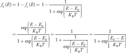
Compared to exponential, the ‘1’ in the denominator is negligible,

Hence,
 ……….(21)
The density of hole states between E and E + dE in valence band can be written similar to Equation (8.9) for electrons.
 ……….(22)
Where mh* is the effective mass of the hole.
Substituting Equations (21) and (22) in (20),
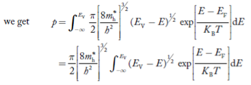 ……….(23)
The above equation can be simplified by the substitution:
Put ɛ = EV − E ............. (24)
So dɛ = − dE
In Equation (24), EV is constant, as we change the variable E to ε in Equation (23), the integral limits also change.
In Equation (24),
As E → EV then ε → 0
And E→ −∞, then ε → ∞
The exponential term in Equation (23) becomes:
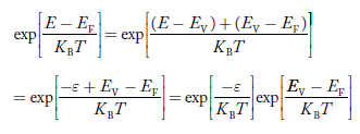 ............. (25)
Substituting Equations (24) and (25) in (23), we get:
 ………….(26)
From Equation (14), we know the integral value  T)3/2 put here and we get
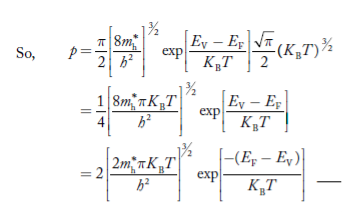 ………….(27)
….The term  is almost constant compared with the exponential term as the temperature changes. So, it is a pseudo constant and is given by the symbol NV. So, we have
 …………… (28)
Fermi Level
We know that in an intrinsic semiconductor
Electron concentration ‘n’ = Hole concentration ‘p’
Equating Equations (15) and (27), we get
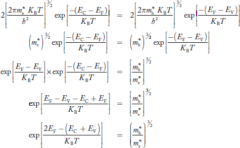
Taking logarithms on both sides, we get
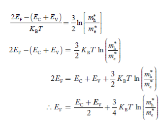 ……………… (29)
Normally, mh* is greater than me*, since ln  is very small so that EF is just lie in the middle of the energy gap
Temperature effect on Fermi level
Fermi level slightly rises with an increase of temperature.
But in the case of a pure intrinsic semiconductor like Si and Ge,
mh* ≈ me*
So in these cases, the Fermi level lies in the middle of the energy gap.
DEPENDENCE OF FERMI ENERGY ON CARRIER CONCENTRATION AND TEMPERATURE (QUALITATIVE)-
Carrier Concentration in Extrinsic Semiconductors
The number of charge carriers presents per unit volume of a semiconductor material is called carrier concentration.
Suppose donor and acceptor atoms are doped in a semiconductor.
At temperature T K,
n = number of conduction electrons
p = number of holes
N−A = number of acceptor ions
N+D = number of donor ions
We know that the below equation holds good in the semiconductor. The total negative charge due to conduction electrons and acceptor ions is equal to holes and donor ions in a unit volume of material.
So the material will be considered neutral if,
n + N−A = p + N+D ……….(34)
Equation (34) is called the charge neutrality equation.
In the above equation
 ………..(35)
Concentration of acceptor ions N−A = acceptor concentration x probability of finding an electron in acceptor level
 ………..(36)
Similarly, the donor ions concentration is

 ………..(37)
In n-type material
Note
nn represents electrons in n-type material
pn represents holes concentration in n-type material.
There are no acceptor atoms so N−A = 0.
At 0 K, all the electron states at the donor level are occupied by electrons.
As the temperature is increased from 0 K, some of the electrons jump from these donor states into the conduction band.
Also, the concentration of holes is extremely less compared with the concentration of conduction electrons [p << n]
From Equation (34) we have
n = p N+D
(Or) n ≈ N+D …………(38) [since p << N+D]
At temperature T K,
As the temperature increase, almost all the donor atoms donate electrons to the conduction band.
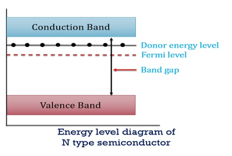
Figure 11: Energy level diagram of N type semiconductor
So, in n-type material, the free electron concentration is almost equal to the donor atoms.
So we can rewrite the above equation as
nn ≈ ND …………….(39)
Where nn represents electrons in n-type material
Also, the hole concentration in n-type material can be obtained by applying the law of mass action nn pn =ni2
 …………..(40)
Where pn represents holes concentration in n-type material.
In n-type material at 0 K, the Fermi energy level lies in the middle of Ec and ED

At temperature> 0K
 ……….(41)
With the increase in temperature, the Fermi level shifts upwards according to Equation (61) slightly due to the ionization of donor atoms.
With further increase of temperature, electron-hole pairs are generated due to the breaking of covalent bonds, hence Fermi level shifts downwards.
In p-type semiconductor
Note
pp represents holes in the p-type material
np represents electrons in the p-type material
There are no donor atoms so means no ions present  = 0.
= 0.
At 0 K, all the acceptor levels are not occupied by electrons.
As the temperature is increased from 0 K, some electrons jump from top valence band energy levels to the acceptor states, leaving holes in the valence band and acceptor ions  are formed.
At some room temperature T K, the concentration of conduction electrons is extremely less compared with hole concentration.
∴ From Equation (34), we have
n + N−A = p ……………(42)
(or) N−A ≈ p ……………. (43) [since n << N−A]
At temperature T K, in p-type material,
The hole concentration is almost equal to the acceptor atoms in a unit volume of the material.
So, Equation (43) can be written as
pp ≈ NA ……………….(44)
Where pp represents holes in the p-type material
The electron concentration in p-type material can be obtained by applying the law of mass action as nppp = ni2
 …………….(45)
Where np represents free electron concentration in the p-type material.
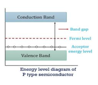
Figure 12: Energy level diagram of N type semiconductor.
In p-type material, the Fermi level lies in between EV and EA at 0 K

As the temperature is increased from 0 K, the Fermi level shifts downwards slightly as per Equation (46) due to ionization of acceptor atoms.
And with a further increase of temperature, electron-hole pairs are generated due to the breaking of covalent bonds, so the Fermi level shifts upwards.
Key Takeaways
- The density of Electrons in Conduction Band
n =Nc
- The density of Holes in Valence Band

- Fermi level slightly rises with an increase of temperature. But in the case of a pure intrinsic semiconductor like Si and Ge, mh* ≈ me*, So in these cases, the Fermi level lies in the middle of the energy gap.
Carrier Concentration in Extrinsic Semiconductors
- The donor ions concentration is
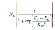
- Concentration of acceptor ions N−A

- Fermi Level shifts in case of extrinsic semiconductor.
Carrier generation is a process where electron-hole pairs are created by exciting an electron from the valence band of the semiconductor to the conduction band, thereby creating a hole in the valence band.
Recombination is the reverse process where electrons from the conduction and holes from valence band recombine and are annihilated.
These processes must conserve both quantized energy and momentum, and the vibrating lattice plays a large role in conserving momentum.
- Recombination and generation are always happening in semiconductors both optically and thermally.
- Their rates are in balance at equilibrium.
- If the product of the rate becomes greater than the recombination rate, again driving the system back towards equilibrium.
- As the electron and hole densities is a constant at equilibrium, maintained by recombination and generation occurring at equal rates.
- When there is a surplus of carriers the rate of recombination becomes greater than the rate of generation, driving the system back towards equilibrium.
In semiconductors several different processes exist which lead to recombination, the most important ones are:
1) Band-to-band recombination
2) Auger generation/recombination
3) Surface recombination
1) Band-to-band recombination or Radiative recombination
Band-to-band recombination or Radiative recombination is the reverse process of photon absorption, where an electron drops back down to its equilibrium energy band and radiates a photon.
It is the process of electrons jumping down from the conduction band to the valence band in a radiative manner.
During band-to-band recombination the energy absorbed by a material is released in the form of photons. Generally these released photons contain the same or less energy than those initially absorbed.
The photon emitted may have the energy of the band gap difference or less, depending on how much energy is lost in the mechanism
Radiative recombination plays a more major role in direct band semiconductors.
The total radiative recombination rate, given below as R, is proportional to the product of the concentration of occupied states (electrons, n) in the conduction band and that of the unoccupied states in the valence band (holes, p)
R= Bnp
Band-to-band recombination depends on the density of available electrons and holes. Both carrier types need to be available in the recombination process. Therefore, the rate is expected to be proportional to the product of n and p. Also, in thermal equilibrium, the recombination rate must equal the generation rate since there is no net recombination or generation. As the product of n and p equals ni2 in thermal equilibrium, the net recombination rate can be expressed as:
U= B(np-ni2)
Where B is the bimolecular recombination constant for a given semiconductor. It can be calculated from the semiconductor’s absorption coefficient. ni2 is the familiar “intrinsic carrier concentration”
Auger recombination
Auger recombination involves three particles: an electron and a hole, which recombine in a band-to-band transition and give off the resulting energy to another electron or hole. The expression for the net recombination rate is therefore similar to that of band-to-band recombination but includes the density of the electrons or holes, which receive the released energy from the electron-hole annihilation.
In other words Auger recombination the energy is given to a third carrier which is excited to a higher energy level without moving to another energy band.
After the interaction, the third carrier normally loses its excess energy to thermal vibrations. Since this process is a three-particle interaction, it is normally only significant in non-equilibrium conditions when the carrier density is very high.
Auger recombination is most important at high carrier concentrations caused by heavy doping. In silicon-based solar cells, Auger recombination limits the lifetime and ultimate efficiency.
The more heavily doped the material is, the shorter the Auger recombination lifetime.
Surface recombination
Recombination at surfaces and interfaces can have a significant impact on the behavior of semiconductor devices.
Areas of defect, such as at the surface of solar cells where the lattice is disordered, recombination is very high.
This is because surfaces and interfaces typically contain a large number of recombination centers because of the abrupt termination of the semiconductor crystal, which leaves a large number of electrically active states.
In addition, the surfaces and interfaces are more likely to contain impurities since they are exposed during the device fabrication process.
The net recombination rate due to trap-assisted recombination and generation is given by:

The recombination is due to a two-dimensional density of traps, Nts, as the traps only exist at the surface or interface.
Understanding the impacts and the ways to limit surface recombination leads to better and more robust solar cell designs. Surface recombination is high in solar cells, but can be limited.
Key Takeaways
- Carrier generation is a process where electron-hole pairs are created by exciting an electron from the valence band of the semiconductor to the conduction band, thereby creating a hole in the valence band.
- Recombination is the reverse process where electrons from the conduction and holes from valence band recombine and are annihilated.
- These processes must conserve both quantized energy and momentum, and the vibrating lattice plays a large role in conserving momentum.
- Recombination and generation are always happening in semiconductors both optically and thermally.Their rates are in balance at equilibrium.
- In semiconductors several different processes exist which lead to recombination, the most important ones are: Band-to-band recombination, Auger generation/recombination and Surface recombination
Drift current and diffusion currents
In case of semiconductors we observe two kinds of currents.
- Drift current
- Diffusion current
Drift current Definition:- The flow of electric current due to the motion of charge carriers under the influence of external electric field is called drift current.
When an electric field E is applied across a semiconductor material, the charge carriers attain a drift velocity vd
So drift velocity vd =μ .E
The relation between current density J and drift velocity vd is
J = Nqvd
Where N is the carrier concentration
q is the charge of electron or hole
From equations (1) and (2), we get
Jdrift = Nq μE
μ is the mobility of charge carrier.
The above equation shows the general expression for drift current density. Drift current density due to electrons is
Je(drift) = neμeE
Where n is the electrons carrier concentration
And μe is the mobility of electrons.
Drift current density due to holes is
Jh(drift) = peμhE
Where p is the carrier concentration of holes.
μh is the mobility of holes
So Total drift current density
Jdrift (total) = Je(drift) + Jh(drift) = neμeE + peμhE
= eE (nμe+pμh )
Diffusion current
Definition:-The flow of electric current due to the motion of charge carriers under concentration gradient is called diffusion current
Or
The motion of charge carriers from the region of higher concentration to lower concentration leads to a current called diffusion current.
Let ∆N be the excess electron concentration. Then according to Fick’s law, the rate of diffusion of charge carriers is proportional to concentration gradient
Rate of diffusion of charge ∝ -
= - D
Where D is the diffusion coefficient of charge carriers.
The negative sign indicates decrease of N with increase of x So,
The diffusion current density Jdiffu is
Jdiffu = - qD
Where q is the charge of the charge carrier
Diffusion current density due to holes is
Jdiffu (hole) = - eDh
Diffusion current density due to electrons is (as electron carry negative charge so we will get +sign here.
Jdiffu (electrons) = eDe
Jdiffu (total) = Jdiffu (hole) + Jdiffu (electrons)
Jdiffu (total) = - eDh + eDe
+ eDe
The expression for total current density due to holes is
Jh (total) = Jh(drift) + Jdiffu (hole) = peμhE - eDh
The expression for total current density due to electrons is
Je (total) = Je(drift) + Jdiffu (electrons) = neμeE + eDe
Key Takeaways
- In case of semiconductors we observe two kinds of currents; Drift current and Diffusion current.
- The flow of electric current due to the motion of charge carriers under the influence of external electric field is called drift current. STotal drift current density is given by Jdrift (total) = Je(drift) + Jh(drift) = eE (nμe+pμh )
- The flow of electric current due to the motion of charge carriers under concentration gradient is called diffusion current. Total current density due to electrons is given by Je (total) = Je(drift) + Jdiffu (electrons) = neμeE + eDe

When the magnetic field is applied perpendicular to a current-carrying conductor, then a voltage is developed in the material perpendicular to both the magnetic field and current in the conductor. This effect is known as Hall Effect and the voltage developed is known as Hall voltage (VH).
Hall Effect is useful to identify the nature of charge carriers in material and hence to decide whether the material is an n-type semiconductor or p-type semiconductor, also to calculate carrier concentration and mobility of carriers.
Hall Effect can be explained by considering a rectangular block of an extrinsic semiconductor in which current is flowing along the positive X-direction and magnetic field B is applied along Z-direction as shown in Figure.
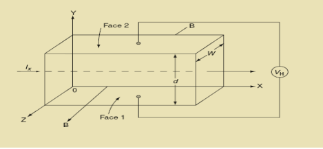
Figure 13: Hall Effect
Suppose if the semiconductor is n-type, then mostly the carriers are electrons and the electric current is due to the drifting of electrons along negative X-direction or if the semiconductor is p-type, then mostly the carriers are holes and the electric current is due to drifting of the holes along positive X-direction.
As these carriers are moving in the magnetic field in the semiconductor that means they experience Lorentz force represented by FL
FL = Bevd
Where vd is the drift velocity of the carriers. (already explained in the previous section).
We can obtain the direction of this force by applying Fleming’s left-hand rule in electromagnetism.
Fleming’s left-hand rule can be explained as If we stretch the thumb, forefinger, and middle finger in three perpendicular directions so that the forefinger is parallel to the magnetic field and the middle finger is parallel to the current direction, then the thumb represents the direction of the force on the current-carrying carriers.
So the Lorentz force is exerted on the carriers in the negative Y-direction. Due to Lorentz force, more and more carriers will be deposited at the bottom face (represented by face 1in the figure) of the conductor.
The deposition of carriers at the bottom face is continued till the repulsive force due to accumulated charge balances the Lorentz force.
After some time of the applied voltage, both the forces become equal in magnitude and act in opposite direction, then the potential difference between the top and bottom faces is equal to Hall voltage and that can be measured.
At equilibrium, the Lorentz force on a carrier
FL = Bevd ……………..(1)
And the Hall force
FH = eEH ……………..(2)
Where EH is the Hall electric field due to accumulated charge.
At equilibrium, FH = FL
EEH = Bevd
∴ EH = Bvd ……………..(3)
If ‘d’ is the distance between the upper and lower surfaces of the slab, then the Hall field
EH =  ……………..(4)
In n-type material, Jx = –nevd
vd = -  ……………..(5)
Where n is free electron concentration, substituting (5) in (3), we have
∴ EH = -B  ……………..(6)
For a given semiconductor, the Hall field EH is proportional to the current density Jx and the intensity of magnetic field ‘B’ in the material.
i.e. EH ∝ JxB
(or) EH = RHJxB ……………..(7)
Where RH = Hall coefficient
Equations (6) and (7) are the same so, we have
RHJxB =-B 
RH = -  = -
= -  ……………..(8)
Where ρ is the charge density
Similarly for p-type material
RH =  =
= ……………..(9)
Using Equations (8) and (9), carrier concentration can be determined.
Thus, the Hall coefficient is negative for n-type material. In n-type material, as the more negative charge is deposited at the bottom surface, so the top face acquires positive polarity and the Hall field is along negative Y-direction. The polarity at the top and bottom faces can be measured by applying probes.
Similarly, in the case of p-type material, a more positive charge is deposited at the bottom surface. So, the top face acquires negative polarity and the Hall field is along positive Y-direction. Thus, the sign of the Hall coefficient decides the nature of (n-type or p-type) material.
The Hall coefficient can be determined experimentally in the following way:
Multiplying Equation (7) with ‘d’, we have
EHd = VH = RHJxBd ……………..(10)
From (Figure 13) we know the current density Jx
Jx = 
Where W is the width of the box. Then, Equation (10) becomes
VH = RH Bd = RH
RH =  ……………..(11)
Substituting the measured values of VH, Ix, B, and W in Equation(11), RH is obtained. The polarity of VH will be the opposite for n- and p-type semiconductors.
The mobility of charge carriers can be found by using the Hall effect, for example, the conductivity of electrons is
n = neμn
Or we can rewrite it as
μn =  =n RH ……………..(12)
By using equation (11)
μn = n ……………..(13)
Applications of Hall Effect
• Using magnetic flux leakage – To properly inspect items such as pipes or tubes, Hall Effect probes work with something called magnetic flux leakage. This is a way of testing such items, and being able to spot potential corrosion, erosion, or pitting. This is specifically used in steel items and can give important information about lifespan or safety.
• Sensors to detect rotation speed – A Hall Effect probe can be used in bicycle wheels, speedometers in the automotive world, electronic types of ignition systems, and gear teeth.
• Used to detected movement – You will often find a Hall Effect probe used in such items as Go-Kart controls, smartphones, paintball guns, or airsoft guns, as well as some GPS systems.
• Ferrite Toroid Hall Effect current transducers – This is mainly used in electronic compasses, making use of the magnetic field to show direction.
• Split-ring clamp-on sensors – These types of Hall Effect probes are used to test equipment without having to take the whole circuit board apart, e.g. Complex items.
• Analog multiplication – Anything which needs a power measurement, e.g. Sensing, and is also used in small computers.
• General power measurement – Any device which needs to be tested for its power input can be done by a Hall Effect probe.
• Position and motion sensors – This is mainly used in a DC motor, often the brushless type.
• The automotive world – Hall Effect probes are used widely in the automotive world, especially in fuel injection and ignition. Wheel rotation sensors also use Hall Effect probes, e.g. For anti-lock braking.
- For determination of the type of given semiconductor.
- For N-type, Hall coefficient RH= negative
- For P-type, Hall coefficient RH= Positive
- To determine carrier concentration n and p; that is n=p=1/e𝑅𝐻
- Determination of mobility of charge carriers μn =
 =n RH. Where 𝜎= electrical conductivity
 - To determine the sign of charge carriers whether the conductivity is due to electrons or holes.
Main Advantages of Using Hall Sensors
Why is a Hall Effect probe advantageous in all of these instances? Because the probes are not affected by outside influences, e.g. Water or dirt. They can also easily sense the measure of the output they need when they are placed in the right position. On top of this, Hall Effect probes are safer, because the voltage never actually makes it directly to the sensor/probe. This makes this type of measurement overall so much safer than other methods.
As you can see, understanding how something is put into practice in the real world helps you to understand it in real terms. The Hall Effect is certainly very commonplace these days, in much more methods and applications than we realize. While certainly very useful in the automation world, even basic items such as a compass make large use of this scientific approach.
Key Takeaways
- When the magnetic field is applied perpendicular to a current-carrying conductor, then a voltage is developed in the material perpendicular to both the magnetic field and current in the conductor. This effect is known as Hall Effect.
- The voltage developed is known as Hall voltage (VH).
- Hall Effect is useful to identify the nature of charge carriers in material and hence to decide whether the material is an n-type semiconductor or p-type semiconductor.
- Hall Effect also to calculate carrier concentration and mobility of carriers.
- Hall coefficient is given by RH = -
 = -
= -  Where ρ is the charge density
 - Hall coefficient is given by RH =

- Mobility of charge carriers can be found by using the Hall Effect μn = n

A P-N Junction Diode is formed by doping one side of a piece of silicon with a P-type dopant (Boron) and the other side with a N-type dopant (phosphorus). Ge can be used instead of Silicon. The P-N junction diode is a two-terminal device. This is the basic construction of the P-N junction diode. It is one of the simplest semiconductor devices as it allows current to flow in only one direction.
ZERO BIASED CONDITION
In this case, no external voltage is applied to the P-N junction diode; and therefore, the electrons diffuse to the P-side and simultaneously holes diffuse towards the N-side through the junction, and then combine with each other. Due to this an electric field is generated by these charge carriers. The electric field opposes further diffusion of charged carriers so that there is no movement in the middle region. This region is known as depletion width or space charge.
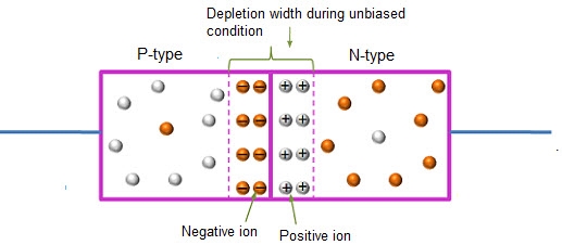
Figure 14: Unbiased or zero biased PN Junction Diode
FORWARD BIAS
In the forward bias condition, the positive terminal of the battery is connected to the P-Type material and the negative terminal of the battery is connected to the N-type material. This connection is also called as giving positive voltage.
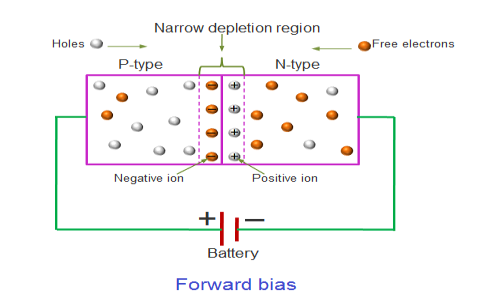
Figure 15: Forward bias
Electrons from the N-region cross the junction and enters the P-region. Due to the attractive force that is generated in the P-region the electrons are attracted and move towards the positive terminal. Simultaneously the holes are attracted to the negative terminal of the battery. By the movement of electrons and holes current flows. In this condition, the width of the depletion region decreases due to the reduction in the number of positive and negative ions.
If this external voltage Vf becomes greater than the value of the potential barrier, 1pprox.. 0.7 volts for silicon and 0.3 volts for germanium, the potential barriers opposition will be overcome and current will start to flow.
This is because the negative voltage pushes or repels electrons towards the junction giving them the energy to cross over and combine with the holes being pushed in the opposite direction towards the junction by the positive voltage. This results in a characteristics curve of zero current flowing up to this voltage point, called the “knee” on the static curves and then a high current flow through the diode with little increase in the external voltage as shown in I-V characteristics.
REVERSE BIAS
In the reverse bias condition, the negative terminal of the battery is connected to the P-type material and the positive terminal of the battery is connected to the N-type material. This connection is also known as giving negative voltage.
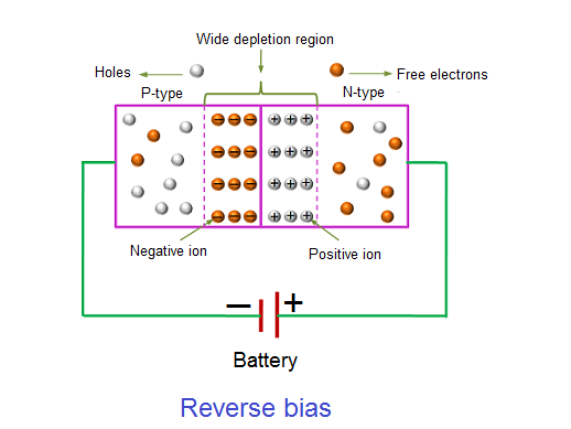
Figure 16: Reverse bias
The positive voltage applied to the N-type material attracts electrons towards the positive electrode and away from the junction, while the holes in the P-type end are also attracted away from the junction towards the negative electrode.
The net result is that the depletion layer grows wider due to a lack of electrons and holes and presents a high impedance path, almost an insulator. The result is that a high potential barrier is created thus preventing current from flowing through the semiconductor material.
This condition represents a high resistance value to the PN junction and practically zero current flows through the junction diode with an increase in bias voltage. However, a very small leakage current does flow through the junction which can be measured in micro-amperes, ( μA ).
If the reverse bias voltage Vr applied to the diode is increased to a sufficiently high enough value, it will cause the diode’s PN junction to overheat and fail due to the avalanche effect around the junction. This may cause the diode to become shorted and will result in the flow of maximum circuit current, and this shown as a step downward slope in the reverse static characteristics curve in I-V characteristics.
I-V CHARACTERISTICS OF PN JUNCTION DIODE
The I-V Characteristic Curves, which is short for Current-Voltage Characteristic Curves or simply I-V curves of an electrical device
The application of a forward biasing voltage on the junction diode results in the depletion layer becoming very thin and narrow which represents a low impedance path through the junction thereby allowing high currents to flow. The point at which this sudden increase in current takes place is represented on the static I-V characteristics curve above as the “knee” point. The current starts increasing with increase in voltage. At knee voltage current shows a sharp increment in its magnitude. This behaviour is mentioned above. As large current flow in forward biasing so we measure this current in mA.
When a junction diode is Reverse Biased, the thickness of the depletion region increases and the diode acts like an open circuit blocking current flow. So only a very small leakage current will flow.
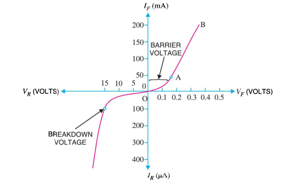
Figure 17: I-V characteristics
Key Takeaways
- A P-N Junction Diode is formed by doping one side of a piece of silicon with a P-type dopant (Boron) and the other side with a N-type dopant (phosphorus). Ge can be used instead of Silicon.
- Zero biased condition is the case when no external voltage is applied to the P-N junction diode.
- In the forward bias condition, the positive terminal of the battery is connected to the P-Type material and the negative terminal of the battery is connected to the N-type material. This connection is also called as giving positive voltage.
- In the reverse bias condition, the negative terminal of the battery is connected to the P-type material and the positive terminal of the battery is connected to the N-type material. This connection is also known as giving negative voltage.
The satisfactory explanation of this breakdown of the junction was first given by the American scientist C. Zener. A zener diode is a special type of diode that is designed to operate in the reverse breakdown region.
An ordinary diode operated in this region will usually be destroyed due to excessive current. This is not the case for the zener diode.
It has already been discussed that when the reverse bias on a crystal diode is increased, a critical voltage, called breakdown voltage is reached where the reverse current increases sharply to a high value. The breakdown region is the knee of the reverse characteristic as shown in Figure 19.
The breakdown voltage is sometimes called zener voltage and the sudden increase in current is known as zener current.
The breakdown or zener voltage depends upon the amount of doping. If the diode is heavily doped, depletion layer will be thin and consequently the breakdown of the junction will occur at a lower reverse voltage.
On the other hand, a lightly doped diode has a higher breakdown voltage. When an ordinary crystal diode is properly doped so that it has a sharp breakdown voltage, it is called a zener diode. A properly doped crystal diode which has a sharp breakdown voltage is known as a zener diode.
Figure 18 shows the symbol of a zener diode. It may be seen that it is just like an ordinal, diode except that the bar is turned into z-shape.
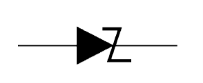
Figure 18: Symbol of a zener diode
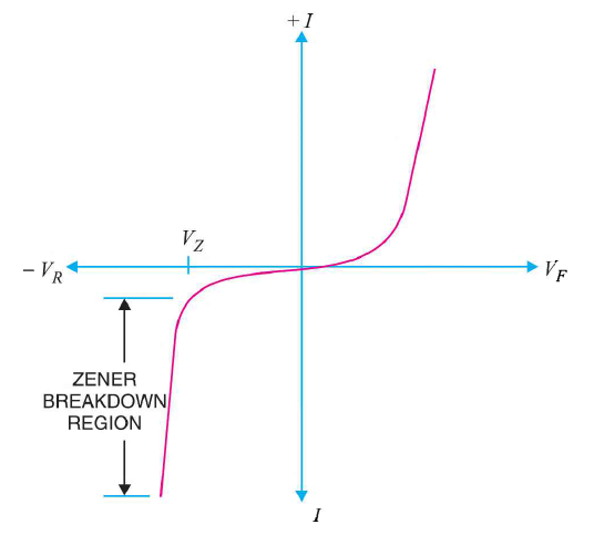
Figure 19: I-V characteristics of zener diode
As the curve reveals, two things happen when Vz is reached:
- The diode current increases rapidly.
- The reverse voltage Vz across the diode remains almost constant.
The following points may be noted
(i) A zener diode is like an ordinary diode except that it is properly doped so as to have a sharp breakdown voltage.
(ii) A zener diode is always reverse connected i.e. it is always reverse biased.
(iii) A zener diode has sharp breakdown voltage, called zener voltage Vz.
(iv) When forward biased, its characteristics are just those of ordinary PN junction diode.
(v) The zener diode is not immediately burnt just because it has entered the breakdown region. As long as the external circuit connected to the diode limits the diode current to less than burn out value, the diode will not burn out.
In other words, the zener diode operated in this region will have a relatively constant voltage across it, regardless of the value of current through the device. This permits the zener diode to be used as a voltage regulator or voltage stabiliser.
Key Takeaways
- A zener diode is a special type of diode that is designed to operate in the reverse breakdown region.
- The breakdown region is the knee of the reverse characteristic
- The breakdown voltage is sometimes called zener voltage and the sudden increase in current is known as zener current.
- The breakdown or zener voltage depends upon the amount of doping.
- Because of its special characteristics zener diode used as voltage stabiliser
Bipolar junction transistor or BJT is simply known as Transistor. A transistor consists of two pn junctions formed by sandwiching either p-type or n-type semiconductor between a pair of opposite types.
The prefix 'trans' means the signal transfer property of the device while 'istor ' classifies it as a solid element in the same general family with resistors.
Accordingly there are two types of transistors
- n-p-n transistor
- p-n-p transistor
An n-p-n transistor is composed of two n-type semiconductors separated by a thin section of p-type as shown in Figure 20 (i).
However, a p-n-p transistor is formed by two p-sections separated by a thin section of n-type as shown in Figure 20(ii).

Figure 20 (i) n-p-n transistor (ii) p-n-p transistor
In each type of transistor, the following points may be noted:
(i) Transistor may be regarded as a combination of two diodes connected back to back.
(ii) There are three terminals, one taken from each type of semiconductor.
(iii) The middle section is a very thin layer. The thin layer plays an important role in the function of a transistor.
A transistor has two pn junctions. One junction is forward biased and the other is reverse biased. The forward biased junction has a low resistance path whereas a reverse biased junction has a high resistance path. The weak signal is introduced in the low resistance circuit and output is taken from the high resistance circuit. Therefore, a transistor transfers a signal from a low resistance to high resistance.
A transistor (pnp or npn) has three sections of doped semiconductors. The section on one side is the emitter and the section on the opposite side is the collector. The middle section is called the base and forms two junctions between the emitter and collector.
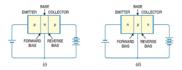
Figure 21 (i) p-n-p transistor (ii) n-p-n transistor
Emitter: The section on one side that supplies charge carriers (electrons or holes) is called the emitter. The emitter is always forward biased w.r.t. Base so that it can supply a large number of majority carriers. In Figure 21 (i), the emitter (p-type) of pnp transistor is forward biased and supplies hole charges to its junction with the base. Similarly, in Figure 21 (ii), the emitter (n-type) of npn transistor has a forward bias and supplies free electrons to its junction with the base.
Collector: The section on the other side that collects the charges is called the collector. The collector is always reverse biased. Its function is to remove charges from its junction with the base. In Figure 21 (i), the collector (p-type) of pnp transistor has a reverse bias and receives hole charges that flow in the output circuit. Similarly, In Figure 21 (ii), the collector (n-type) of npn transistor has reverse bias and receives electrons.
Base: The middle section which forms two pn junctions between the emitter and collector is called the base. The base emitter junction is forward biased allowing low resistance for the emitter circuit. The base-collector junction is reverse biased and provides high resistance in the collector circuit.
Before studying action of transistor, some important facts about transistor should be keep in mind.
- The transistor has two pn junctions i.e. it is like two diodes. The junction between emitter and base may be called emitter-base diode or simply the emitter diode. The junction between the base and collector may be called collector-base diode or simply collector diode.
- The emitter diode is always forward biased whereas collector diode is always reverse biased.
- Three regions of transistor are emitter, base and collector. The base is much thin as compared to emitter while "collector is wider than both. To keep it simple it is assumed emitter and collector is considered to be of same size.
- The emitter is heavily doped so that it can inject a large number of charge carriers (electrons or holes) into the base. The base is lightly doped and very thin it passes most of the emitter injected charge carriers to the collector. The collector is moderately doped.
- The resistance of emitter diode (forward biased) is very small as compared to collector diode (reverse biased). Therefore, forward bias applied to the emitter diode is generally very small whereas reverse bias on the collector diode is much higher.
Working of Transistor
(i) Working of npn transistor: As discussed in the npn transistor emitter-base junction is forward biased to emitter-base junction and collector-base junction is reverse biased. The forward bias causes the electrons in the n-type emitter to flow towards the base. This constitutes the emitter current Ie.
Ie = Ib + Ic
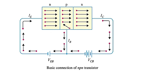
Figure 22: n-p-n transistor
As these electrons flow through the p-type base, they tend to combine with holes. As the base is lightly doped and very thin, therefore, only a few electrons (less than 5%) combine with holes to constitute base current Ib. The remainder i.e. more than 95% cross over into the collector region to constitute collector current Ic In this way, almost the entire emitter current flows in the collector circuit. It is clear that emitter current is the sum of collector and base currents i.e.
(ii) Working of pnp transistor: In the pnp transistor emitter-base junction is forward biased to emitter-base junction and collector-base junction is reverse biased. The forward bias causes the holes in the p-type emitter to flow towards the base. This constitutes the emitter current Ie. As these holes cross into n-type base, they tend to combine with the electrons. As the base is lightly doped and very thin, therefore, only a few holes (less than 5%) combine with the electrons.
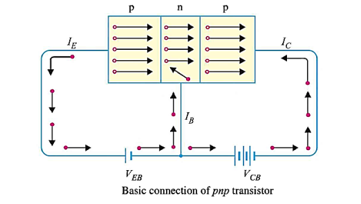
Figure 23: p-n-p transistor
The remainder (more than 95%) cross into the collector region to constitute collector current Ic. In this way, almost the entire emitter current flows in the collector circuit. It may be noted that current conduction within pnp transistor is by holes. However, in the external connecting wires the current is still by electrons.
Thus the input circuit (i.e. emitter-base junction) has low resistance because of forward bias whereas output circuit (i.e. collector base junction) has high resistance due to reverse bias. As we have seen, the input emitter current almost entirely flows in the collector circuit. Therefore a transistor transfers the input signal current from a low resistance circuit to a high-resistance circuit.
Key Takeaways
- A transistor consists of two pn junctions formed by sandwiching either p-type or n-type semiconductor between a pair of opposite types.
- There are two types of transistors n-p-n transistor and p-n-p transistor.
- The emitter diode is always forward biased whereas collector diode is always reverse biased.
- Three regions of transistor are emitter, base and collector. The base is much thin as compared to emitter while "collector is wider than both. To keep it simple it is assumed emitter and collector is considered to be of same size.
- The emitter is heavily doped so that it can inject a large number of charge carriers (electrons or holes) into the base. The base is lightly doped and very thin it passes most of the emitter injected charge carriers to the collector. The collector is moderately doped.
Reference Books
- Principle of electronics S. Chand V K Mehta and Rohit Mehta
- A textbook of Engineering Physics, Dr. M. N. Avadhanulu, Dr. P.G. Kshirsagar - S.Chand
- J. Singh, Semiconductor Optoelectronics: Physics and Technology, Mc Graw-Hill inc.(1995).