UNIT 3
OPTOELECTRONICS
Recombination mechanisms can in general be classified into two groups, radiative and nonradiative.
Radiative recombination
Radiative recombination occurs when an electron in the conduction band recombines with a hole in the valence band and the excess energy is emitted in the form of a photon.
Radiative recombination is thus the radiative transition of an electron in the conduction band to an empty state (hole) in the valence band.
In semiconductors electrons can make transitions between two energy states and generate or destroy photons in the process. In particular, transitions between the conduction band (EC) and the valence band ( EV) are optically active. As the lower conduction band generally consists of s-like states while the upper valence band contains of p-like states. Spontaneous emission, absorption, and stimulated emission can all take place between conduction band (EC) states and valence band (EV) states.
The optical processes associated with radiative transitions are
(i) spontaneous emission, (ii) absorption or gain, and (iii) stimulated emission.
Absorption
- Similar to stimulated absorption in optics in the semiconductor absorption all we need is an incoming photon, a valence band energy state occupied by an electron, and an empty conduction band energy state.
- We know that in equilibrium condition, the valence band is fully occupied and the conduction band is empty.
- We know that for optical absorption between two states in an atom only occurred for a narrow spectrum of photon energies so here in optical absorption in a semiconductor can occur over a wide range of photon energies.
- This process carry out when the energy photon is greater than or equal to the band gap energy.
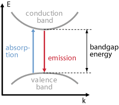
Figure 1: Band gap energy diagram
- Incoming photon interacts with electron in valence band and provides it sufficient energy for excitation and by getting enough energy the electron jump to conduction band and leaving hole in valence band.
- The absorption process creates an electron in the conduction band and a hole in the valence band, it is also called optical generation.
- If the electrons created at energies higher than the band edge will quickly stabilize to the lowest conduction band energy states by releasing phonons.
- Holes created deep in the valence band will ‘float up’ to the valence band edge.
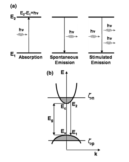
Figure 2: Absorption or gain, spontaneous emission and stimulated emission.
Spontaneous Emission
- Consider the system is in equilibrium but temperature is increased let us consider it is at T temperature.
- Electrons and holes can be created by optical absorption and other pumping mechanisms.
- The spontaneous emission process is possible for a wide range of photon energies above the band gap similar to absorption.
- At T temperature the lowest energy states are mostly full in conduction band.
- At T temperature the highest energy states are mostly empty in valence band.
- Therefore, the spontaneous emission observed in semiconductor in which photon has energy nearly equal to the band gap energy.
- Since the spontaneous emission process ‘destroys’ an electron and a hole, it is also called spontaneous optical recombination.
Stimulated emission
- The stimulated emission process ‘destroys’ an electron and a hole, it is also called stimulated optical recombination.
- In order to make stimulated emission the dominant optical process, we need to achieve population inversion.
- It is the most important process for laser operation.
- In this process a copy of the incoming photon is produced.
- We expect that in most cases the stimulated emission will occur primarily between band-edge states, as these states are most likely to be occupied with electrons and holes just like in spontaneous emission.
- Semiconductor optical amplifiers generally amplify light whose photon energy is approximately equal to the band gap energy of the semiconductor gain medium.
In thermal equilibrium, a direct-band-gap semiconductor (e.g., GaAs, InP, or GaSb) has a few electrons in the conduction band and a few holes (empty electron states) in the valence band. When a photon of energy greater than the band gap passes through such a semiconductor, the photon has a high probability of being absorbed, giving its energy to an electron in the valence band, thereby raising the electron to the conduction band. In principle, such a photon could stimulate the emission of an identical photon with the transition of an electron from the conduction to the valence band. The emitted photon derives its energy from the energy lost by the electron.
In thermal equilibrium the number of electrons in the conduction band is very small, so the probability of stimulated emission is negligible compared to the probability for absorption. However, external excitation, can sufficiently increase the number of electrons in the conduction band such that the probability of stimulated emission eventually becomes higher than the probability of absorption. This situation corresponds to population inversion in a laser medium and is necessary for optical gain.
The external excitation which generates a high density of electron-hole pairs in a semi-conductor is usually provided by current injection. It can also be achieved by optical pumping (absorption of radiation higher in energy than the band gap).
1 Radiative electron-hole recombination: Under the equilibrium then the law of mass action states that the product of electron and hole concentration, under a given temperature, is constant
n0p0 =  …………..(1)
n0 - equilibrium electron concentration
p0 - equilibrium hole concentration
ni -intrinsic carrier concentration
Total carrier concentration is given by sum of equilibrium and excess carrier concentration
n=n0+ ∆n and p=p0+ ∆p …………..(2)
The recombination rate is proportional to the product to the electron and hole concentration, that is
R ∝ np.
The recombination rate per unit time per unit volume can then be written
R =  −=
−=  − = Bnp …………..(3)
This is the bimolecular rate equation, and B is a constant called bimolecular recombination coefficient, where the typical value is 10−11-10−9cm3/s for III-V semiconductors.
2 Radiative recombination for low-level exciton: Electrons and holes are generated and anhilated (by recombination) in pairs, the steady state hole and electron excess concentration are equal,
i.e. ∆n(t)=∆p(t),
And from equation (3) we will get
 …………..(4)
For the case of low-level excitation, the photo-generated carrier concentration is much smaller than majority carrier concentration, ∆n<<(n0+p0), and we also have that ∆n(t)=∆p(t) we will then get from equation (4)
 …………..(5)
The time dependent carrier concentration calculated from the rate equation is
 …………..(6)
Semiconductor has been illuminated with the light and excess carriers are generated, G0=R0
 …………..(7)
And the solution will be
 …………..(8)
And after rewriting we get
 …………..(9)
Where τ is the carrier lifetime

In the case for low-level excitation the photo generated carrier concentration is much smaller than the majority carrier concentration. However the photogenerated carrier concentration is much larger than the minority carrier concentration.
3 Radiative recombination for high-level excitation: For high-level excitation, the photogenerated carrier concentration is larger than equilibrium carrier concentration, i.e. ∆n>> (n0+p0). Bimolecular rate equation is then given by
 …………..(10)
And then we get
 …………..(11)
The time constant here will be
 …………..(12)
Minority carrier lifetime increases with time. For sufficiently long times, low-level excitation conditions will be reached and τ will approach the low-level value.
Nonradiative Recombination
In indirect-band-gap semiconductors such as Ge or Si, the probability of nonradiative recombination dominates that of radiative recombination by several orders of magnitude. The measurable quantities associated with nonradiative recombination are the internal quantum efficiency and the carrier lifetime. The variation of these quantities with parameters like temperature, pressure and carrier concentration is, by and large, the only way to identify a particular nonradiative recombination process. One of the effects of nonradiative recombination on the performance of injection lasers is to increase the threshold current.
The nonradiative recombination processes that affect the performance of long-wavelength semiconductor lasers are Auger recombination, surface recombination, and recombination at defects. The Auger recombination mechanism involves four particle states (three electrons and one hole) and is believed to be important at high temperatures and for low band-gap semiconductors.
Nonradiative recombination of an electron-hole pair, as the name implies, is characterized by the absence of an emitted photon in the recombination process.
During the non-radiative recombination, the electron energy is converted to vibrational energy of lattice atoms, i.e. phonons. Thus the electron energy is converted to heat. Most common cause for non-radiative recombination events are defects in the crystal structure.
This effects include unwanted foreign atoms, native defects, dislocations. All such defects have energy level structure that is different from substantial semiconductor atoms. And it’s quite common for such defects to form one or several energy levels within the forbidden gap of the semiconductor.
Energy levels within the gap of the semiconductors are efficient recombination centers, in particular if the energy level is close to the middle of the gap.
Trap-assisted recombination occurs when an electron falls into a ”trap”, this is an energy level within the bandgap caused by the presence of a foreign atom or a structural defect. Once the trap is filled it cannot accept another electron. The electron occupying the trap, in a second step, falls into an empty valence band state, thereby completing the recombination process. The non-radiative recombination rate through a deep level with trap energy ET and concentration NT
 …………..(13)
∆n=∆p
vn and vp = electron and hole velocities
σn and σp= capture cross section of the traps
n1 and p1= electron and hole concentrations if the Fermi energy is located at the trap levels:
 …………..(14)
EFi- Fermi level in the intrinsic semiconductors.Non radiative lifetime of excess electrons can be deduced from RSR= ∆n/τ, which will give
 …………..(15)
If we assume p-type semiconductor, i.e. the holes are in majority p0>> n0 and p0 >> p1, and we assume small deviation from equilibrium, i.e. ∆n << p0 then minority carrier lifetime is given by
 …………..(16)
If the electrons were majority carriers, the lifetime would be
 …………..(17)
Results shows that Shcockley - Read recombination rate is limited by the rate of the capture of minority carriers, since the capture of majority carriers is much more likely event than the capture of minority carriers. From equation (15) we will get
 …………..(18)
For small deviations from equilibrium, i.e ∆n << p0, which will give
 …………..(19)
The lifetime does not change for small deviations from equilibrium in an extrinsic semiconductor. We assume that the trap captures electrons and holes at the same rate, i.e. vnσn=vpσpandτn0=τp0, and we get from equation (19)
 …………..(20)
For special case of intrinsic material, i.e.n0= p0= ni the equation becomes
 …………..(21)
EFi - the Fermi level typical close to the middle of gap.
The non-radiative life time is minimized, if ET - EFi is zero, when the trap level is at or close to the mid gap energy. For such mid gap levels the lifetime is given by τ=2τn0 This shows that deep levels are effective recombination centers if they are near in the middle of the gap.
Auger recombination
Another non-radiative recombination is Auger recombination, it is given off in the form of kinetic energy to another electron. The energy that becomes available through electron-hole recombination (Eg) is dissipated by the excitation of a free electron high into the conduction band, or by a hole deeply excited into the valence band. The highly excited carrier will subsequently lose energy by multiple phonon emission until they are close to the band edge. Recombination rate due to the Auger process
RAuger = Cpnp2 (22)
RAuger = Cnn2p (23)
Auger recombination reduces the luminescence efficiency in semiconductors only at very high excitation intensity or at very high carrier injection currents. At lower carrier concentrations, the Auger recombination rate is very small and can be neglected.
Auger recombination involves three particles: an electron and a hole, which recombine in a band-to-band transition and give off the resulting energy to another electron or hole. The expression for the net recombination rate is therefore similar to that of band-to-band recombination but includes the density of the electrons or holes, which receive the released energy from the electron-hole annihilation.
In other words Auger recombination the energy is given to a third carrier which is excited to a higher energy level without moving to another energy band.
After the interaction, the third carrier normally loses its excess energy to thermal vibrations. Since this process is a three-particle interaction, it is normally only significant in non-equilibrium conditions when the carrier density is very high.
Auger recombination is most important at high carrier concentrations caused by heavy doping. In silicon-based solar cells, Auger recombination limits the lifetime and ultimate efficiency.
The more heavily doped the material is, the shorter the Auger recombination lifetime.
Non-radiative recombination at surfaces
Recombination at surfaces and interfaces can have a significant impact on the behavior of semiconductor devices.
Just as for surface recombination, non-radiative bulk recombination and Auger recombination can never be totally avoided. Any semiconductor crystal will have some native defects. It is also difficult to fabricate materials with impurity levels lower than the parts per billion range (ppb). Thus even the purest semiconductors contain impurities in the 1012cm−3.The total probability of recombination is given by the sum of the radiative and non-radiative probabilities
τ−1 =  +
+  ………….(24)
Where τr and τnr are radiative and non-radiative lifetime.
The relative probability of radiative recombination is given by radiative probability over the total probability of recombination. Thus the probability of radiative recombination or internal quantum efficiency is given by  …….….. (25)
The internal quantum efficiency gives the ratio of the number of light quanta emitted inside the semiconductor to the number of charge quanta undergoing recombination. Not all photons emitted internally may escape from the semiconductor due to the light escape problem, reabsorption in the substrate, or after reabsorption mechanism.
Areas of defect, such as at the surface of solar cells where the lattice is disordered, recombination is very high.
This is because surfaces and interfaces typically contain a large number of recombination centers because of the abrupt termination of the semiconductor crystal, which leaves a large number of electrically active states.
In addition, the surfaces and interfaces are more likely to contain impurities since they are exposed during the device fabrication process.
The net recombination rate due to trap-assisted recombination and generation is given by:

The recombination is due to a two-dimensional density of traps, Nts, as the traps only exist at the surface or interface.
Understanding the impacts and the ways to limit surface recombination leads to better and more robust solar cell designs. Surface recombination is high in solar cells, but can be limited.
Atoms at the surface cannot have the same bonding structure as bulks atoms due to the lack of neighbouring atoms. Thus some of the valence orbitals do not form a chemical bond. These partially filled electron orbitals, or dangling bonds, are electronic states that can be located in the forbidden gap of the semiconductor where they act as recombination center.
Surface recombination leads to a reduced luminescence efficiency and also to a heating of the surface due to non-radiative recombination at the surface. Both effects are unwanted in electroluminescent devices.
Surface recombination can occur only when both type of carrier are present. It is important in the design of LEDs that the carrier-injected active region, in which both type of carriers are presented, be far removed from any surface. This can be archived by carrier injection under a contact that is much smaller than the semiconductor die
Key Takeaways
- Recombination mechanisms can in general be classified into two groups, radiative and nonradiative.
- Radiative recombination occurs when an electron in the conduction band recombines with a hole in the valence band and the excess energy is emitted in the form of a photon.
- The optical processes associated with radiative transitions are (i) spontaneous emission, (ii) absorption or gain, and (iii) stimulated emission.
- The recombination rate per unit time per unit volume can then be written R =
 −=
−=  − = Bnp. This is the bimolecular rate equation, and B is a constant called bimolecular recombination coefficient.
 - In case of Radiative recombination for low-level exciton the carrier lifetime τ is given by

- For high-level excitation, The time constant will be

- Nonradiative recombination of an electron-hole pair, as the name implies, is characterized by the absence of an emitted photon in the recombination process.
- Auger and surface recombination are Non radiative recombination.
LED or Light emitting diode
Light emitting diode is a pn junction device. It is always operated in forward biased condition. LED converts electrical energy into light energy.
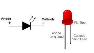
Figure 3: LED
Device Structure:
The LED structure plays a crucial role in emitting light from the LED surface. The LEDs are structured to ensure most of the recombination takes place on the surface by the following two ways.
- By increasing the doping concentration of the substrate, so that additional free minority charge carriers electrons move to the top, recombine and emit light at the surface.
- By increasing the diffusion length L =√Dτ, where D is the diffusion coefficient and τ is the carrier life time.
But when increased beyond a critical length there is a chance of reabsorption of the photons into the device. The LED has to be structured so that the photons generated from the device are emitted without being reabsorbed.
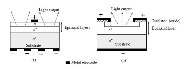 Figure 4: A schematic illustration of typical planar surface emitting LED devices. (a) p-layer grown epitaxially on an n+ substrate. (b) First n+ is epitaxially grown and then p region is formed by dopant diffusion into the epitaxial layer.
One solution is to make the p layer on the top thin, enough to create a depletion layer. Following picture shows the layered structure. There are different ways to structure the dome for efficient emitting
LEDs are usually built on an n-type substrate, with an electrode attached to the p-type layer deposited on its surface. P-type substrates, while less common, occur as well. Many commercial LEDs, especially GaN/InGaN, also use sapphire substrate.
In the fabrication of LED’s direct band gap semiconductors like GaP, GaAsP are used. In direct band gap semiconductors most of the energy is emitted in the form of light when hole and electron recombination takes place.
When an LED is forward biased the electrons and holes move in towards the junction and recombination takes place. As a result of recombination the electrons lying in the conduction band of an n- region fall into the holes lying in the valence band of a p –region. The difference of energy in the valence band and conduction band is radiated in the form of light energy. Here their excess energy is transferred to the emitted photon. The brightness of emitted light is directly proportional to the forward bias current.
Figures of Merit
A very important metric of an LED is the external quantum efficiency ηext. It quantifies the efficiency of the conversion of electrical energy into emitted optical energy.
Not all the photons emitted from the active region of an LED make it out of the device. Some are reabsorbed, some go in the wrong direction, some are reflected back. The light extraction efficiency of a LED is,
ηextraction 
The external quantum efficiency ext of a LED is,
ηextraction 
It is defined as the light output divided by the electrical input power. It is also defined as the product of Internal radiative efficiency and Extraction efficiency. ηext = Pout(optical) / IV
For indirect bandgap semiconductors ηext is generally less than 1%, whereas for a direct band gap material it could be substantial.
ηint = rate of radiation recombination/ Total recombination
The internal efficiency is a function of the quality of the material and the structure and composition of the layer.
LED materials
LEDs are comprised of compound semiconductor materials, which are made up of elements from group III and group V of the periodic table (these are known as III-V materials). Examples of III-V materials commonly used to make LEDs are gallium arsenide (GaAs) and gallium phosphide (GaP).
Ternary alloys based on alloying GaAs and GaP which are denoted by GaAs1-yPy. InGaAlP is an example of a quarternary (four elements) III-V alloy with a direct band gap. The LEDs realized using two differently doped semiconductors that are the same material is called a homojunction. When they are realized using different bandgap materials they are called a heterostructure device. A heterostructure LED is brighter than a homoJunction LED.
The main semiconductor materials used to manufacture LEDs are:
- Indium gallium nitride (InGaN): blue, green and ultraviolet high-brightness LEDs
- Aluminum gallium indium phosphide (AlGaInP): yellow, orange and red high-brightness LEDs
- Aluminum gallium arsenide (AlGaAs): red and infrared LEDs
- Gallium phosphide (GaP): yellow and green LEDs
Characteristics of LED
LEDs are solid-state devices. The advantages are:
1) Light Generated by LED is Directional
2) LED can Generate Different Light Color
3) Temperature will Affect LED Efficacy
4) Low Energy Consumption
5) Long Life
The usage of LED is advantageous as it consumes less power and produces less heat. LEDs last longer than incandescent lamps.
Applications LEDs are used in
- For instrument display
- In calculators
- Digital clocks
- For indicating power ON/ OFF
- For optical switching application
- In optical communication system
- Medical devices
Key Takeaways
- Light emitting diode is a pn junction device. It is always operated in forward biased condition. LED converts electrical energy into light energy.
- When an LED is forward biased the electrons and holes move in towards the junction and recombination takes place.
- The light extraction efficiency of a LED is,
ηextraction 
- LEDs are comprised of compound semiconductor materials, which are made up of elements from group III and group V of the periodic table (these are known as III-V materials). Examples of III-V materials commonly used to make LEDs are gallium arsenide (GaAs) and gallium phosphide (GaP).
SEMICONDUCTOR LASERS: DEVICE STRUCTURE, MATERIALS, CHARACTERISTICS AND FIGURES OF MERIT
It is a solid state semiconductor laser. It is specifically fabricated p-n junction diode. This diode emits laser light when it is forward biased. A semiconductor laser is a device that causes laser oscillation by flowing an electric current to semiconductor. The mechanism of light emission is the same as a light-emitting diode (LED). Light is generated by flowing the forward current to a p-n junction. In forward bias operation, the p-type layer is connected with the positive terminal and the n-type layer is connected with the negative terminal, electrons enter from the n-type layer and holes from the p-type layer. When the two meet at the junction, an electron drops into a hole and light is emitted at the time.
We know that Laser radiation is highly monochromatic and it produces highly directional beams of light. In similar manner Semiconductor lasers works just like any other solid-state lasers and gas laser. The emitted radiation has spatial and temporal coherence. In spite of this similarity semiconductor lasers differ from other lasers in several important respects:
- In case of conventional lasers, the quantum transitions occur between discrete energy levels, whereas in case of semiconductor lasers the transitions are associated with the band properties of materials.
- Size of semiconductor laser is very compact almost of the order of 0.1mm long this is because the active region is very narrow of the order of 1μm thick or less, the divergence of the semiconductor laser beam is considerably larger than in case of conventional laser.
- The spatial and spectral characteristics of a semiconductor laser are strongly influenced by the properties of the junction medium (such as band gap and refractive index variations).
- For the p-n junction laser, the laser action is produced by simply passing a forward current through the diode itself. The result is a very efficient overall system that can be modulated easily by modulating the current. Since semiconductor lasers have very short photon lifetimes, modulation at high frequencies can be achieved.
Semiconductor laser is one of the most important light sources for optical-fiber communication because of its compact size and capability for high-frequency modulation.
Semiconductor Materials
All the lasing semiconductors have direct bandgaps. This is expected since the radiative transition in a direct bandgap semiconductor is a first-order process. Which implies that the momentum is automatically conserved. The transition probability is high.
For indirect bandgap semiconductors, the radiative transition is a second-order process that simply means it involves phonons or other scattering agents to conserve momentum and energy. Thus the radiative transition is much weaker.
Figure shows the range of laser emission wavelengths for various semiconductors from near ultraviolet to far infrared.
GaAs was the first material to lase, and its related III—V solid solutions have been most extensively studied and developed.
The IV—VI compounds, such as PbS, PbTe, PbSe, and related solid solutions, also exhibit laser action. They are direct bandgap materials with their extrema located along the (1 1 1) directions in the Brillouin zone, in contrast to GaAs with extrema located at the zone center.
In this section, we consider basic laser physics and use examples mainly from devices of III—V compound semiconductors. When compound semiconductors are formed that have more than one group III element distributed randomly on group III lattice sites or more than one group V element distributed randomly on group V lattice sites, these compounds are crystalline solid solutions.
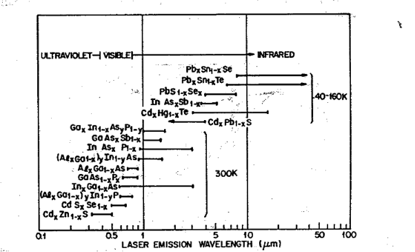
Figure 5: shows the range of laser emission wavelengths for various
The notation frequently used is AxB1-xCy for ternary and AxB1-xCyD1-y for quaternary compounds, where A
And B are the group III elements and C and D are the group V elements.
The two most important Ill—V compound systems are AIxGa1-xAsySb1-y and GaxIn1-xAsyP1-y, solid solutions.
To achieve hetero structures with negligible interface traps, the lattices between the two semiconductors must be closely matched. The list of semiconductor materials that have exhibited laser action has continued to grow.
Semiconductor lasers require, for the active medium, a direct gap material and accordingly, the normal elemental semiconductors like Si or Ge cannot be used. The majority of semiconductor-laser materials are based on a combination of elements belonging to the third group of the periodic table such as Al, Ga, In with elements of the fifth group such as N, P,As, Sb. Examples include the best known GaAs as well as some ternary AlGaAs, InGaAs and quaternary InGaAsP alloys.
InGaN semiconductor lasers the best candidates for semiconductor laser emission in the very important blue-green spectral region. Semiconductor laser materials are not limited to III–V compounds, however. For the blue-green end of the spectrum we note that there are wide-gap semiconductors using a combination between elements of the second group (such as Cd and Zn) and of the sixth group (S, Se).
Double Heterostructure Laser
Figure 6 shows the basic structure of a p-n junction laser. Pair of parallel planes are cleaved or polished perpendicular to the plane of the junction. The two remaining sides of the diode are roughened to eliminate lasing in directions other than the main one. The structure is called a Fabry-Perot cavity.
When a forward bias is applied to the laser diode, a current flows. Initially at low current, there is spontaneous emission in all directions. As the bias is increased, eventually a threshold current is reached at which the stimulated emission occurs and a monochromatic and highly directional beam of light is emitted from the junction (Figure 6).
For the homostructure (e.g., GaAs p-n junction), the threshold current density increases rapidly with increasing temperature. A typical value of Jth (obtained by pulse measurement) is about 5.0 x 10⁴ A/cm2 at room temperature. Such a large current density imposes serious difficulties in operating the laser continuously at 300K. To reduce the threshold current density, heterostructure lasers have been proposed and built using epitaxial technique.
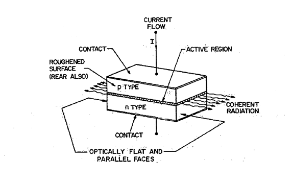
Figure 6: Structure of junction laser in the form of Fabry Perot Cavity
Semiconductor lasers represent one of the most important class of lasers in use today, not only because of the large variety of direct applications in which they are involved but also because they have found a widespread use as pumps for solid state lasers.
Key Takeaways
- It is a solid state semiconductor laser. It is specifically fabricated p-n junction diode. This diode emits laser light when it is forward biased. A semiconductor laser is a device that causes laser oscillation by flowing an electric current to semiconductor. The mechanism of light emission is the same as a light-emitting
- The two most important Ill—V compound systems are AIxGa1-xAsySb1-y and GaxIn1-xAsyP1-y, solid solutions.
- The basic structure of a p-n junction laser.is called a Fabry-Perot cavity.
- For the homostructure (e.g., GaAs p-n junction), the threshold current density increases rapidly with increasing temperature
Solar Cells
A solar cell or photo-voltaic cell is an electronic device that directly converts sun’s energy into electricity. When sunlight falls on a solar cell, it produces both a current and a voltage to produce electric power.
Sunlight, which is composed of photons, radiates from the sun. When photons hit the silicon atoms of the solar cell, they transfer their energy to lose electrons; and then, these high-energy electron flow to an external circuit.
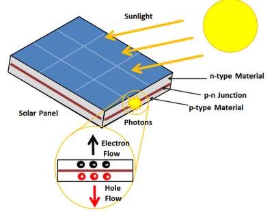
Figure 7: Solar Cell
The solar cell is composed of two layers which are struck together. The first layer is loaded with electrons, so these electrons are ready to jump from the first layer to the second layer. The second layer has some electrons taken away, and therefore, it is ready to take more electrons.
The advantages of solar cells are that, there is no fuel supply and cost problem. These are very dependable and require little maintenance.
A key issue with solar cells is conversion efficiency—convening the maximum amount of available solar energy into electrical energy. The higher the efficiency of the cells, the lower the cost and collection area required to achieve a desired electrical output.
A number of factors enter into the overall efficiency exhibited by a cell and involve both material and design considerations. Any discussion of conversion efficiency logically begins with the output from the sun.
Given a specific semiconductor material, it is the task to design and fabricate the solar cell to minimize further energy losses. In discussing device-related loss mechanisms, we will refer to the high-efficiency Si solar cell pictured in Figure 8.
Observe first of all that the contact to the top (light-incident) side of the cell is made through narrow "fingers." The fingers, all connected together along one edge of the cell are a design compromise. Zero-width fingers or fingers only along the cell edges would allow maximum light penetration to the underlying silicon. However, a series resistance of only a few ohms can seriously degrade the efficiency of a solar cell. The farther apart the fingers, the longer the current path through the narrow n-region at the top of the cell, and the greater the series resistance. Metallization and contact resistances can become important if the fingers are too narrow. The chosen finger size and spacing are calculated to provide an optimum trade-off between residual "shadowing," blocking of some of the light that strikes the cell, and cell series resistance.
Another potentially significant loss mechanism is the reflection of light at the Si surface. Approximately 30% of the light striking a bare planar Si surface at normal incidence will be reflected. To minimize losses due to reflection, the top surface of solar cells are typically "textured" and covered with an antireflection coating. Texturing of the surface, the formation of the inverted pyramids in decreases the reflected light by forcing the light to strike the Si surface two or more times before escaping.
Texturing is achieved by placing the Si in an anisotropic etching solution, an etch that preferentially removes Si atoms along certain crystalline planes. Having an index of refraction intermediate between air and Si, the top SiO2 layer in the pictured cell, or preferably a deposited antireflection coating with optimized parameters, further reduces the reflection.
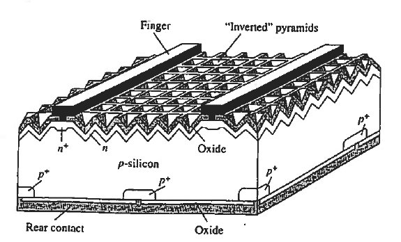
Figure 8: Solar Cell
Solar cells constructed in the described manner have attained a net reflection of less than 1%. Once the light has entered the semiconductor, the focus shifts to maximizing the light absorption.
In the Figure 8 solar cell the bottom surface oxide and metallization effectively form a mirror that reflects light hack into the silicon. Long wavelength light literally 1 bounces back and forth between the top and bottom surfaces of the cell. This "light trap-ping" dramatically enhances the long (λ— λG) wavelength absorption.
Finally, the cell must be designed and built to collect as many of the photogenerated minority carriers as possible. This necessitates minimizing carrier recombination through-out the device structure.
Very long minority carrier lifetimes are the rule in modern single-crystal Si cells, yielding diffusion lengths greater than the width of the cell. With the top and bottom surfaces also carefully oxidized to minimize surface recombination, carriers generated almost anywhere in the cell volume have a high probability of diffusing to the depletion region and being swept to the opposite side of the junction before they recombine.
Solar Cell Basics
A variety of device structures have been employed in constructing solar cells. By far and away the most common cells are in essence just large-area pn junction photodiodes. Solar cells are designed of course to minimize energy losses, whereas photodiodes arc routinely designed to achieve a specific spectral response or a rapid time response.
Although there is design differences but I—V characteristics of solar cell are of the same general form as the photodiode characteristics.
We know that power is derived from the illuminated device if the d.c. Operating point lies in the fourth quadrant where I is negative and V is positive. Fourth-quadrant operation can be achieved in case of solar cell just by simply placing a resistor in series with the illuminated solar cell.
The fourth-quadrant characteristic is of prime interest in evaluating and applying solar cells. It is therefore common practice to show only the fourth-quadrant portion of the characteristics and to orient the — I axis upward on the plot as illustrated in Figure 9.
Figure 9 also graphically defines the following solar cell parameters of interest:
Voc - the open circuit voltage
Isc - the short circuit current
Vm Im - the operating point voltage and current yielding the maximum power output.
Voc is obviously the maximum voltage that can be supplied by the cell for a given photoinput,
Is, is the maximum current that can be derived from the cell.
It follows that Pmax = Vm Im < Voc Isc
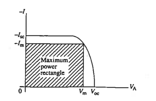
Figure 9: Inserted fourth-quadrant I—V characteristic of a solar cell under illumination with key solar cell parameters identified along the coordinate axes.
In calculations of solar cell performance, one often encounters

FF is known as the fill factor and is of course always less than unity.
The ultimate measure of solar cell performance, the power conversion efficiency (n), is determined from the current-voltage parameters employing

Where Pin, is the photo-energy incident per second or input power.
Key Takeaways
- A solar cell or photo-voltaic cell is an electronic device that directly converts sun’s energy into electricity.
- When sunlight falls on a solar cell, it produces both a current and a voltage to produce electric power.
- The advantages of solar cells are that, there is no fuel supply and cost problem. These are very dependable and require little maintenance.
- The higher the efficiency of the cells, the lower the cost and collection area required to achieve a desired electrical output.
- In calculations of solar cell performance, one often encounters fill factor FF is given by

P-I-N AND AVALANCHE
p-i-n Diode
In p-i-n diode an “intrinsic” (actually lightly doped) I region is sandwiched between heavily doped p- and n-regions. It is p-i-n diode is a three-region structure
In the p-i-n photodiode shown schematically in Figure 10. An opening is made in the surface metallization to admit light, the top semiconductor region is kept very thin no minimize absorption in the region and the i-layer width is specifically tailored so achieve the desired response characteristics. Because of the low doping the i-layer is totally depleted under zero bias or becomes depleted at small reverse biases.
Furthermore, the heavy doping of the outer p and n regions causes the depletion widths in these regions to be very narrow. Thus as pictured in a Figure 11
The depletion width inside the device is effectively equal to the i-layer width independent of the applied reverse bias. The energy bands (in Figure 11) are linear functions of position and the ξ-field is approximately constant in the i-region because of the low semiconductor doping.
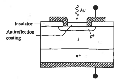
Figure 10: p-i-n photodiode Cross section.
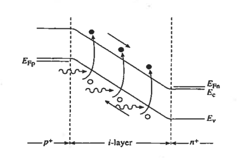
Figure 11: p-i-n photodiode Reverse bias energy band diagram.
It should also be noted than the heavy doping of the outer p and n regions causes the depletion means the minority carriers diffusion lengths in these regions will be relatively small. As a result, the greater part of the photocurrent flowing in a p-i-n photodiode arises from carriers generated in the central depletion region.
Operational advantages of the p-i-n photodiode that have made it one of the most widely employed photodetectors stem, from the existences and tailorability of the i-region.
For one, the diode con be optimized for response at a given wavelength by making the layer width equal to the inverse of the absorption coefficient (1/ ) of the specified wavelength Second, with one of the most photocurrent arising from light absorption to the i-region. Frequency response is greatly enhanced over that of a pn junction photodiode. The large ‘ξ-field is the depleted i-region leads to the rapid collection of photo generated carriers and a maximum frequency response.

Where WI is the width of the I region
Vsat is the saturation drift velocity
If WI = 5 then fmax =20GHz
The WI cannot be made arbitrary small to improve frequency.
The RC time constant associated with the internal series resistance (Rs)and the junction capacitance (CJ = Ks 0A/ WI) increases with decreasing WI and eventually limits the response time of the diode.
The excellent frequency response of the p-i-n photodiode makes it important for use as the photo detector in optical fiber telecommunication.
Avalanche Photodiode
Avalanche Photodiode are specially constructed p-i-n, pn, or even metal-semiconductor photodiodes that are operated near the avalanche breakdown point. A standard Si avalanche photodiode configuration is shown in figure.
One obvious special structural feature is the guard ring around the junction periphery. As noted in junction curvature leads to early breakdown about the junction periphery. The guard ring minimization of defect creation during device processing are also required to achieve uniform breakdown across the face of the junction. The primary advantage of the avalanche photodiode is a photo-signal gain leading to improvement in the signal-to-noise (S/N) ratio.
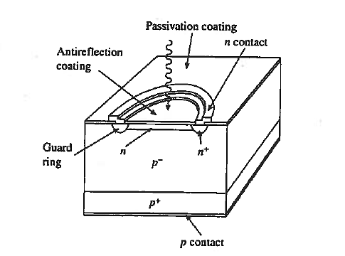
Figure 12: Avalanche Photodiode
As a general rule, amplification of signals is accompanied by amplification of the noise and added noise from the amplifier. Signal pain therefore typically loads to a reduction in the S/N ratio. Inside an avalanche photodiode, however, avalanche multiplication amplifies the photo-signal without amplifying the typically dominant receiver circuit noise. Thus there is an improvement in the S/N ratio until the added avalanche-related noise becomes comparable to the circuit noise.
Avalanche photodiodes made from lnGaAs on lnP and from Ge provide alternatives to the p-i-n photodiode for use in fiber optic telecommunication.
Key Takeaways
- In p-i-n diode an “intrinsic” (actually lightly doped) I region is sandwiched between heavily doped p- and n-regions. It is p-i-n diode is a three-region structure
- A maximum frequency response is given by

- Avalanche Photodiode are specially constructed p-i-n, pn, or even metal-semiconductor photodiodes that are operated near the avalanche breakdown point.
References
- Semiconductor Device Fundamentals by Robert F. Pierret
- Physics of Semiconductor Devices by S.M. Sze.
- Electronic and optoelectronic properties of Semiconductor Structures by Jasprit Singh.