Unit - 2
Semiconductors, Diode and Transistors
Atomic Theory
The smallest piece of an element is called an atom. An atom can be further divided into proton, neutron and electron. Centre of an atom is nucleus. It consists of proton and neutron. Electrons revolve around the nucleus in certain orbits. Electrons are negatively charged with magnitude of -1.6x10⁻¹⁹ coulombs and protons are positively charged with magnitude of +1.6x10⁻¹⁹ coulombs. The neutrons are uncharged and hence an atom is electrically neutral.
The total number of electrons and protons is equal to the atomic number and total number of protons and neutrons is equal to the mass of atom. The electrons revolve around the nucleus in different orbits or shells. The number of maximum electrons in any orbit is given as 2n2. Where n=number of orbits in which the electron is present. The electrons in the outer most orbit is called as valence electrons.
The nucleus of an atom is positively charged. The electrostatic force between the electron and proton is equal to the centrifugal force developed by orbiting of electrons making atom stable. The outer orbit has more energy than the inner orbit hence when the electron jumps from outer to inner orbit energy is released and if electron jumps from inner to outer obit the energy is absorbed.
Conduction in Solids, Conductors, Semiconductors and Insulators
According to Neil Bohr’s theory of atomic structure all atoms have different energy levels. When two or more atoms are placed near to each other their energy levels get transformed to energy band structure. These energy bands are formed due to mutual interaction between the atoms caused by the electromagnetic force between them.
The below figure shows the energy bands of various energy levels. The electrons nearer to nucleus of interacting atom are having energy band 1 and those in outer orbit have E2, E3 so no.

Fig:1 Energy band in crystal
Energy band in crystals can of different types which are
i) Valence Band: The electrons in the outer most orbit of an atom is present in this energy band. This is the highest energy band at room temperature. This band can be completely or partially filled.
Ii) Conduction Band: This is the lowest energy band containing electrons which are free from the attractive force of atom’s nucleus.
The Valence band has low energy level than conduction band. This is the reason that CB is above the VB separated by energy gap.
Energy Band Structures in Metals, Semiconductors and Insulators
Below shown is the figure of energy band for metals, semiconductors and insulators. The conduction in materials is possible only because of the electrons present in the conduction band.
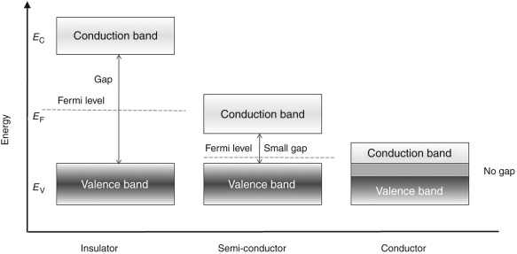
Fig 2: Energy band for Conductors, Semi-conductors and Insulators
From the above figure the conductors (metals) have both the energy bands overlapping. This shows that they have large number of free electrons which make them the good conductors.
There is one more energy band shown above having a huge gap between CB and VB which significantly shows that we need to provide large amount of energy to the electrons to jump from VB to CB. But this amount of energy is not possible to be applied and hence no movement of electron is seen. There is no conduction possible making them insulators.
The last one seen from above figure has a difference in CB and VB but the energy gap is such that after applying external voltage some of the electrons can jump from VB to CB. These are semi-conductors which can be made to conduct as conductors by exciting them externally.
Key takeaway
S.No | Conductors | Semiconductors | Insulators |
1 | Easily conducts the electrical current. | Conducts the electric current less than conductor and greater than insulator | Does not conduct any current |
2 | Has only one valence electron in its outermost orbit. | Has four valence electron in its outermost orbit | Has eight valence electron in its outermost orbit. |
3 | Conductor formed using metallic bonding | Semiconductors are formed due to covalent bonding | Insulators are formed due to ionic bonding. |
4 | Valence and conduction bands are overlapped | Valence and conduction bands are separated by forbidden energy gap of 1.1eV | Valence and conduction bands are separated by forbidden energy gap of 6 to 10eV |
5 | Resistance is very small | Resistance is high | Resistance is very high |
6 | It has positive temperature coefficient | It has negative temperature coefficient | It has negative temperature coefficient |
7 | Ex.copper,aluminium, etc | Ex. Silicon, germanium, etc | Ex. Mica, Paper, etc |
MOBILITY
The drift velocity produced per unit electric field is called 'mobility' , Thus Mobility is obviously a central parameter in characterizing electron and hole transport due to drift.
μ =  or μE =
The word mobility refers to freedom of movement. Analogously, in semiconductor work the mobility parameter is a measure of the ease of carrier motion in a crystal. Increasing the motion-impeding collisions within a crystal decreases the mobility of the carriers.
In other words, the carrier mobility varies inversely with the amount of scattering taking place within the semiconductor.
Lattice scattering involving collisions with thermally agitated lattice atoms, and ionized impurity (i.e., donor-site and/or acceptor-site) scattering. Relative to lattice scattering, it should be emphasized that it is the thermal vibration, the displacement of lattice atoms from their lattice, positions, that leads to carrier scattering. The internal field associated with the stationary array of atoms in a crystal is already taken into account in the effective mass formulation.
μ = q /m*
/m*
Where  is the mean free time between collisions and m* is the conductivity effective mass.
However,μ is also noted to vary inversely with the carrier effective mass—lighter carriers move more readily.
The carrier mobilities are essentially independent of the doping concentration. For dopings in excess of l015/cm3, the mobilities monotonically decrease with increasing NA or ND.
The mobilities of carrier depend upon temperature as μ . For Electrons μe
 and for holes μp

Conductivity
The conductivity of a material depends upon the concentration of free electrons. In semiconductors the concentration of electrons is in between conductors and insulators. As discussed in earlier section that the conduction in semiconductor is possible up to some temperature. Germanium and silicon are generally used semiconductors. If we talk about Ge than it has 4 electrons in its outer most shell which can form covalent bond with four adjacent Ge atoms.
At absolute zero the semiconductors behave as insulators as there are no free electrons for conduction. At room temperature due to presence of some energy few covalent bonds break and there are some free electrons. These free electrons contribute in conduction. For Ge the energy required to break the covalent bond is 0.72eV. For Si the energy required to break the covalent bond is 1.1eV at room temperature.
In semiconductors the holes can also be considered as the carrier of electricity. The hole exists in semiconductors where there is incomplete bond. When an electron leaves its place and to form bond with neighbouring atom it creates a new hole at that place. This process continues as every time due to electrons a new hole is created. So, it can be visualized as the holes move in opposite direction to the electrons. In ideal case the semiconductor has equal number of holes and electrons.
The current density due to drift holes for applied field E is given as
Jh=q p pE
pE
The current density due to drift electrons for applied field E is given as
Je = q pn n E
n E
The drift current density is given as
J= Jp+Jn
J = q (p p+n
p+n n) E
n) E
J= E
E
 =q (p
=q (p p+n
p+n n)
n)
Where
 = Conductivity of semiconductors
n, p = magnitude of free electron and hole concentration respectively.
Examples
Q1) For a p-type Ge ni = 2.1x10¹⁹m-3 density of boron =3.2x10²³ atoms m-3. The electron and hole mobility are 0.4 and 0.2 m2V-1s-1. Calculate conductivity before and after addition of boron?
Sol: Before adding boron
 =q (p
=q (p p+n
p+n n)
n)
= ni q ( p+
p+ n) = 2.1x1019x1.6x10-19x(0.4+0.2)=2.016 S/m-1
After adding boron
 =q p
=q p p
p
= 3.2x1023x1.6x10-19x0.2=10.24x10³S/m-1
Q2) Determine the density of the donor atoms which have been added to the intrinsic Ge to make it a n-type material of resistivity 0.1x10⁻²ohm-m. Mobility of electron in n-type semiconductor is 0.5m2V-1s-1.
Sol:  =q (n
=q (n n)
n)
n=  /q
/q n
n
 = 1/
= 1/
n= 1/ q
q n = 1/(0.1x10-2x0.5x1.6x10-19) = 1.25x10²²m-3
Q3) The intrinsic carrier density at room temperature in Ge is 3.4x10¹⁹m-3. If electron and hole mobilities are 0.4 and 0.2 m2V-1s-1 respectively. Calculate its resistivity?
Sol:  = 1/
= 1/
 =ni q (
 p+
p+ n) = 3.4x1019x 1.6x10-19(0.4+0.2) = 3.264S/m-1
 = 1/
= 1/ = 1/3.264 = 0.31ohm-m
Q4) The electron and hole mobilities in In-Sb are 6 and 0.2 m2V-1s-1 respectively. At room temperature resistivity of In-Sb is 2x10⁻⁴ohm-m. Find intrinsic carrier concentration assuming the material to be intrinsic?
Sol:  = 1/
= 1/
 =ni q (
 p+
p+ n)
n)
ni = 1/ q (
q ( p+
p+ n) = 1/2x10-4x1.6x10-19(6+0.2) = 5.04x10²¹m-3
Q5) An electric field of 90Vm-1 is applied to n-type semiconductor. Determine the current density in sample given electron mobility 0.4 m2V-1s-1, n=5.9x10²⁰m-3?
Sol: J= E
E
 = nq
= nq n = 5.9x1020x1.6x10-19x0.4=37.36S/m-1
J=3.39x10³
Q6) Determine the density of the donor atoms which have been added to the intrinsic Ge to make it a n-type material of resistivity 0.5x10⁻²ohm-m. Mobility of electron in n-type semiconductor is 0.8m2V-1s-1.
Sol:  =q (n
=q (n n)
n)
n=  /q
/q n
n
 = 1/
= 1/
n= 1/ q
q n = 1/(0.5x10-2x0.8x1.6x10-19) = 1.56x10²¹m-3
Semiconductors
Semiconductors are materials that have conductivity between conductors and insulators.
Semiconductors can be pure elements, such as silicon or germanium, or compounds such as gallium arsenide or cadmium selenide.
They are not good conductors nor good insulators as their name “semi”-conductors.
These materials such as silicon (Si), germanium (Ge), and gallium arsenide (GaAs), have electrical properties somewhere in the middle, between those of a “conductor” and an “insulator”.
They have very few “free electrons” because their atoms are closely grouped in a crystalline pattern called a “crystal lattice” but electrons are still able to flow, but only under special conditions.
There are two basic groups or classifications that can be used to define the different semiconductor types:
- Intrinsic Semiconductor
- Extrinsic Semiconductor
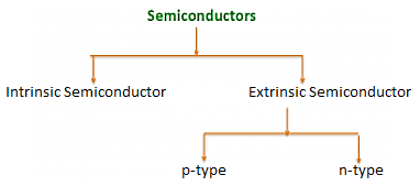
Figure 3: Type of semiconductor
The semiconductor is divided into two types. One is an Intrinsic Semiconductor and the other is an Extrinsic semiconductor. The pure form of the semiconductor is known as the intrinsic semiconductor and the semiconductor in which intentional impurities are added for making it conductive is known as the extrinsic semiconductor.
The conductivity of the intrinsic semiconductor becomes zero at room temperature while the extrinsic semiconductor is very little conductive at room temperature. The detailed explanation of the two types of the semiconductor is given below.
INTRINSIC SEMICONDUCTOR
An intrinsic type of semiconductor material made to be very pure chemically. As a result, it possesses a very low conductivity level having very few charge carriers, namely holes and electrons, which it possesses in equal quantities.
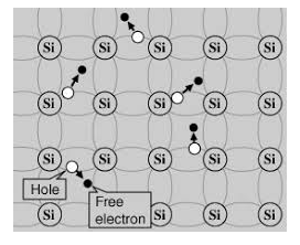
Figure 4: Intrinsic Semiconductor
The most commonly used semiconductor basics material by far is silicon. Silicon has four valence electrons in its outermost shell which it shares with its neighbouring silicon atoms to form a full orbital of eight electrons. The structure of the bond between the two silicon atoms is such that each atom shares one electron with its neighbour making the bond very stable.
As there are very few free electrons available to move around the silicon crystal, crystals of pure silicon (or germanium) are therefore good insulators. Silicon atoms are arranged in a definite symmetrical pattern making them a crystalline solid structure. A crystal of pure silica (silicon dioxide or glass) is generally said to be an intrinsic crystal (it has no impurities) and therefore has no free electrons.
An extremely pure semiconductor is called an Intrinsic Semiconductor. Based on the energy band phenomenon, an intrinsic semiconductor at absolute zero temperature is shown below.
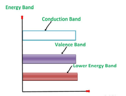
Figure 5: Intrinsic semiconductor at absolute zero temperature.
Its valence band is filled and the conduction band is empty. When the temperature is raised and some heat energy is supplied to it, some of the valence electrons are lifted to the conduction band leaving behind holes in the valence band as shown below.
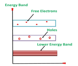
Figure 6: Intrinsic semiconductor at T >0
A hole is the absence of an electron in a particular place in an atom. Although it is not a physical particle in the same sense as an electron, a hole can be passed from atom to atom in a semiconductor material. It is considered to have a positive charge. Holes are positive charge carriers.
The electrons reaching the conduction band move randomly. The holes created in the crystal also free to move anywhere.
This behaviour of the semiconductor shows that they have a negative temperature coefficient of resistance. This means that with the increase in temperature, the resistivity of the material decreases, and the conductivity increases.
But simply connecting a silicon crystal to a battery supply is not enough to extract an electric current from it. To do that we need to create a “positive” and a “negative” pole within the silicon allowing electrons and therefore electric current to flow out of the silicon. These poles are created by doping the silicon with certain impurities.
DOPING
The process by which an impurity is added to a semiconductor is known as Doping. The amount and type of impurity which is to be added to the material have to be closely controlled during the preparation of extrinsic semiconductor. Generally, one impurity atom is added to 108 atoms of a semiconductor.
The purpose of adding impurity in the semiconductor crystal is to increase the number of free electrons or holes to make it conductive.
If a Pentavalent impurity, having five valence electrons is added to a pure semiconductor a large number of free electrons will exist. Which makes an n-type extrinsic semiconductor.
If a trivalent impurity having three valence electrons is added, a large number of holes will exist in the semiconductor. Which makes a p-type extrinsic semiconductor.
EXTRINSIC SEMICONDUCTOR
Extrinsic types of semiconductors are those where a small amount of impurity has been added to the basic intrinsic material. This 'doping' uses an element from a different periodic table group and in this way, it will either have more or fewer electrons in the valence band than the semiconductor itself. This creates either an excess or shortage of electrons. In this way two types of semiconductors are available: Electrons are negatively charged carriers. Holes are positively charged carriers.
Depending upon the type of impurity added the extrinsic semiconductor may be classified as an n-type semiconductor and p-type semiconductor.
P-TYPE EXTRINSIC SEMICONDUCTOR
The extrinsic p-Type Semiconductor is formed when a trivalent impurity is added to a pure semiconductor in a small amount, and as a result, a large number of holes are created in it. A large number of holes are provided in the semiconductor material by the addition of trivalent impurities like Gallium and Indium. Such type of impurities which produce a p-type semiconductor is known as an Acceptor Impurities because each atom of them creates one hole which can accept one electron.
In a P-type semiconductor material, there is a shortage of electrons, i.e. there are 'holes' in the crystal lattice. Electrons may move from one empty position to another and in this case, it can be considered that the holes are moving. This can happen under the influence of a potential difference and the holes can be seen to flow in one direction resulting in an electric current flow. It is harder for holes to move than for free electrons to move and therefore the mobility of holes is less than that of free electrons. Holes are positively charged carriers.
A trivalent impurity like Aluminium, having three valence electrons is added to Silicon crystal in a small amount. Each atom of the impurity fits in the Silicon crystal in such a way that its three valence electrons form covalent bonds with the three surrounding Silicon atoms as shown in the figure below.

Figure 7: p-Type Semiconductor
ENERGY BAND DIAGRAM OF P-TYPE SEMICONDUCTOR
The energy band diagram of a p-Type Semiconductor is shown below.
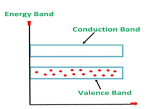
Figure 8: Energy band diagram of a p-Type Semiconductor
A large number of holes or vacant space in the covalent bond is created in the crystal with the addition of the trivalent impurity. A small or minute quantity of free electrons is also available in the conduction band.
They are produced when thermal energy at room temperature is imparted to the Silicon crystal-forming electron-hole pairs. But the holes are more in number as compared to the electrons in the conduction band. It is because of the predominance of holes over electrons that the material is called a p-type semiconductor. The word “p” stands for positive material.
CONDUCTION THROUGH P TYPE SEMICONDUCTOR
In p-type semiconductors, a large number of holes are created by the trivalent impurity. When a potential difference is applied across this type of semiconductors.
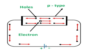
Figure 9: Conduction through p type semiconductor
The holes are available in the valence band are directed towards the negative terminal. As the current flow through the crystal is by holes, which are a carrier of positive charge, therefore, this type of conductivity is known as positive or p-type conductivity. In a p-type conductivity, the valence electrons move from one covalent to another.
The conductivity of an n-type semiconductor is nearly double that of a p-type semiconductor. The electrons available in the conduction band of the n-type semiconductor are much more movable than holes available in the valence band in a p-type semiconductor. The mobility of holes is poor as they are more bound to the nucleus.
Even at room temperature, the electron-hole pairs are formed. These free electrons which are available in minute quantity also carry a little amount of current in the p-type semiconductors.
N-TYPEEXTRINSIC SEMICONDUCTOR
When a few Pentavalent impurities such as Phosphoruswhose atomic number is 15, which is categorized as 2, 8, and 5. It has five valence electrons, which are added to silicon crystals. Each atom of the impurity fits in four silicon atoms as shown in the figure below.
Hence, each Arsenic atom provides one free electron in Silicon crystal. Since an extremely small amount of Phosphorus, impurity has a large number of atoms; it provides millions of free electrons for conduction.
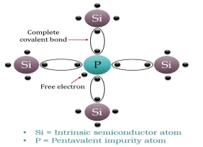
Figure 10: N-type semiconductor
An N-type semiconductor material has an excess of electrons. In this way, free electrons are available within the lattices, and their overall movement in one direction under the influence of a potential difference results in an electric current flow. This is an N-type semiconductor, the charge carriers are electrons.
ENERGY DIAGRAM OF N-TYPE SEMICONDUCTOR
A large number of free electrons are available in the conduction band because of the addition of the Pentavalent impurity. These electrons are free electrons that did not fit in the covalent bonds of the crystal. However, a minute quantity of free electrons is available in the conduction band forming hole- electron pairs.
The Energy diagram of the n-type semiconductor is shown in the figure below.
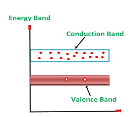
Figure 11: Energy diagram of the n-type semiconductor
- The addition of pentavalent impurity results in a large number of free electrons.
- When thermal energy at room temperature is imparted to the semiconductor, a hole-electron pair is generated and as a result, a minute quantity of free electrons is available. These electrons leave behind holes in the valence band.
- Here n stands for negative material as the number of free electrons provided by the pentavalent impurity is greater than the number of holes.
CONDUCTION THROUGH N-TYPE SEMICONDUCTOR
In the n-type semiconductor, a large number of free electrons are available in the conduction bands which are donated by the impurity atoms. The figure below shows the conduction process of an n-type semiconductor.
When a potential difference is applied across this type of semiconductor, the free electrons are directed towards the positive terminals. It carries an electric current. As the flow of current through the crystal is constituted by free electrons which are carriers of a negative charge, therefore, this type of conductivity is known as negative or n-type conductivity.
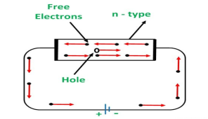
Figure 12: Conduction through n-type semiconductor
The electron-hole pairs are formed at room temperature. These holes which are available in small quantities in the valence band also consist of a small amount of current. For practical purposes, this current is neglected.
Key Takeaways
- Semiconductors are materials that have conductivity between conductors and insulators.
- The semiconductor is divided into two types. One is an Intrinsic Semiconductor and the other is an Extrinsic semiconductor.
- The pure form of the semiconductor is known as the intrinsic semiconductor
- The semiconductor in which intentional impurities are added for making it conductive is known as the extrinsic semiconductor.
- A hole is the absence of an electron in a particular place in an atom.
- The process by which an impurity is added to a semiconductor is known as Doping.
- Depending upon the type of impurity added the extrinsic semiconductor may be classified as an n-type semiconductor and p-type semiconductor.
- The extrinsic p-Type Semiconductor is formed when a trivalent impurity is added to a pure semiconductor in a small amount, and as a result, a large number of holes are created in it.
- The extrinsic n-Type Semiconductor is formed when a Pentavalent impurity is added to a pure semiconductor in a small amount, and as a result, a large number of electrons are created in it.
Fermi level" is the term used to describe the top of the collection of electron energy levels at absolute zero temperature. This concept comes from Fermi-Dirac statistics. Electrons are fermions and by the Pauli exclusion principle cannot exist in identical energy states. So, at absolute zero they pack into the lowest available energy states and build up a "Fermi sea" of electron energy states. The Fermi level is the surface of that sea at absolute zero where no electrons will have enough energy to rise above the surface.
The concept of the Fermi energy is a crucially important concept for the understanding of the electrical and thermal properties of solids. Both ordinary electrical and thermal processes involve energies of a small fraction of an electron volt. But the Fermi energies of metals are on the order of electron volts. This implies that the vast majority of the electrons cannot receive energy from those processes because there are no available energy states for them to go to within a fraction of an electron volt of their present energy. Limited to a tiny depth of energy, these interactions are limited to "ripples on the Fermi sea".
At higher temperatures a certain fraction, characterized by the Fermi function, will exist above the Fermi level. The Fermi level plays an important role in the band theory of solids. In doped semiconductors, p-type and n-type, the Fermi level is shifted by the impurities, illustrated by their band gaps. The Fermi level is referred to as the electron chemical potential in other contexts.
The Fermi energy also plays an important role in understanding the mystery of why electrons do not contribute significantly to the specific heat of solids at ordinary temperatures, while they are dominant contributors to thermal conductivity and electrical conductivity. Since only a tiny fraction of the electrons in a metal are within the thermal energy kT of the Fermi energy, they are "frozen out" of the heat capacity by the Pauli principle. At very low temperatures, the electron specific heat becomes significant.
It is named after the Physicist Enrico Fermi. A Fermi level is the measure of the energy of least tightly held electrons within a solid. It is important in determining the thermal and electrical properties of solids. It can be defined as:
The Fermi energy is a concept in quantum mechanics usually refers to the energy difference between the highest and lowest occupied single-particle states in a quantum system of non-interacting fermions at absolute zero temperature.
The value of the Fermi level at absolute zero temperature is known as the Fermi energy. It is also the maximum kinetic energy an electron can attain at 0K. Fermi energy is constant for each solid.
To determine the lowest possible Fermi energy of a system, we first group the states with equal energy into sets and arrange them in increasing order of energy. We then add particles one at a time, successively filling up the unoccupied quantum states with the lowest energy.
When all the particles are arranged accordingly, the energy of the highest occupied state is the Fermi energy.
In Spite of the extraction of all possible energy from metal by cooling it to near absolute zero temperature (0 Kelvin), the electrons in the metal still move around. The fastest ones move at a velocity corresponding to a kinetic energy equal to the Fermi energy.
The highest energy level that an electron can occupy at the absolute zero temperature is known as the Fermi Level. The Fermi level lies between the valence band and conduction band because at absolute zero temperature the electrons are all in the lowest energy state. Due to lack of sufficient energy at 0 Kelvin, the Fermi level can be considered as the sea of fermions (or electrons) above which no electrons exist. The Fermi level changes as the solids are warmed and as electrons are added to or withdrawn from the solid.
Don’t get confuse between Fermi level and Fermi energy. Both the terms are equal at absolute zero temperature but they are different at other temperature.
Derivation of the expression for Fermi energy
Let us recall the formula for density of states (we derived density of states under article 5.4, equation 7)
Density of States, N(E) dE = π/4h3 (8m)3/2 E1/2dE
Each electron energy level can accommodate two electrons as per Pauli’s exclusion principle. (Spin up and Spin down = 2 (e) × density of states).
N(E)dE = 2 N(E) dE
N(E) dE = 2 π/4h3 (8m)3/2 E1/2 dE F(E)
N(E) dE = π/2h3 (8m)3/2 E1/2 dE F(E)
Carrier Concentration in Metals
Let N(E) dE represents the number of filled energy states between the interval of energy dE, normally all the energy states will not be filled
DN = N(E) dE F(E)
DN = 2 π/4h3 (8m)3/2 E1/2 dE F(E)
The actual number of electrons in dE, F(E) = 1
DN = π/2h3 (8m)3/2 E1/2dE
Normally all the states are not filled states, filling of electrons is a given energy state is given by Fermi-function F(E). Let dn represents the number of filled energy states.
In this case of material of absolute zero the upper occupied level is EF and for all the levels below EF, F(E)=1 (at T = 0 K the maximum energy level that can be occupied by the electron is called Fermi energy level EF T = 0 K F(E) = 1).
Integrating equation (8) within the limits 0 to EF0 us can get the number of energy states of electron (N)


Hence the Fermi energy of a metal depends only on the density of electrons of that metal.
In metals, the Fermi energy gives us information about the velocities of the electrons which participate in ordinary electrical conduction. The amount of energy which can be given to an electron in such conduction processes is on the order of micro-electron volts (see copper wire example), so only those electrons very close to the Fermi energy can participate. The Fermi velocity of these conduction electrons can be calculated from the Fermi energy.
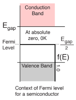
Figure 13: Fermi level for a Semiconductor
vF = 
This speed is a part of the microscopic Ohm's Law for electrical conduction. For a metal, the density of conduction electrons can be implied from the Fermi energy
Key Takeaways
- The highest energy level that an electron can occupy at the absolute zero temperature is known as the Fermi Level.
- The Fermi energy is a concept in quantum mechanics usually refers to the energy difference between the highest and lowest occupied single-particle states in a quantum system of non-interacting fermions at absolute zero temperature.
- Fermi energy of a metal depends only on the density of electrons of that metal. It is given by

4. The Fermi velocity of these conduction electrons can be calculated from the Fermi energy by using the following relation.
vF = 
FORMATION OF ENERGY BANDS IN SOLIDS
Let us begin the conceptual path leading to the energy band model by recalling the situation inside an isolated Si atom. Ten of the 14 electrons inside an isolated Si atom are tightly bound to the nucleus and are unlikely to be significantly perturbed by normal atom—atom interactions. The remaining four electrons are rather weakly bound and, if unperturbed, occupy four of the eight allowed energy states immediately above the last core level. Moreover, it is implicitly understood that the electronic energy states within a group of Si atoms, say N Si atoms, are all identical -as long as the atoms are isolated, that is, far enough apart so that they are non-interacting.
If N atoms are brought into close proximity it is quite reasonable to expect a modification in the energy states of the valence electrons. Starting with N-isolated Si atoms, and conceptually bringing the atoms closer and closer together, one finds the interatomic forces lead to a progressive spread in the allowed energies. The spread in energies gives rise to closely spaced sets of allowed-states is known as energy bands.
An isolated atom possesses discrete energies of different electrons. Suppose two isolated atoms are brought to very close, then the electrons in the orbits of two atoms interact with each other. So, that in this system, the energies of electrons will not be in the same level but changes and the energies will be slightly lower and larger than the original value. So, at the place of each energy level, a closely spaced two energy levels exists.
If ‘N’ number of atoms are brought together to form a solid and if these atoms’ electrons interact and give ‘N’ number of closely spaced energy levels in the place of discrete energy levels, it is known as bands of allowed energies. Between the bands of allowed energies, there are empty energy regions, called forbidden band of energies.

Figure 14: Formation of energy bands in solids
Kronig-Penney model shows the existence of band gap. Kronig-Penney model supports the existence of these bands of energies (allowed bands and forbidden bands).
The formation of energy bands has been explained taking Sodium (Na) metal as an example. When isolated sodium atoms are brought together to form a solid, then the energy levels of the valence electrons spread into bands. The 3S and 3P orbitals electrons energies are shown in Figure 3. These bands are seen to overlap strongly at the interatomic spacing of sodium.
We know that atoms have discrete energy levels. When a huge number of atoms are combined to form a solid, these discrete energy levels are replaced by discrete ranges of energy or called as energy bands.
In energy bands there are so many individual allowed energy values or you can say that the energy bands the energy distribution is continuous. This is shown in the following figure
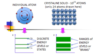
Figure 15: Energy Level and energy band
In between energy bands are ranges of energy which are entirely impossible known as band gaps
Different substances have different band structures which explain the characteristics of that substance in terms of electrical conduction.
Bands are formed by the closely spaced orbitals.
There are three types of bands:
1. Valance Bands: Valence band it is a group of orbitals which contain electrons in the shell. Or we can say It is also defined as the energy band that comprises of valence electrons present in the outermost shell of an atomic structure.
These valence electrons, when provided with sufficient energy, get changed into free electrons and moves to conduction band thereby causing conductivity. It is at a lower energy level than the conduction band in the energy level diagram.
2. Conduction Band: Conduction band is a group of empty orbitals of the shells that do not contain any electron due to their configuration making the orbitals of higher energy levels.
When the electrons pass from valance band to the conduction band these solids conduct electricity with flow of charges in the form of electrons.
3. Forbidden Energy Band: These two bands are separated by a certain amount of energy known as the forbidden energy gap. In this band not a single electron is available. It diagram it is named as Band Gap.
ENERGY BAND DIAGRAM OF GERMANIUM & SILICON
Consider an isolated silicon atom; its energy levels are quantized. When two identical atoms are brought closer together, the quantized energy levels hybridize and split into two different levels because of the mutual interaction of the two atoms. More generally, when N atoms are moved closer, until they reach the equilibrium inter-atomic distance d, the energy levels split into N levels. These N levels are very close to each other if N is large (which is the case in a crystal) so that they eventually form a continuous energy band.
Germanium was discovered in 1886. It is an earth element from the flue dust of zinc smelters. The recovered germanium is in the form of germanium dioxide powder. It is then converted into pure germanium. Its atomic number is 32. It has 32 protons in the nucleus and 32 electrons distributed in the four orbits around the nucleus. The number of electrons in the first, second, third and fourth orbit is 2, 8, 18 and 4 respectively. It is clear that the germanium has four valence electrons. The various germanium atoms are held together through covalent bonds.
The forbidden energy gap (i.e. the gap between the valence band and conduction band) in this material is very small. Hence, very small energy is sufficient to lift the electrons from the valence band to the conduction band.
Energy band diagram for germanium is given in figure
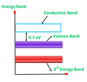
Figure 16: Energy band diagram of germanium
Silicon is the element available in most of the common rocks. Actually, sand is silicon dioxide. It is treated chemically and reduced to pure silicon, which can be used for the preparation of electronic devices. Ts atomic number is 14. Therefore, it has 14 protons in the nucleus and 14 electrons distributed in the three orbits around the nucleus. The number of electrons in the first, second and third orbit is 2, 8 and 4 respectively. The various silicon atoms are held together through covalent bonds.
The forbidden energy gap in this material is quite small. It also needs small energy to lift the electrons from the valence band to the conduction band.
Therefore, even at room temperature, a minute quantity of valence electrons is lifted to the conduction band and constitute current conduction if a high electric field is applied. However, at room temperature, the number of electrons lifted to the conduction band in the case of silicon is quite less than germanium.
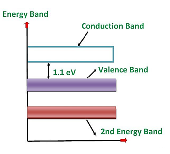
Figure 17: Energy band diagram of silicon
Key Takeaways
- Energy Bond Model gives the energy aspect of atoms to get good knowledge of semiconductor.
- The spread in energies gives rise to closely spaced sets of allowed-states is known as energy bands.
- Bands are formed by the closely spaced orbitals.
- There are three types of bands: Valence band, conduction band, Forbidden Energy Band
- The Valence band and conduction band are separated by a certain amount of energy known as the forbidden energy gap.
- Insulators are those having wide band gap.
- Metals: very small or no band gap exists at all due to an overlap of the valence and conduction bands
- Semiconductors is an intermediate case
A P-N Junction Diode is formed by doping one side of a piece of silicon with a P-type dopant (Boron) and the other side with a N-type dopant (phosphorus). Ge can be used instead of Silicon. The P-N junction diode is a two-terminal device. This is the basic construction of the P-N junction diode. It is one of the simplest semiconductor devices as it allows current to flow in only one direction.
ZERO BIASED CONDITION
In this case, no external voltage is applied to the P-N junction diode; and therefore, the electrons diffuse to the P-side and simultaneously holes diffuse towards the N-side through the junction, and then combine with each other. Due to this an electric field is generated by these charge carriers. The electric field opposes further diffusion of charged carriers so that there is no movement in the middle region. This region is known as depletion width or space charge.

Figure 18: Unbiased or zero biased PN Junction Diode
FORWARD BIAS
In the forward bias condition, the positive terminal of the battery is connected to the P-Type material and the negative terminal of the battery is connected to the N-type material. This connection is also called as giving positive voltage.
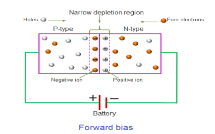
Figure 19: Forward bias
Electrons from the N-region cross the junction and enters the P-region. Due to the attractive force that is generated in the P-region the electrons are attracted and move towards the positive terminal. Simultaneously the holes are attracted to the negative terminal of the battery. By the movement of electrons and holes current flows. In this condition, the width of the depletion region decreases due to the reduction in the number of positive and negative ions.
If this external voltage Vf becomes greater than the value of the potential barrier, approx. 0.7 volts for silicon and 0.3 volts for germanium, the potential barriers opposition will be overcome and current will start to flow.
This is because the negative voltage pushes or repels electrons towards the junction giving them the energy to cross over and combine with the holes being pushed in the opposite direction towards the junction by the positive voltage. This results in a characteristics curve of zero current flowing up to this voltage point, called the “knee” on the static curves and then a high current flow through the diode with little increase in the external voltage as shown in I-V characteristics.
REVERSE BIAS
In the reverse bias condition, the negative terminal of the battery is connected to the P-type material and the positive terminal of the battery is connected to the N-type material. This connection is also known as giving negative voltage.
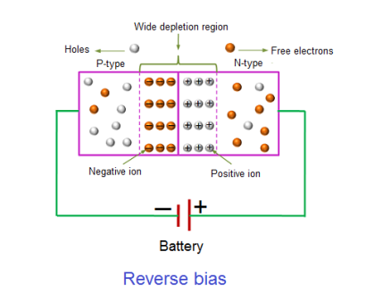
Figure 20: Reverse bias
The positive voltage applied to the N-type material attracts electrons towards the positive electrode and away from the junction, while the holes in the P-type end are also attracted away from the junction towards the negative electrode.
The net result is that the depletion layer grows wider due to a lack of electrons and holes and presents a high impedance path, almost an insulator. The result is that a high potential barrier is created thus preventing current from flowing through the semiconductor material.
This condition represents a high resistance value to the PN junction and practically zero current flows through the junction diode with an increase in bias voltage. However, a very small leakage current does flow through the junction which can be measured in micro-amperes, (μA).
If the reverse bias voltage Vr applied to the diode is increased to a sufficiently high enough value, it will cause the diode’s PN junction to overheat and fail due to the avalanche effect around the junction. This may cause the diode to become shorted and will result in the flow of maximum circuit current, and this shown as a step downward slope in the reverse static characteristics curve in I-V characteristics.
I-V CHARACTERISTICS OF PN JUNCTION DIODE
The I-V Characteristic Curves, which is short for Current-Voltage Characteristic Curves or simply I-V curves of an electrical device
The application of a forward biasing voltage on the junction diode results in the depletion layer becoming very thin and narrow which represents a low impedance path through the junction thereby allowing high currents to flow. The point at which this sudden increase in current takes place is represented on the static I-V characteristics curve above as the “knee” point. The current starts increasing with increase in voltage. At knee voltage current shows a sharp increment in its magnitude. This behaviour is mentioned above. As large current flow in forward biasing so we measure this current in mA.
When a junction diode is Reverse Biased, the thickness of the depletion region increases and the diode acts like an open circuit blocking current flow. So only a very small leakage current will flow.
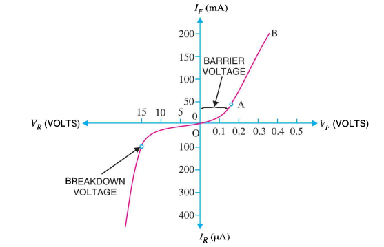
Figure 21: I-V characteristics
Note in addition that the minority carrier drift currents are not affected by the height of the potential bill. It is the number of minority carriers wandering into the depletion region per second that determines the current flow.
The situation is similar to a waterfall. The water flowing over the falls is independent of the height of the falls. The overall 1-V dependence is concluded to be of the general form 1-V characteristics.
I = I0 ( ..............(1)
Equation (1) is identical to the ideal diode equation if VA is set equal to kT/q.
Key Takeaways
A P-N Junction Diode is formed by doping one side of a piece of silicon with a P-type dopant (Boron) and the other side with a N-type dopant (phosphorus). Ge can be used instead of Silicon.
Zero biased condition is the case when no external voltage is applied to the P-N junction diode.
In the forward bias condition, the positive terminal of the battery is connected to the P-Type material and the negative terminal of the battery is connected to the N-type material. This connection is also called as giving positive voltage.
In the reverse bias condition, the negative terminal of the battery is connected to the P-type material and the positive terminal of the battery is connected to the N-type material. This connection is also known as giving negative voltage.
The ideal diode equation represents current flow through an ideal p-n junction diode as a function of applied voltage.
In realistic settings, current will deviate slightly from this ideal case. We know that ap-n junction diode creates the following current:
Under reverse bias, there is a small, constant reverse current, and under forward bias, there is a forward current that increases with voltage.
The current-voltage function (also called the "i-v characteristic") for an ideal diode is
i(v) = IS[exp(v /ηVT) - 1], v>VZ
WhereISis the reverse saturation current,
v is the applied voltage
VT = T / 11,586 is the volt equivalent of temperature
η is the emission coefficient, which is 1 for germanium devices and 2 for silicon devices.
i is defined as positive when flowing from p to n. This is also called the Shockley ideal diode equation or the diode law.
For v ≤ VZ, the diode is in breakdown and the ideal diode equation no longer applies;
For v ≤ VZ, i = -∞. The ideal diode i-v characteristic curve is shown below:
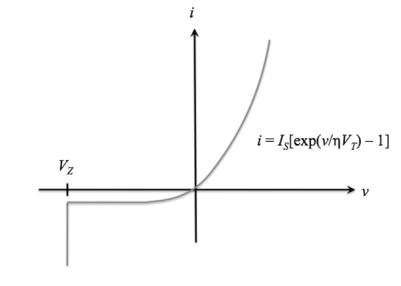
Figure 22. Ideal diode equation
The diodes are used as clipper, clampers and as rectifiers. All these applications are discussed in this and further sections
Clipper
The clipper circuits are basically used to clip the portion of any input signal without changing or distorting the remaining part of the input waveform.
Positive Diode Clipping Circuits

As we see from the above figure the diode is forward biased during the positive half cycle of the input sinusoidal waveform. But the PN junction diode starts conducting after it crosses the cut off voltage. As we already know it should be greater than 0.7volts and 0.3 volts for Si and Ge diodes respectively.
The diode conducts for a complete positive half cycle and maintains the voltage across itself until the sinusoidal waveform falls below the value. As the diode conducts the output here is clipped.
For the negative half cycle the diode becomes reversed biased and a reverse current of very small amount flows across the diode. Hence, we can say that there is no voltage change in this case due to no flow of current. Therefore, the output is unaltered in this and is equal to the input applied voltage.
Negative Diode Clipping Circuits

As we see from the above figure the diode is reverse biased during the positive half cycle of the input sinusoidal waveform. But the PN junction diode acts as an open circuit. The output in this case is equal to the input applied voltage.
For the negative half cycle the diode becomes forward biased and starts to conduct. Hence, we can say that there is no voltage at the output due to no flow of current.
Clipping of Both Half Cycles

Now if we connect two diodes both reverse to each other in parallel then the output is clipped in both the half cycles. The diode D1 clips the positive half cycle the same as it does in the positive clipper. The diode D2 clips the negative half cycle the same as it does in the negative clipper.
They are used as voltage limiter circuits.
CLAMPER
The clamper circuit shifts the waveform to a different dc level without changing the applied signal level. The circuit consists of a capacitor, a diode and a resistor.
This is also called a level shifter because we can shift the level of the signal by using a clamping circuit.
As the circuit consists of a capacitor connected parallel across the load. The capacitor circuit depends upon the time constant of the capacitor. The capacitor charges when the diode is forward biased and starts conducting. The capacitor should not discharge drastically when the diode is reverse biased. There are two types of clamper circuits i.e positive and negative clampers.
Negative Clamper
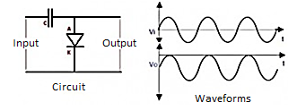
The diode conducts in the positive half cycle as it is forward biased and the capacitor charges. In the negative half cycle the output is the sum of input voltage and voltage stored across the capacitor.
Positive Clamper
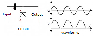
In this the diode is connected in the opposite direction than in the negative clamper. In this case the output voltage is the sum of input voltage and capacitor voltage. The diode conducts in the negative half cycle and charges the capacitor. Hence, the voltage is clamped in a positive direction.
Half Wave rectifier
- It is the simplest form of the rectifier. Here, a single diode is used.
- It consists of an AC source, transformer (step-down), diode, and resistor (load).
- The diode is placed between the transformer and resistor (load).
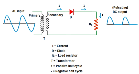
Operation:
- It allows only half cycle and blocks the other half cycle.
- When it allows positive half cycles and blocks negative half cycles, it is called a positive half wave rectifier. The output DC current or DC signal produced by a positive half wave rectifier is a series of positive half cycles or positive sinusoidal pulses.
- When it allows electric current during the negative half-cycle of input AC signal and blocks electric current during the positive half-cycle of the input AC signal.
- A negative half wave rectifier produces a series of negative sinusoidal pulses.
- For an ideal diode, the positive half cycle or negative half cycle at the output is exactly same.
Characteristics of half wave rectifier
Ripple factor
The ripple factor is given as
 -1]
-1]
Finally, we get
γ = 1.21
Hence, the DC voltage is 121% of the DC magnitude.
DC current
The DC current is given by,
IDC=
Where,
Imax = maximum DC load current
Output DC voltage (VDC)
The output DC voltage is given by,
VDC=
Where, VSmax = Maximum secondary voltage
Rectifier efficiency
It is defined as the ratio of output DC power to the input AC power.
The rectifier efficiency of a half wave rectifier is 40.6%
Root mean square (RMS)
The root mean square (RMS) value of load current in a half wave rectifier is
IRMS=
The root mean square (RMS) value of output load voltage in a half wave rectifier is
VRMS = IRMS RL = Im/2 RL
Form factor
It is defined as the ratio of RMS value to the DC value given by,
F.F = RMS value / DC value
The form factor of a half wave rectifier is F.F = 1.57
TRANSFORMER UTILISATION FACTOR (TUF):-It indicates how well the ilp transformer is being utilized
TUF= DC O/P Power / AC power rating of the transformer

Key Takeaways:
- It allows only half cycle and blocks the other half cycle.
- When it allows positive half cycles and blocks negative half cycles, it is called a positive half wave rectifier and vice-versa.
Q. A half-wave rectifier is used to supply 50V d.c. To a resistive load of 800 Ω. The diode has a resistance of 25 Ω. Calculate a.c. Voltage required.
Solution:
Output voltage Vdc= 50V
Diode resistance rf=25
Load Resistance RL= 800 
Let Vm be the maximum value of ac voltage required
Vdc = Idc x RL
Vdc= Im/π x RL
Vdc= [Vm/ π x(rf+ RL)]RL
50= [Vm/ π x (25+800)]x800
Vm= 162V
The a.c voltage of maximum value 162V is required
Full Wave Rectifier
1) A centre tapped rectifier is a type of full wave rectifier that uses two diode connected to the secondary of a centre tapped transformer.
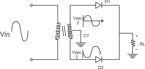
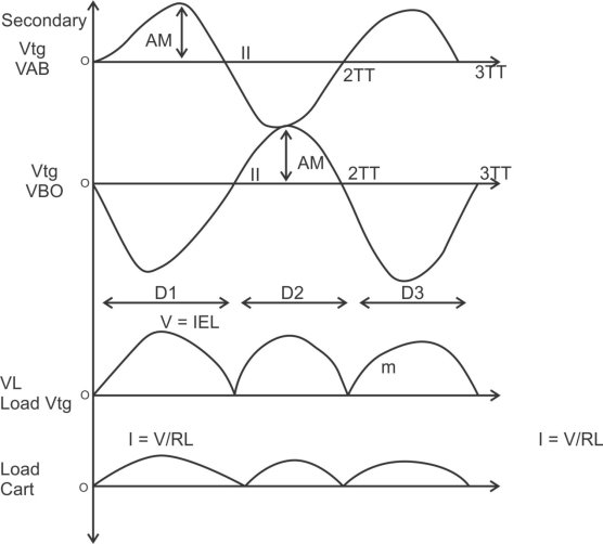
Center tapped full wave rectifier operation:-
I) During positive half cycle of i/p ac supply.
Diagram

D1.Is in forward biased & D2 is in reverse biased.
II)During -ve half cycle.

D1 Reverse biased
D2 Forward biased
ADVANTAGES
1) law ripple factor as Compared to HKR.
2)Better rectification efficiency.
3) Better TUF.
4)Higher value of average load voltage& average load circuit.
5)No possibility of transformer core saturation.
DISADVANTAGES
PIV of diode is 2vm, more size costly.
APPLICATION
I) Battery charges.
2)power supply at laboratory, high current, electronic circuit.
Key takeaway
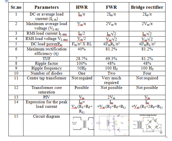
It uses four individual rectifying diodes which are connected in a closed loop called “bridge” configuration to produce the desired output.
It does not require a special centre tapped transformer, hence reducing its size and cost. The single secondary winding is connected one side to the diode bridge network and the other side to the load.
The four diodes D1 to D4 are arranged in “series pairs” and only two diodes conduct current during each half cycle.
During the positive half cycle, diodes D1 and D2 conduct in series while diodes D3 and D4 are reverse biased producing current through the load.
During the negative half cycle, diodes D3 and D4 conduct in series and diodes D1 and D2 are switched “OFF” as they become reverse biased producing current through the load.
During each half cycle the current flows through two diodes instead of just one. The ripple frequency is now twice the supply frequency.

Output Waveform:
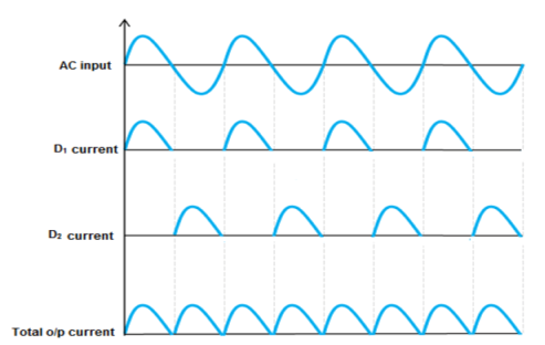
Characteristics of full wave rectifier
Ripple factor
The ripple factor is given by

Finally, we get γ = 0.48
Rectifier efficiency
It is defined as the ratio of DC output power to the AC input power.
It can be mathematically written as
η = output PDC / input PAC
The rectifier efficiency of a full wave rectifier is 81.2%.
It is the maximum voltage a diode can withstand in the reverse bias condition.
The peak inverse voltage (PIV) = 2Vsmax
DC output current
The current produced by D1 is Imax / π and the current produced by D2 is Imax / π.
So, the output current IDC = 2Imax / π
Where, Imax = maximum DC load current
DC output voltage
The DC output voltage appeared at the load resistor RL is given as
VDC = 2Vmax /π
Where,
Vmax = maximum secondary voltage
Root mean square (RMS) value of load current IRMS
The root mean square (RMS) value of load current in a full wave rectifier is

The root mean square (RMS) value of output load voltage in a full wave rectifier is

Form factor
It is the ratio of RMS value of current to the DC output current
F.F = RMS value of current / DC output current
The form factor of a full wave rectifier is F.F = 1.11
Advantages:
High rectifier efficiency
Low power loss
Low ripples
It has fewer ripples than the half wave rectifier.
Disadvantages:
High cost
The center tapped transformers are expensive and occupy a large space.
Key Takeaways:
- The process of converting the AC current into DC current is called rectification.
- When an additional wire is connected across the exact middle of the secondary winding of a transformer, it is known as a center tapped transformer.
- Bridge rectifier uses four individual rectifying diodes connected in a closed loop “bridge” configuration to produce the desired output.
Q) A full-wave rectifier uses two diodes, the internal resistance of each diode may
be assumed constant at 20 Ω. The transformer r.m.s. Secondary voltage from center tap to each end of secondary is 50 V and load resistance is 980 Ω. Find: (i) the mean load current (ii) the r.m.s. value of load current.
Solution:
Rf =20 , RL=980
Maximim ac voltage Vm=50√2=70.7V
Maximim load current Im=Vm/rf+RL= 70.7/(20+980)=70.7mA
Mean load current Idc= 2Im/π= 2x70.7/π= 45mA
RMS value of load current Irms=Im/√2= 70.7/√2=50mA
The satisfactory explanation of this breakdown of the junction was first given by the American scientist C. Zener. A Zener diode is a special type of diode that is designed to operate in the reverse breakdown region.
An ordinary diode operated in this region will usually be destroyed due to excessive current. This is not the case for the Zener diode.
It has already been discussed that when the reverse bias on a crystal diode is increased, a critical voltage, called breakdown voltage is reached where the reverse current increases sharply to a high value. The breakdown region is the knee of the reverse characteristic as shown in Figure 32.
The breakdown voltage is sometimes called Zener voltage and the sudden increase in current is known as Zener current.
The breakdown or Zener voltage depends upon the amount of doping. If the diode is heavily doped, depletion layer will be thin and consequently the breakdown of the junction will occur at a lower reverse voltage.
On the other hand, a lightly doped diode has a higher breakdown voltage. When an ordinary crystal diode is properly doped so that it has a sharp breakdown voltage, it is called a Zener diode. A properly doped crystal diode which has a sharp breakdown voltage is known as a Zener diode.
Figure shows the symbol of a Zener diode. It may be seen that it is just like an ordinal, diode except that the bar is turned into z-shape.

Figure 23: Symbol of a Zener diode
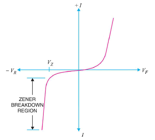
Figure 24: I-V characteristics of Zener diode
As the curve reveals, two things happen when Vz is reached:
- The diode current increases rapidly.
- The reverse voltage Vz across the diode remains almost constant.
The following points may be noted
(i) A Zener diode is like an ordinary diode except that it is properly doped so as to have a sharp breakdown voltage.
(ii) A Zener diode is always reverse connected i.e. it is always reverse biased.
(iii) A Zener diode has sharp breakdown voltage, called Zener voltage Vz.
(iv) When forward biased, its characteristics are just those of ordinary PN junction diode.
(v) The Zener diode is not immediately burnt just because it has entered the breakdown region. As long as the external circuit connected to the diode limits the diode current to less than burn out value, the diode will not burn out.
In other words, the Zener diode operated in this region will have a relatively constant voltage across it, regardless of the value of current through the device. This permits the Zener diode to be used as a voltage regulator or voltage stabiliser.
Key Takeaways
- A Zener diode is a special type of diode that is designed to operate in the reverse breakdown region.
- The breakdown region is the knee of the reverse characteristic
- The breakdown voltage is sometimes called Zener voltage and the sudden increase in current is known as Zener current.
- The breakdown or Zener voltage depends upon the amount of doping.
- Because of its special characteristics Zener diode used as voltage stabiliser
Applications of Zener diode
The basic applications of Zener diode are in overvoltage protection and as a voltage regulator.
Overvoltage Protection
As in Zener diode in reverse bias the current flowing through the diode is more than the normal value. In normal circuits current should not exceed a certain value but due to some problems or fault in the system the current exceeds the maximum range, which can damage the device. To reduce change in voltage at the output due to this current an SCR is connected which cuts down the voltage and disconnects the input source power. The circuit is as shown
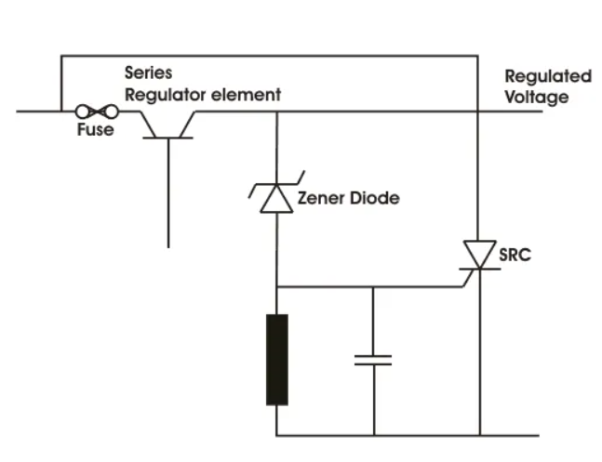
Fig 25. Overvoltage protection Circuit
As Voltage Regulator
This diode can be used to control the voltage in any circuit. There is constant output voltage at the output and it is driven by a current source. When voltage across the diode is more than certain value than excess current is drawn from the supply. To limit current a resistor is used whose value is calculated as

Fig 26. Zener Diode as Voltage Regulator
Resistor value = [(V1-V2)/ (Zener current + load current)]
As the regulating element connected in circuit is in parallel hence it is called as shunt regulator. The Zener diode produce a stable reference voltage across the load which fulfils the criterion of the regulator.
A junction diode which acts as a variable capacitor under changing reverse bias is known as a varactor diode.
We already studied that depletion layer is formed when p and n type material form pn junction diode. If there are no charge carriers within the depletion region, depletion region acts as an insulator.
The p-type material with holes as majority carriers and n-type material with elections as majority carriers act as charged plates. Thus the diode may be considered as a capacitor with n-region and p-region forming oppositely charged plates and with depletion region between them acting as a dielectric. Varactor diode is specially constructed to have high capacitance under reverse bias. The values of capacitance of varactor diodes are in the picofarad (1012 F) range.
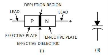
Figure 27: (i) Varactor diode (ii) Shows the symbol of varactor diode
A varactor diode is always reverse biased. The capacitance of varactor diode is given as:
Cγ = ε A/Wd
Where CT = Total capacitance of the junction
Ɛ = Permittivity of the semiconductor material
A = Cross-sectional area of the junction
Wd= Width of the depletion layer
When reverse voltage across a varactor diode is increased, the width Wd of the depletion layer increases. Therefore, the total junction capacitance CT of the junction decreases.
On the other hand, if the reverse voltage across the diode is decreased, the width Wd of the depletion layer decreases. Consequently, the total junction capacitance CT increases.
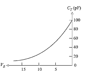
Figure 28: Shows the variation of VR and CT
Figure shows the variation of reverse bias varactor voltage VR and total junction capacitance CT. By changing varactor voltage VR we can easily change junction capacitance CT that is why varactor is also known as Voltage controlled capacitor.
Key Takeaways
- A junction diode which acts as a variable capacitor under changing reverse bias is known as a varactor diode.
- If there are no charge carriers within the depletion region, depletion region acts as an insulator.
- Varactor diode is specially constructed to have high capacitance under reverse bias. The values of capacitance of varactor diodes are in the picofarad (1012 F) range.
- The capacitance of varactor diode is given as:
CT = ε A/Wd
A scientist named Walter.H.Schottky first discovered Schottky diode. A Shockley diode is a PNPN device having two terminals. This device consists of four alternate P-type and N-type layers in a single crystal and acts as a switch. The various layers are labelled as P1, N1, P2, and N2 for identification.
Since a P-region adjacent to an N-region may be considered a junction diode, the Shockley diode is equivalent to three junction diodes connected in series as shown in Figure 37 (ii). The symbol of Shockley diode is shown in Figure 37 (iii).
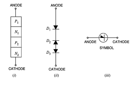
Figure 29: (i) Shockley diode (ii) equivalent figure to Shockley diode (iii)The symbol of Shockley diode
Schottky diode is a device, which comes under the type of a metal semiconductor junction diode. Barrier diode and low voltage diodes are the other names for Schottky diode. When compared to a PN junction diode, power drop is lower in Schottky diode.
Working
When we forward biased the Shockley diode i.e., making anode is more positive w.r.t. Cathode, as a result diodes D1 and D3 would be forward-biased while diode D2 would be reverse-biased. Since diode D2 offers very high resistance and the three diodes are in series, the Shockley diode presents a very high resistance. As the forward voltage increases, the reverse bias across D2 is also increased.
If we keep on increasing forward biasing a point reached when voltage become break over voltage VBO, reverse breakdown of D2 occurs. Since this breakdown results in reduced resistance, the Shockley diode presents a very low resistance. From now onwards, the Shockley diode behaves as a conventional forward-biased diode; the forward current being determined by the applied voltage and external load resistance.
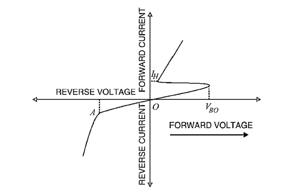
Figure 30: V-I characteristic
When Shockley diode is reverse biased (i.e., anode is negative w. Rt. Cathode), diodes D1 and D3 would be reverse-biased while diode D2 would be forward-biased. If reverse voltage is increased sufficiently, the reverse voltage breakdown (point A in Figure 36) of Shockley diode is reached. At this point, diodes D1 and D3 would go into reverse-voltage breakdown, the reverse current flowing through them would rise rapidly and the heat produced by this current flow could ruin the entire device. For this reason, Shockley diode should never be operated with a reverse voltage sufficient to reach the reverse-voltage breakdown point.
Shockley diode behaves like a switch. So long as the forward voltage is less than break over voltage, Shockley diode offers very high resistance (i.e. switch is open) and practically conducts no current. At voltages above the break-over value, Shockley diode presents a very low resistance (i.e. switch is closed) and Shockley diode conducts heavily.
It may be noted that Shockley diode is also known as PNPN diode or four layer diode or reverse-blocking diode thyristor.
Once Shockley diode is turned ON (i.e., it starts conducting), the only way to turn it OFF is to reduce the applied voltage to such a value so that current flowing through Shockley diode drops below its holding current IH value. Diode D2 then comes out of its reverse-breakdown state and its high-resistance value is restored. This, in turn, causes the entire Shockley diode to revert to its high-resistance (switch open) state.
Key Takeaways
- A Shockley diode is a PNPN device having two terminals.
- Shockley diode behaves like a switch.
- It may be noted that Shockley diode is also known as PNPN diode or four-layer diode or reverse-blocking diode thyristor.
- Once Shockley diode is turned ON (i.e., it starts conducting), the only way to turn it OFF is to reduce the applied voltage to such a value so that current flowing through Shockley diode drops below its holding current IH value.
The voltage regulators which are fabricated on a single silicon chip are called monolithic or IC regulators. Advantages of these regulators are small size, easy to use, high performance and low cost. Monolithic voltage regulators are three terminal devices having three terminals denoted as input, output and common terminals. These regulators are available in fixed or variable output voltage, positive or negative output voltage.
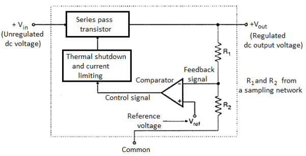
Fig 31. Block Diagram of 3-pin voltage regulator
Figure shows simplified block diagram of three pin regulator. The three terminals are Vin (input voltage), Vout (output voltage) and common terminal. The dc unregulated voltage is applied to the terminal Vin, supply ground to common and regulated output is taken at terminal Vout. The block diagram in fig. Above is basically a series regulator. The two resistors R1 and R2 form the sampling network to produce the feedback signal proportional to the output voltage. Vref is the internally generated voltage reference voltage.
This reference voltage is compared with the feedback signal by the comparator to produce the control voltage. This control signal is transferred through the thermal shutdown and current limiting block to the series pass transistor. The series pass transistor is operating as the control element. The voltage across the control element is varied by the control signal to get a constant output voltage. The thermal shutdown and current limiting block provide the protection against increased internal temperature or over current.
If the internal temperature exceeds a predetermined value, then the thermal shutdown block will not allow the control signal to pass through to the series pass transistor. This will turn off the chip automatically. The current limiting circuit protects the regulator against over current.
Three Terminal Fixed Voltage Regulators
The three terminal voltage regulators are of two types: Fixed and adjustable voltage regulators. In fixed voltage regulators we have positive voltage regulators and negative voltage regulators. The 78XX series is a series of fixed positive voltage regulators and the 79XX series is a series of fixed negative voltage regulators.
78XX Series: 78Xx series are three terminal, positive fixed voltage regulators. Here XX indicate the output voltage. These regulators are available in seven different output voltages such as 5, 6, 8, 12, 15, 18 and 24 volts. e.g. IC 7812 means +12V.
79XX Series: 79Xx series are three terminal, negative fixed voltage regulators. Here XX indicate the output voltage. These regulators are available in nine different output voltages such as 5, 6, 8, 12, 15, 18 and 24 volts in addition to this series provides -2 and -5.2V. e.g. IC 7812 means +12V.
A Positive 12 V Power supply using IC 7812: The circuit diagram of a 12 v regulated power supply using IC 7812is shown

The bridge rectifier and capacitor input filter produce an unregulated dc voltage which is applied at the Input terminal of IC 7812. As the minimum drop out voltage is 2v for Ic 7812, the voltage applied at the Input terminal should be at least 14V. C1 is the filter capacitor and C2 is connected at the output terminal to improve the transient response of the regulator.
LED or Light emitting diode
Light emitting diode is a pn junction device. It is always operated in forward biased condition. LED converts electrical energy into light energy.

Figure 32: LED
Device Structure:
The LED structure plays a crucial role in emitting light from the LED surface. The LEDs are structured to ensure most of the recombination takes place on the surface by the following two ways.
- By increasing the doping concentration of the substrate, so that additional free minority charge carrier’s electrons move to the top, recombine and emit light at the surface.
- By increasing the diffusion length L =√Dτ, where D is the diffusion coefficient and τ is the carrier life time.
But when increased beyond a critical length there is a chance of reabsorption of the photons into the device. The LED has to be structured so that the photons generated from the device are emitted without being reabsorbed.
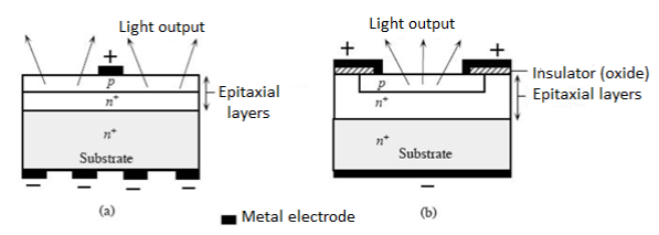
Figure 33: A schematic illustration of typical planar surface emitting LED devices. (a) p-layer grown epitaxially on an n+ substrate. (b) First n+ is epitaxially grown and then p region is formed by dopant diffusion into the epitaxial layer.
One solution is to make the p layer on the top thin, enough to create a depletion layer. Following picture shows the layered structure. There are different ways to structure the dome for efficient emitting
LEDs are usually built on an n-type substrate, with an electrode attached to the p-type layer deposited on its surface. P-type substrates, while less common, occur as well. Many commercial LEDs, especially GaN/InGaN, also use sapphire substrate.
In the fabrication of LED’s direct band gap semiconductors like GaP, GaAsP are used. In direct band gap semiconductor most of the energy is emitted in the form of light when hole and electron recombination takes place.
When an LED is forward biased the electrons and holes move in towards the junction and recombination takes place. As a result of recombination the electrons lying in the conduction band of an n- region fall into the holes lying in the valence band of a p –region. The difference of energy in the valence band and conduction band is radiated in the form of light energy. Here their excess energy is transferred to the emitted photon. The brightness of emitted light is directly proportional to the forward bias current.
Figures of Merit
A very important metric of an LED is the external quantum efficiency ηext. It quantifies the efficiency of the conversion of electrical energy into emitted optical energy.
Not all the photons emitted from the active region of an LED make it out of the device. Some are reabsorbed, some go in the wrong direction, some are reflected back. The light extraction efficiency of a LED is,
ηextraction 
The external quantum efficiency ext of a LED is,
ηextraction 
It is defined as the light output divided by the electrical input power. It is also defined as the product of Internal radiative efficiency and Extraction efficiency. ηext = Pout(optical)/ IV
For indirect bandgap semiconductors ηext is generally less than 1%, whereas for a direct band gap material it could be substantial.
ηint = rate of radiation recombination/ Total recombination
The internal efficiency is a function of the quality of the material and the structure and composition of the layer.
LED materials
LEDs are comprised of compound semiconductor materials, which are made up of elements from group III and group V of the periodic table (these are known as III-V materials). Examples of III-V materials commonly used to make LEDs are gallium arsenide (GaAs) and gallium phosphide (GaP).
Ternary alloys based on alloying GaAs and GaP which are denoted by GaAs1-yPy. Inga Alp is an example of a quaternary (four elements) III-V alloy with a direct band gap. The LEDs realized using two differently doped semiconductors that are the same material is called a homojunction. When they are realized using different bandgap materials they are called a heterostructure device. A heterostructure LED is brighter than a homoJunction LED.
The main semiconductor materials used to manufacture LEDs are:
- Indium gallium nitride (InGaN): blue, green and ultraviolet high-brightness LEDs
- Aluminium gallium indium phosphide (AlGaInP): yellow, orange and red high-brightness LEDs
- Aluminium gallium arsenide (AlGaAs): red and infrared LEDs
- Gallium phosphide (GaP): yellow and green LEDs
Characteristics of LED
LEDs are solid-state devices. The advantages are:
1) Light Generated by LED is Directional
2) LED can Generate Different Light Colour
3) Temperature will Affect LED Efficacy
4) Low Energy Consumption
5) Long Life
The usage of LED is advantageous as it consumes less power and produces less heat. LEDs last longer than incandescent lamps.
Applications LEDs are used in
- For instrument display
- In calculators
- Digital clocks
- For indicating power ON/ OFF
- For optical switching application
- In optical communication system
- Medical devices
Key Takeaways
- Light emitting diode is a pn junction device. It is always operated in forward biased condition. LED converts electrical energy into light energy.
- When an LED is forward biased the electrons and holes move in towards the junction and recombination takes place.
- The light extraction efficiency of a LED is,
ηextraction 
- LEDs are comprised of compound semiconductor materials, which are made up of elements from group III and group V of the periodic table (these are known as III-V materials). Examples of III-V materials commonly used to make LEDs are gallium arsenide (GaAs) and gallium phosphide (GaP).
The photodiode is a p-n junction semiconductor diode which is always operated in the reverse biased condition.
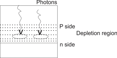
The light is always focused through a glass lens on the junction of the photodiode As the photodiode is reverse biased the depletion region is quite wide, penetrated on both side of the junction.
The photons incident on the depletion region will impact their energy to the Ions present in depletion region and generates e hole pairs.
The photons incident on the depletion region so the number of electron hole pairs will be generated depends on the intensity of light [number of photons] These and holes will be attracted towards the +ve& -ve terminals respectively of the photo current,
With increase in the light intensity a greater number of e hole pairs are generated and the photo current increases thus the photocurrent is proportional to the light intensity.
Bipolar junction transistor or BJT is simply known as Transistor. A transistor consists of two pn junctions formed by sandwiching either p-type or n-type semiconductor between a pair of opposite types.
The prefix 'trans' means the signal transfer property of the device while 'istor ' classifies it as a solid element in the same general family with resistors. Accordingly, there are two types of transistors
- n-p-n transistor
- p-n-p transistor
An n-p-n transistor is composed of two n-type semiconductors separated by a thin section of p-type as shown in Figure 1 (i).
However, a p-n-p transistor is formed by two p-sections separated by a thin section of n-type as shown in Figure 1(ii).

Figure 34: (i) n-p-n transistor (ii) p-n-p transistor
In each type of transistor, the following points may be noted:
- Transistor may be regarded as a combination of two diodes connected back to back.
- There are three terminals, one taken from each type of semiconductor.
- The middle section is a very thin layer. The thin layer plays an important role in the function of a transistor.
A transistor has two pn junctions. One junction is forward biased and the other is reverse biased. The forward biased junction has a low resistance path whereas a reverse biased junction has a high resistance path. The weak signal is introduced in the low resistance circuit and output is taken from the high resistance circuit. Therefore, a transistor transfers a signal from a low resistance to high resistance.
A transistor (pnp or npn) has three sections of doped semiconductors. The section on one side is the emitter and the section on the opposite side is the collector. The middle section is called the base and forms two junctions between the emitter and collector.

Figure 35: (i) p-n-p transistor (ii) n-p-n transistor
Emitter: The section on one side that supplies charge carriers (electrons or holes) is called the emitter. The emitter is always forward biased w.r.t. Base so that it can supply a large number of majority carriers. In Figure 2 (i), the emitter (p-type) of pnp transistor is forward biased and supplies hole charges to its junction with the base. Similarly, in Figure 2 (ii), the emitter (n-type) of npn transistor has a forward bias and supplies free electrons to its junction with the base.
Collector: The section on the other side that collects the charges is called the collector. The collector is always reverse biased. Its function is to remove charges from its junction with the base. In Figure 2 (i), the collector (p-type) of pnp transistor has a reverse bias and receives hole charges that flow in the output circuit. Similarly, In Figure (ii), the collector (n-type) of npn transistor has reverse bias and receives electrons.
Base: The middle section which forms two pn junctions between the emitter and collector is called the base. The base emitter junction is forward biased allowing low resistance for the emitter circuit. The base-collector junction is reverse biased and provides high resistance in the collector circuit.
Before studying action of transistor, some important facts about transistor should be keep in mind.
- The transistor has two pn junctions i.e. it is like two diodes. The junction between emitter and base may be called emitter-base diode or simply the emitter diode. The junction between the base and collector may be called collector-base diode or simply collector diode.
- The emitter diode is always forward biased whereas collector diode is always reverse biased.
- Three regions of transistor are emitter, base and collector. The base is much thin as compared to emitter while "collector is wider than both. To keep it simple it is assumed emitter and collector is considered to be of same size.
- The emitter is heavily doped so that it can inject a large number of charge carriers (electrons or holes) into the base. The base is lightly doped and very thin it passes most of the emitter injected charge carriers to the collector. The collector is moderately doped.
- The resistance of emitter diode (forward biased) is very small as compared to collector diode (reverse biased). Therefore, forward bias applied to the emitter diode is generally very small whereas reverse bias on the collector diode is much higher.
Working of Transistor
(i) Working of npn transistor: As discussed in the npn transistor emitter-base junction is forward biased to emitter-base junction and collector-base junction is reverse biased. The forward bias causes the electrons in the n-type emitter to flow towards the base. This constitutes the emitter current Ie.
Ie =Ib + Ic
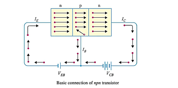
Figure 36: n-p-n transistor
As these electrons flow through the p-type base, they tend to combine with holes. As the base is lightly doped and very thin, therefore, only a few electrons (less than 5%) combine with holes to constitute base current Ib. The remainder i.e. more than 95% cross over into the collector region to constitute collector current Ic In this way, almost the entire emitter current flows in the collector circuit. It is clear that emitter current is the sum of collector and base currents i.e.
(ii) Working of pnp transistor: In the pnp transistor emitter-base junction is forward biased to emitter-base junction and collector-base junction is reverse biased. The forward bias causes the holes in the p-type emitter to flow towards the base. This constitutes the emitter current Ie. As these holes cross into n-type base, they tend to combine with the electrons. As the base is lightly doped and very thin, therefore, only a few holes (less than 5%) combine with the electrons.

Figure 37: p-n-p transistor
The remainder (more than 95%) cross into the collector region to constitute collector current Ic. In this way, almost the entire emitter current flows in the collector circuit. It may be noted that current conduction within pnp transistor is by holes. However, in the external connecting wires the current is still by electrons.
Thus the input circuit (i.e. emitter-base junction) has low resistance because of forward bias whereas output circuit (i.e. collector base junction) has high resistance due to reverse bias. As we have seen, the input emitter current almost entirely flows in the collector circuit. Therefore a transistor transfers the input signal current from a low resistance circuit to a high-resistance circuit.
Transistor’s Configuration:-
1) Common Base configuration(C.B)
2) Common emitter Configuration(C.E)
3) Common Collector Configuration(C.C)
COMMON BASE CONFIGURATION
- The notation and symbols of pnp and npn transistors are given below:
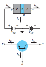
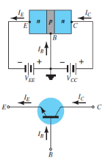
Figure 38: PNP CB and NPN CB
- Here the base is common to both the input and output sides of the configuration.
- The flow of holes will govern the direction of current.
- Hence, Ic = Ib + Ie
Where Ic, Ib, Ie are the collector, base and emitter currents respectively.
- The graphical symbol of the PNP common base configuration is
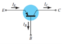
Figure 39: PNP common base
- The arrow in the above symbol shows the direction of emitter current in the device.
- Now, to study the behavior of the device we require two characteristics:
Input Characteristic Curve
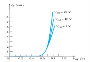
Figure 40: Input Characteristic Curve
- It is the relation between the input current IE to the input voltage VBE for various levels of output voltage VCB.
- It is also known as driving point characteristics.
Output Characteristic Curve
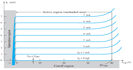
Figure 41: Output Characteristic Curve
- It is the relation between the output current IC to the output voltage VCB for various levels of input current IE.
- It is also known as collector set of characteristics.
- It has three basic regions:
- Active Region
- Here, base-emitter junction is forward biased and collector-base junction is reverse biased.
- As input current IE increases above zero, output current IC increases to a magnitude equal to IE as determined by the basic transistor current relationship.
- So the first approximation determined by the curve is
IC ≈ IE
2. Cut-off Region
- It is defined as the region where the collector current IC is equal to 0A.
- Here, the base-emitter junction and the collector-base junction both are in reverse bias.
3. Saturation Region
- It is the region that lies towards the left of VCB = 0V.
- Here, the base-emitter junction and the collector-base junction both are in forward bias.
COMMON EMITTER CONFIGURATION
- The notation and symbols of npn and pnp transistors are given below:
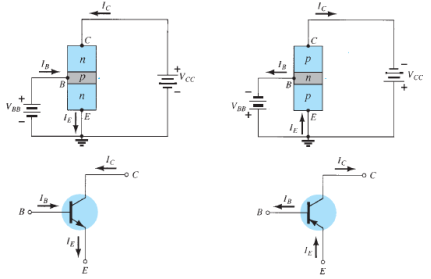
Figure 42: NPN CE and PNP CE
- In the above figure all the currents are shown in their actual conventional directions.
- The current relation developed earlier is still applicable,
IE = IB + IC
Where IE , IB , IC are the collector, base and emitter currents respectively.
- The graphical symbol of the PNP common emitter configuration is
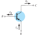
Figure 43: PNP common emitter (Ref. 2)
- Now, to study the behavior of the device we require two characteristics:
Input Characteristic Curve
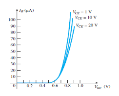
Figure 44: Input Characteristic Curve (Ref. 2)
- It is the graph between the input current IB to the input voltage VBE for a range of values of output voltage VCE.
- Note that the magnitude IB of is in micro amperes and that of IC is in milli amperes.
Output Characteristic Curve
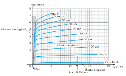
Figure 45: Output Characteristic Curve
- It is the graph between the output current IC to the output voltage VCE for a range of values of input current IB.
- It has three basic regions:
Active Region
- Here, the base-emitter junction is forward biased and collector base junction is reverse biased.
- These are the same conditions that existed in the active region of the common base configuration.
- This can be employed for voltage, current or power amplification.
Cut-off Region
- Here IC is not equal to zero when IB is zero.
- For linear amplification purposes, it is defined as IC = ICEO .
- The region below IB = 0µA is to be avoided for undistorted output signal.
- When the transistor is used as a switch, the condition should be ideally IC = 0mA for a chosen VCE voltage.
Saturation Region
- It is the region that lies towards the left of VCE = 0V.
COMMON COLLECTOR CONFIGURATION
- The notation and symbols of npn and pnp transistors are given below:

Figure 46: NPN CC and PNP CC (Ref. 2)
- In the above figure all the currents are shown in their actual conventional directions.
- It is used for impedence matching purposes as it has high input impedence and low output impedence.
- It can be designed using common emitter characteristics.
- The output characteristics of common collector is same as that of common emitter configuration for all practical purposes.
- The output characteristics are a plot between IE versus VCE for all values of IB.
- The input current of common collector is same as that of common emitter configuration.
- Here the region of operation will ensure that maximum ratings are not being exceeded and output ratings have minimum distortion.
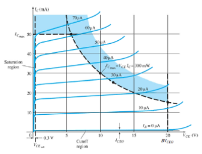
Figure 47: Output Characteristic Curve (Ref. 2)
- The characteristics specifying the minimum VCE that can be applied without entering the non-linear region is saturation region.
- The maximum power dissipation is given by,
P = VCE . IC
Key Takeaways
- A transistor consists of two pn junctions formed by sandwiching either p-type or n-type semiconductor between a pair of opposite types.
- There are two types of transistors n-p-n transistor and p-n-p transistor.
- The emitter diode is always forward biased whereas collector diode is always reverse biased.
- Three regions of transistor are emitter, base and collector. The base is much thin as compared to emitter while "collector is wider than both. To keep it simple it is assumed emitter and collector is considered to be of same size.
- The emitter is heavily doped so that it can inject a large number of charge carriers (electrons or holes) into the base. The base is lightly doped and very thin it passes most of the emitter injected charge carriers to the collector. The collector is moderately doped.
- Transistor’s Configuration:-Common Base configuration(C.B), Common emitter Configuration(C.E), Common Collector Configuration(C.C)
Comparison of all configuration
Sr.no | Parameter | CB | CE | CC |
1 | Common terminal between I/p & o/p | Base | Emitter | Collector |
2 | Input Current | IE | IB | IB |
3 | Output Current | IC | IC | IE |
4 | Current Gain |   |   | ɤ=   |
5 | Input Voltage. | VEB | VBE | VBC |
6 | Output Voltage. | VCB | VCE | VCC |
Comparison of all Modes
Parameters | Common-Emitter (CE) Amplifier | Common-Base (CB) Amplifier | Common-Collector (CC) Amplifier |
Input resistance | Moderate βre | Low re | High βRE |
Output resistance | High RC | High RC | Low re |
Voltage gain | High rL/re | High rL/re | About 1 |
Current gain | High β | Low, about 1 | High (1 + β) |
Power gain | High | Moderate | Low |
Phase shift | 180o | 0o | 0o |
BJT as a switch
Suppose we had a lamp that we wanted to turn on and off with a switch. Such a circuit would be extremely simple, as in the figure below.

a- mechanical switch
b- NPN transistor switch
c- PNP transistor switch
Figure 48. Transistor as switch
Suppose we insert a transistor in place of the switch to show how it can control the flow of electrons through the lamp. Remember that the controlled current through a transistor must go between collector and emitter.

Figure 49. Transistor: a) cut-off lamp b) saturated, lamp on.
The choice between NPN and PNP is really arbitrary. All that matters is that the proper current directions are maintained for the sake of correct junction biasing.
In the above figures, the base of either BJT is not connected to a suitable voltage, and no current is flowing through the base. Consequently, the transistor cannot turn on. Therefore, connect a switch between the base and collector wires of the transistor as in figure.
If the switch is open as in figure (a), the base wire of the transistor will be left “floating” and there will be no current through it. In this state, the transistor is said to be cut-off.
If the switch is closed as in figure (b), current will be able to flow from the base to the emitter of the transistor through the switch. This base current will enable a much larger current flow from the collector to the emitter, thus lighting up the lamp. In this state of maximum circuit current, the transistor is said to be saturated.
BJT as an Amplifier
Transistor raises the strength of a weak signal and hence acts an amplifier. The transistor amplifier circuit is shown in the figure below.
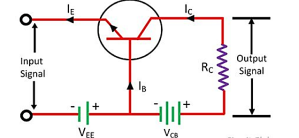
Figure 50. Transistor as an Amplifier
The transistor has three terminals namely emitter, base and collector. The emitter and base of the transistor are connected in forward biased and the collector base region is in reverse bias. The forward bias means the P-region of the transistor is connected to the positive terminal of the supply and the negative region is connected to the N-terminal and in reverse bias just opposite of it has occurred.
Vee is applied to the input circuit along with the input signal to achieve the amplification. The DC voltage VEE keeps the emitter-base junction under the forward biased condition regardless of the polarity of the input signal and is known as bias voltage.
When a weak signal is applied to the input, a small change in signal voltage causes a change in emitter current this change is almost the same in collector current because of the transmitter action.
In the collector circuit, a load resistor RC of high value is connected. When collector current flows through such a high resistance, it produces a large voltage drop across it. Thus, a weak signal (0.1V) applied to the input circuit appears in the amplified form (10V) in the collector circuit.
Input Resistance
When the input circuit is forward biased, the input resistance will be low. The input resistance is the opposition offered by the base-emitter junction to the signal flow.
Hence, it is the ratio of small change in base-emitter voltage (ΔVBE) to the resulting change in base current (ΔIB) at constant collector-emitter voltage.
Input resistance, Ri=ΔVBE/ΔIb
Where Ri = input resistance, VBE = base-emitter voltage, and IB = base current.
Output Resistance
The output resistance of a transistor amplifier is very high. The collector current changes very slightly with the change in collector-emitter voltage.
The ratio of change in collector-emitter voltage (ΔVCE) to the resulting change in collector current (ΔIC) at constant base current.
Output resistance = Ro=ΔVCE/ΔIC
Where Ro = Output resistance, VCE = Collector-emitter voltage, and IC = Collector-emitter voltage.
Current gain
It is the ratio of change in collector current (ΔIC) to the change in base current (ΔIB).
Current gain, β=ΔIC/ ΔIB
Voltage Gain
It is the ratio of change in output voltage (ΔVCE) to the change in input voltage (ΔVBE).
Voltage gain, AV=ΔVCE/ΔVBE

Power Gain
It is the ratio of output signal power to the input signal power.
Power gain, Ap = 

= current gain x voltage gain
Construction
- An FET is a three-terminal amplifying device.
- Its terminals are source, gate, and drain, which acts respectively like emitter, base, and collector of a normal transistor.
- There are two distinct families of FETs.
- The first is known as ‘junction-gate’ types of FETs or JUGFET or JFET.
- The second family is called ‘insulated-gate’ FETs or Metal Oxide Semiconductor FETs or MOSFET.
- ‘N-channel’ and ‘p-channel’ are the two versions of both types of FET.
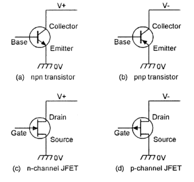
Working
- N-channel FET consists of n-type semiconductor material with a drain terminal and a source terminal at opposite ends.
- A p-type gate is joined in the middle section of the n-type bar, thus forming a p-n junction.
- The drain terminal is connected to a positive supply and the gate is biased at a value that is negative (or equal) to the source voltage, thus reverse-biasing the JFET’s internal p-n junction, and accounting for its very high input impedance.
- When gate = 0V, a current flow from drain to source via a conductive ‘channel’ and the n-type bar is formed.
- When gate = negative , a high resistance region is formed within the junction, thus reduces the magnitude of the drain-to-source current and width of the n-type conduction channel.
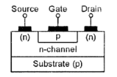
- Thus, the basic JFET passes maximum current when its gate bias is zero, and its current is reduced or ‘depleted’ when the gate bias is increased. It is thus known as a ‘depletion-type’ n-channel JFET.
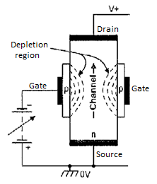
JFET parameters
1. Gate Cut Off Voltage
At a fixed drain voltage, the drain current (ID) of a JFET depends on the gate to source voltage (VGS). If the gate to source voltage decreases in n channel JFET, the drain current also gets decreased accordingly.
The relation between gate to source voltage and drain current is given by
ID = IDSS 
2. Shorted Gate Drain Current
When (VGS = 0) and positive drain to source voltage (VDS) is being increased slowly, the drain current gets increased linearly. But after pinch-off voltage (Vp), the drain current increases and gets a constant value. This is the maximum drain current that flows through the channel and is called shorted gated drain current and denoted by IDSS.
3. Transconductance
Transconductance is defined as the ratio of change in drain current (δID) to change in the gate to source voltage (δVGS) with a constant drain to source voltage (VDS = Constant).
gm = δTD/δVGS at constant VDS
4. Dynamic Output Resistance
It is the ratio of change of drain to source voltage (δVDS) to the change of drain current (δID) keeping a constant gate to source voltage (VGS = Constant). The ratio is denoted as rd.
rd = δVDS/δID at constant VGS
5. Amplification Factor
It is defined as the ratio of change of drain voltage (δVDS) to change of gate voltage (δVGS) at a constant drain current (ID = Constant).
μ = δVDS/δVGS atconstant ID
There is a relation between transconductance (gm) and dynamic output resistance (rd) and is given as.
μ = δVDS/δVGS = δVDS/δID δID/δVGS
μ = rd gm
JFET characteristics
There are two types of static characteristics viz
(1) Output or drain characteristic
(a) Drain Characteristic with Shorted-Gate
- The curve drawn between drain current Ip and drain to source voltage VDS with gate to source voltage VGS as the parameter is called the drain or output characteristic.
- When Vns = zero, there is no potential at the drain, therefore no current flows.
- Hence drain current ID = 0.
- For small voltage Vna, the N-type bar acts as a semiconductor resistor, and the drain current increases linearly with the increase in Vds.
- The region present to the left of the knee point is called the channel ohmic region, as in this region the FET behaves like an ordinary resistor.
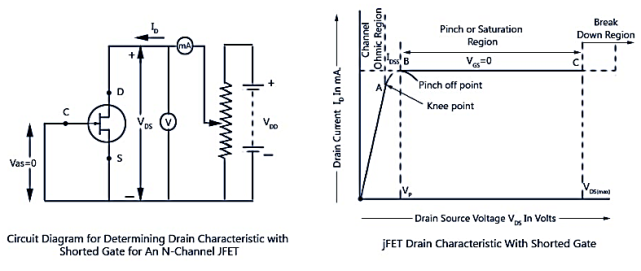
(b) Drain Characteristics With External Bias
Here, the circuit diagram determines the drain characteristics with different values of external bias and a family of drain characteristics for different values of gate-source voltage VGS.

As the negative gate bias voltage increases:
(1) The maximum saturation drain current becomes smaller because the conducting channel becomes narrower.
(2) Pinch-off voltage reaches at a lower value when VGS = 0.
(3) The ohmic region portion decreases.
(4) The value of drain to source voltage VDS for the avalanche breakdown of the gate junction is reduced.
Hence, in the pinch-off or active region it is necessary to satisfy the following conditions:
VP < VDS < VDS (max)
VGS (OFF)< VGS < 0
0 < ID < IDSS
(2) Transfer characteristic.
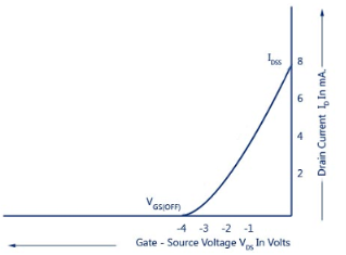
It is determined by experimentally keeping drain to source voltage, VDS constant and determining drain current, ID for various values of gate-source voltage, VGS. The curve is plotted between gate to source voltage, VGS and drain current, ID. It is observed that
(i) ID decreases with the increase in negative gate to source voltage
(ii) ID = IDSS when VGS = 0
(iii) ID = 0 when VGS = VD
Key takeaway
S.No. | JFET | MOSFET |
1 | Operated in depletion mode | Operated in depletion mode and enhancement mode |
2 | High input impedance(>10MΩ) | Very High input impedance (>10000 MΩ) |
3 | Gate is not insulated from channel | Gate is insulated from channel by a layer of Sio2 |
4 | Channel exists permanently | Channel exists permanently in depletion type but not in enhancement type |
5 | Difficult to fabricate than MOSEFT | Easier to fabricate |
6 | Drain resistance is high | Drain resistance is less |
7 | Gate is formed as a diode | Gate is formed as a capacitor |
MOSFETs are three terminal devices with a Gate, Drain and Source and both P-channel (PMOS) and N-channel (NMOS) MOSFETs are available. The main difference this time is that MOSFETs are available in two basic forms:
- Depletion Type – the transistor requires the Gate-Source voltage, ( VGS ) to switch the device “OFF”. The depletion mode MOSFET is equivalent to a “Normally Closed” switch.
- Enhancement Type – the transistor requires a Gate-Source voltage, ( VGS ) to switch the device “ON”. The enhancement mode MOSFET is equivalent to a “Normally Open” switch.
The symbols and basic construction for both configurations of MOSFETs are shown below.
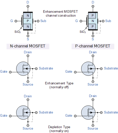
The four MOSFET symbols above show an additional terminal called the substrate and is not normally used as either an input or an output connection but instead it is used for grounding the substrate. It connects to the main semiconductive channel through a diode junction to the body or metal tab of the MOSFET.
The line in the MOSFET symbol between the drain (D) and source (S) connections represents the transistors semiconductive channel. If this channel line is a solid unbroken line then it represents a “Depletion” (normally-ON) type MOSFET as drain current can flow with zero gate biasing potential.
If the channel line is shown as a dotted or broken line, then it represents an “Enhancement” (normally-OFF) type MOSFET as zero drain current flows with zero gate potential. The direction of the arrow pointing to this channel line indicates whether the conductive channel is a P-type or an N-type semiconductor device.
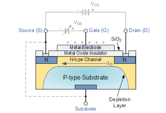
The construction of the Metal Oxide Semiconductor FET is different to that of the Junction FET.
Both the Depletion and Enhancement type MOSFETs use an electrical field produced by a gate voltage to alter the flow of charge carriers, electrons for n-channel or holes for P-channel, through the semi-conductive drain-source channel.
The gate electrode is placed on top of a very thin insulating layer and there are a pair of small n-type regions just under the drain and source electrodes.
With the insulated gate MOSFET device no such limitations apply so it is possible to bias the gate of a MOSFET in either polarity, positive (+ve) or negative (-ve).
This makes the MOSFET device especially valuable as electronic switches or to make logic gates because with no bias they are normally non-conducting and this high gate input resistance means that very little or no control current is needed as MOSFETs are voltage controlled devices.
Both the p-channel and the n-channel MOSFETs are available in two basic forms, the Enhancement type and the Depletion type.
MOSFET is another type of field effect transistor. The MOSFET has become one of the most important devices used in design and construction computers
MOSFET [metal oxide semiconductor field effect transistor]
Type of MOSFET
- Depletion type MOSFET
- Enhancement type MOSFET
- Power MOSFET
Enhancement type MOSFET: classified in to two type n. Channel or p. Channel E MOSFET
A) N-channel E MOSFET
B) P-channel E MOSFET
N-channel E MOSFET
Figure 51: N-channel E MOSFET
- A slab of P-type semiconductor is used as substrate. The substrate is sometimes connected to the source otherwise it is brought out as the fourth terminal.
- The drain and source terminal are connected to the n-type doped regions through the metallic contacts.
- The insulating sio2 layer is still present which isolates gate terminal from the substrate.
Effect of the insulting sio2 layer:
Due to the presence of the sio2 layer between gate terminal and n-type channel the i/p impedance of MOSFET is very high this is a desirable fracture of a MOSFET. Due to high i/p impedance the gate current IG= 0 for the d.c operating conditions.
Operation: the operation can be explained with two different operating
- Operation with VGS = 0
- Operation when VGS is +ve
1) Operating with VGS = 0 Volt
If VGS = 0 and a positive voltage is applied between its drain and source, then due to the absence of the n-type channel a zero drain current will result.
2) Operation when Vgs Positive:
The positive potential at the gate terminal will repel the holes present in the p-type substrate.
Figure 52: Operation on N-channel E MOSFET
Formation of induced channel in n-channel enhancement MOSFET
This creates a depletion region near the sio2 insulating layer. But the minority carriers ie the electrons in the p-type substrate will be attracted towards the gate terminal and gather near the surface of sio2 as shown above
As we increase the positive VGS the number of e- gathering near the sio2 layer increases to such an extent that it creates an induced n-channel which connects the n-type doped regions.
The drain current then starts flowing through this induced channel. The value of VGS at which this conduction begins is called as the threshold Vtg. & is indicated.
V-I Characteristics
Characteristics of n-channel enhancement type MOSFET:

Transfer characteristics drain characteristics
Figure 53: Characteristics of n-channel enhancement type MOSFET
P-channel enhancement type MOSFETS:
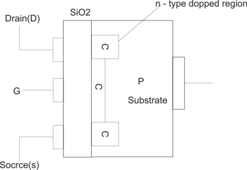
Figure 54: P-channel enhancement type MOSFETS
The construction of p-channel EMOSFET is exactly opposite to that of a n-channel EMOSFET.
Characteristics:
Drain Characteristics of transfer Characteristics of p-channel E MOSFET
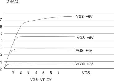
Figure 55: Characteristics of p-channel enhancement type MOSFET
Regions Of Operation, MOSFET As Switch & Amplifier
Operation: the operation can be explained with two different operating
Operation with VGS = 0
Operation when VGS is +ve
Operating with VGS = 0 Volt
If VGS = 0 and a positive voltage is applied between its drain and source, then due to the absence of the n-type channel a zero drain current will result.
Operation when Vgs Positive:
The positive potential at the gate terminal will repel the holes present in the p-type substrate.
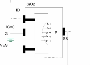
Figure 56: Formation of induced channel in n-channel enhancement MOSFET
Formation of induced channel in n-channel enhancement MOSFET
- This creates a depletion region near the sio2 insulating layer. But the minority carriers ie the electrons in the p-type substrate will be attracted towards the gate terminal and gather near the surface of sio2 as shown above
- As we increase the positive VGS the number of e- gathering near the sio2 layer increasesto such an extent that it creates an induced n-channel which connects the n-type doped regions.
- The drain current then starts flowing through this induced channel. The value of VGS at which this conduction begins is called as the threshold Vtg. & is indicated
Effect of increase in the drain to source Vtg.:
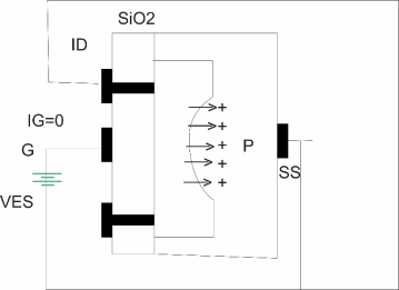
Figure 57: Effect of increase in the drain to source Vtg:
Effect of changes in VDS at fixed VGS on the channel width:
- The positive gate to source voltage VDS is kept constant and the drain to source voltage VGS is increased gradually.
- Due to this the gate terminal becomes less and less positive with respect to the drain so less number of electron are attracted towards gate terminal & the induced channel becomes narrow.
- Eventually the channel width will be reduced to a point of pinch off and the saturation condition will be established which is same as that in a JFET
- That means any further increase in VDS at the fixed value of VGS will not affect the saturation level of ID unless breakdown condition are encountered.
Symbols:
1) N-channel EMOSFET
2) P-channel EMOSFEJ
BJT is a bipolar device [minority & majority carriers both contributes to the current flow]
E MOSFET is a unipolar device ie current flows only due to the majority carriers
BJT thermal runaway can damage BJT thermal runway does not take place.
BJT low i/p impedance, E MOSFET High i/p impedance
- Voltage ampɤ
- Current and vtg gain
Current gain AI is defined as the ratio of o/p current
AI = Io/Ii
Vtg gain is given by
Av = Vo/V
Av = RL/(Ro + RL) Avi/Vi
Av = A RL/(Ro + RL)
In this expression if Ro is very small as compared to RL then Av A
A
Thus we can say that the overall gain of the ampere Av will approach its open circuit value A if Ro << RL
Problem: An amplifier has a signal i/p Vtg. Vi of 0.25v and draws 1mA from the source. The amɤ delivers & v to a load at 10 mA. Determine the current Vtg and power gains. Also find the i/p resistance of this ampɤ what must be the open ckt. Vtg of the source Vs to provide an ampɤ i/p VtgVi of 0.25 v when the internal resistance of the source is 50 Ω?
Given Vi = 0.25v, Ii = 1 Ma, Vo = 8 v, Io = 10 mA, Rs = 50 Ω.
Solution:
Vtg gain Av = Vo/Vi = 8/0.25 = 32
Current gain Al = Io/Ii = 10m/1m
Power gain AP = Av A1 = 32 10 = 320
Input resistance Ri = Vi/Ri = 0.25/1 10-3 = 250
Open circuit Vtg of Vs
Vi = Ri/(Ri + Rs) Vs
Vs = (Ri + Rs)/Ri Vi
Vs = (250 + 50)/250 0.25
Vs = 0.3v
MOSFET as switch:
- MOSFET can act as a switch jest like a transistor a typical switching Ckt using N-channel EMOSFET shown below
- A positive going i/p pulse (high i/p) turns on the EMOSFET. Maxm drain current flows and the o/p Vtg drops from +VDD to RD ID (on). So the EMOSFET acts as closed switch.
- Similarly when the i/p is low (zero) no drain current and hence the o/p is equal to +VDD. So the EMOSFET acts as open s/w
EMOSFET as an AMP:
The purpose of amplifier is to amplify the weak signal faithfully. For amplification MOSFET should operate in a saturation region.
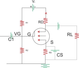
Figure 58: EMOSFET as an AMP
N-channel E-MOSFET Ampɤ
- It can operate with positive gate and drain Vtg where as in p-channel with –ve gate and drain Vtg
- For amplification MOSFET should operate in saturation region where the drain current ID remains constant
- The threshold Vtg (VT) is the minimum gate Vtg (VGS) required to induce the channel between source to drain
- Fig shows single stage common source ampɤ using Vtg bias method
- Vin is A.c. Signal
- Resistors R1 ,R2 and R5 provides the proper and stabilized operating point
- C in i/p coupling capacitor where is coat is the o/p coupling capacitor which blocks the d.c signal
- Cs is the bypass capacitor so that signal available at source terminal. Never pass through Rs otherwise o/p Vtg reduces.
Key Takeaways
- MOSFET is another type of field effect transistor. The MOSFET has become one of the most important devices used in design and construction computers
- MOSFET [metal oxide semiconductor field effect transistor]
- Type of MOSFET are Depletion type MOSFET, Enhancement type MOSFET and Power MOSFET
- Enhancement type MOSFET: classified in to two type n. Channel or p. Channel E MOSFET
- The operation can be explained with two different operating; Operation with VGS = 0 and Operation when VGS is +ve
- Vtg gain is given by Av = RL/(Ro + RL) Avi/Vi
- MOSFET can act as a switch jest like a transistor a typical switching.
References:
1. Integrated Devices & Circuits by Millman & Halkias, TMH Publications.
2. Electronics Devices and Circuit Theory by R. Boylestad & L. Nashelsky, Pearson Publication
3. Electronic Communication System by G. Kennedy, TMH Publications.
4. Basic Electronics by Sanjeev Kumar & Vandana Sachdeva, Paragaon International Publication