Unit - 3
Digital Electronics Fundamentals
Analog | Digital |
An analog signal is a continuous signal that represents physical measurements. | Digital signals are time separated signals which are generated using digital modulation. |
It is denoted by sine waves | It is denoted by square waves |
It uses a continuous range of values that help you to represent information. | Digital signal uses discrete 0 and 1 to represent information. |
Temperature sensors, FM radio signals, Photocells, Light sensor, Resistive touch screen are examples of Analog signals. | Computers, CDs, DVDs are some examples of Digital signal. |
The analog signal bandwidth is low | The digital signal bandwidth is high. |
Analog signals are deteriorated by noise throughout transmission as well as write/read cycle. | Relatively a noise-immune system without deterioration during the transmission process and write/read cycle. |
Analog hardware never offers flexible implementation. | Digital hardware offers flexibility in implementation. |
It is suited for audio and video transmission. | It is suited for Computing and digital electronics. |
Processing can be done in real-time and consumes lesser bandwidth compared to a digital signal. | It never gives a guarantee that digital signal processing can be performed in real time. |
Analog instruments usually have s scale which is cramped at lower end and gives considerable observational errors. | Digital instruments never cause any kind of observational errors. |
Analog signal doesn't offer any fixed range. | Digital signal has a finite number, i.e., 0 and 1. |
Boolean Algebra is used to analyze and simplify the digital (logic) circuits. It uses only the binary numbers i.e. 0 and 1. It is also called as Binary Algebra or logical Algebra. Boolean algebra was invented by George Boole in 1854.
Rule in Boolean Algebra
Following are the important rules used in Boolean algebra.
- Variable used can have only two values. Binary 1 for HIGH and Binary 0 for LOW.
- Complement of a variable is represented by an overbar (-). Thus, complement of variable B is represented as
 . Thus if B = 0 then
  = 1 and B = 1 then
  = 0.
= 0. - ORing of the variables is represented by a plus (+) sign between them. For example ORing of A, B, C is represented as A + B + C.
- Logical ANDing of the two or more variable is represented by writing a dot between them such as A.B.C. Sometime the dot may be omitted like ABC.
The three basic laws of Boolean Algebra are:
- Commutative law
- Associative law
- Distributive law
Commutative Law
- The logical operation carried between two Boolean variables when gives the same result irrespective of the order the two variables, then that operation is said to be Commutative. The logical OR & logical AND operations between x & y are shown below
x + y = y + x
x.y = y.x
- The symbol ‘+’ and ‘.’ indicates logical OR operation and logical AND operation.
- Commutative law holds good for logical OR & logical AND operations.
Associative Law
- If a logical OR operation of any two Boolean variables is performed first and then the same operation is performed with the remaining variable providing the same result, then that operation is said to be Associative. The logical OR & logical AND operations of x, y & z are:
x + (y + z) = (x + y) + z
x.(y.z) = (x.y).z
- Associative law holds good for logical OR & logical AND operations.
Distributive Law
- If a logical OR operation of any two Boolean variables is performed first and then AND operation is performed with the remaining variable, then that logical operation is said to be Distributive. The distribution of logical OR & logical AND operations between variables x, y & z are:
x.(y + z) = x.y + x.z
x + (y.z) = (x + y).(x + z)
- Distributive law holds good for logical OR and logical AND operations.
- These are the Basic laws of Boolean algebra and we can verify them by substituting the Boolean variables with ‘0’ or ‘1’.
The basic gates are namely AND gate, OR gate & NOT gate
AND gate
It is a digital circuit that consists of two or more inputs and a single output which is the logical AND of all those inputs. It is represented with the symbol ‘.’.
The following is the truth table of 2-input AND gate.
A | B | Y = A.B |
0 | 0 | 0 |
0 | 1 | 0 |
1 | 0 | 0 |
1 | 1 | 1 |
Here A, B are the inputs and Y is the output of two input AND gate.
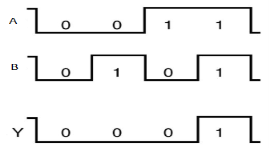
If both inputs are ‘1’, then only the output, Y is ‘1’. For remaining combinations of inputs, the output, Y is ‘0’.
The figure below shows the symbol of an AND gate, which is having two inputs A, B and one output, Y.
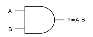
Fig.: AND gate
Timing Diagram:
OR gate
It is a digital circuit which has two or more inputs and a single output which is the logical OR of all those inputs. It is represented with the symbol ‘+’.
The truth table of 2-input OR gate is:
A | B | Y = A + B |
0 | 0 | 0 |
0 | 1 | 1 |
1 | 0 | 1 |
1 | 1 | 1 |
Here A, B are the inputs and Y is the output of two input OR gate.
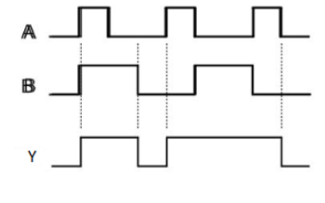
When both inputs are ‘0’, then only the output, Y is ‘0’. For remaining combinations of inputs, the output, Y is ‘1’.
The figure below shows the symbol of an OR gate, which is having two inputs A, B and one output, Y.

Fig: OR gate
Timing Diagram:
NOT gate
It is a digital circuit that has one input and one output. Here the output is the logical inversion of input. Hence, it is also called as an inverter.
The truth table of NOT gate is:
A | Y = A’ |
0 | 1 |
1 | 0 |
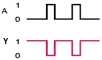
Here A and Y are the corresponding input and output of NOT gate. When A is ‘0’, then, Y is ‘1’. Similarly, when, A is ‘1’, then, Y is ‘0’.
The figure below shows the symbol of NOT gate, which has one input, A and one output, Y.

Fig: NOT gate
Timing Diagram:
Universal gates
- NAND & NOR gates are known as universal gates.
- We can implement any Boolean function by using NAND gates and NOR gates alone.
NAND gate
It is a digital circuit which has two or more inputs and single output and it is the inversion of logical AND gate.
The truth table of 2-input NAND gate is:
A | B | Y = (A.B)’ |
0 | 0 | 1 |
0 | 1 | 1 |
1 | 0 | 1 |
1 | 1 | 0 |
Here A, B are the inputs and Y is the output of two input NAND gate. When both inputs are ‘1’, then the output, Y is ‘0’. If at least one of the input is zero, then the output, Y is ‘1’. This is just the inverse of AND operation.
The image shows the symbol of NAND gate:

Fig: NAND gate
NAND gate works same as AND gate followed by an inverter.
Timing Diagram:

NOR gate
It is a digital circuit that has two or more inputs and a single output which is the inversion of logical OR of all inputs.
The truth table of 2-input NOR gate is:
A | B | Y = (A+B)’ |
0 | 0 | 1 |
0 | 1 | 0 |
1 | 0 | 0 |
1 | 1 | 0 |
Here A and B are the two inputs and Y is the output. If both inputs are ‘0’, then the output is ‘1’. If any one of the input is ‘1’, then the output is ‘0’. This is exactly opposite to two input OR gate operation.
The symbol of NOR gate is:

Fig: NOR gate
NOR gate works exactly same as that of OR gate followed by an inverter.
Timing Diagram:
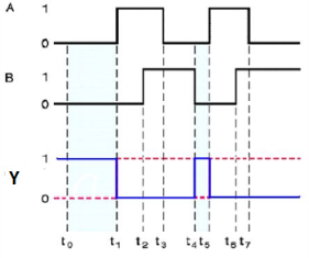
Special Gates
Ex-OR gate
It stands for Exclusive-OR gate. Its function varies when the inputs have even number of ones.
The truth table of 2-input Ex-OR gate is:
A | B | Y = A⊕B |
0 | 0 | 0 |
0 | 1 | 1 |
1 | 0 | 1 |
1 | 1 | 0 |
Here A, B are the inputs and Y is the output of two input Ex-OR gate. The output (Y) is zero instead of one when both the inputs are one.
Therefore, the output of Ex-OR gate is ‘1’, when only one of the two inputs is ‘1’. And it is zero, when both inputs are same.
The symbol of Ex-OR gate is as follows:

Fig: XOR gate
It is similar to that of OR gate with an exception for few combination(s) of inputs. Hence, the output is also known as an odd function.
Timing Diagram:
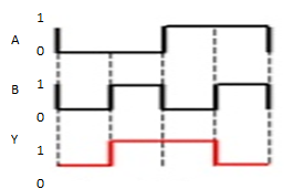
Ex-NOR gate
It stands for Exclusive-NOR gate. Its function is same as that of NOR gate except when the inputs having even number of ones.
The truth table of 2-input Ex-NOR gate is:
A | B | Y = A⊙B |
0 | 0 | 1 |
0 | 1 | 0 |
1 | 0 | 0 |
1 | 1 | 1 |
Here A, B are the inputs and Y is the output. It is same as Ex-NOR gate with the only modification in the fourth row. The output is 1 instead of 0, when both the inputs are one.
Hence the output of Ex-NOR gate is ‘1’, when both inputs are same and 0, when both the inputs are different.
The symbol of Ex-NOR gate is:

Fig: XNOR gate
It is similar to NOR gate except for few combination(s) of inputs. Here the output is ‘1’, when even number of 1 is present at the inputs. Hence is also called as an even function.
Timing Diagram:
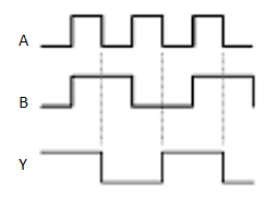
- 7400 Quad 2 input NAND gates
- 7402 Quad 2 input NOR gates
- 7404 Hex NOT gates (Inverters)
- 7408 Quad 2 input AND gates
- 7432 Quad 2 input OR gates
- 7486 Quad 2 input XOR gates
- 747266 Quad 2 input XNOR gates
- 74133 Single 13 input NAND gate
- Half Adder
It is a combinational circuit which has two inputs and two outputs.
It is designed to add two single bit binary number A and B.
It has two outputs carry and sum.
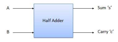
Fig.: Half adder
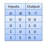
Fig: Truth Table
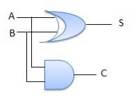
Fig: Circuit Diagram Half adder
Full Adder
- It is developed to overcome the drawback of Half Adder circuit.
- It can add two one-bit numbers A and B and a carry C.
- It is a three input and two output combinational circuit.
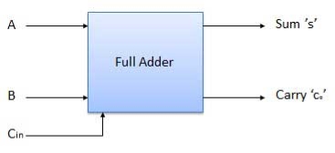
Fig: Block diagram Full adder
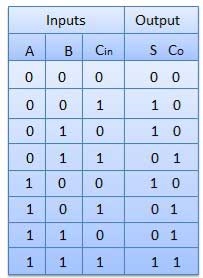
Fig: Truth Table
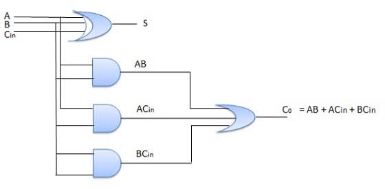
Fig: Circuit Diagram Full adder
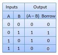
- Half Subtractors
It is a combination circuit with two inputs and two outputs.
The difference between the two binary bits is obtained at the output and an output (Borrow) indicates if a 1 has been borrowed.
Here A is called as Minuend bit and B is called as Subtrahend bit.
Truth Table
Circuit Diagram
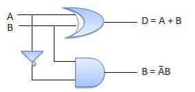
Fig. Half subtractor
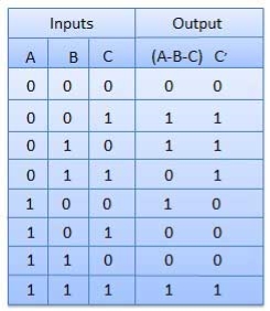
B. Full Subtractors
It is a combinational circuit which has three inputs A, B, C and two output D and C'.
A is the 'minuend', B is 'subtrahend', C is the 'borrow' which is produced by the previous stage, difference output D and C' is the borrow output.
Truth Table
Circuit Diagram
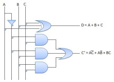
Fig. Full subtractor
Key Takeaways:
- Half adder is a combinational circuit which has two inputs and two outputs.
- Since there is no provision for carry in half adder, full adder is developed to overcome the drawback.
- Half subtractor is a combinational circuit which has two inputs and two outputs.
- Since there is no provision for borrow in half subtractor, full subtractor is developed to overcome the drawback.
- It is a special type of combinational circuit.
- It has n-data inputs, one output and m inputs select lines with 2m = n.
- It selects one of the n data inputs and routes it to the output.
- The selection of one of the inputs is done by the select lines.
- Depending on the code applied at the inputs, one of the n data sources is selected and transmitted to the single output Y.
- E is the enable input which is useful for cascading purpose.
- It is an active low terminal hence performs the required operation when it is low.
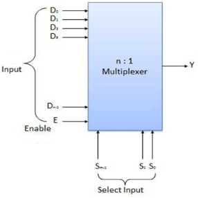
Fig.: Block diagram of multiplexer
Multiplexers come in multiple variations
- 2: 1 multiplexer
- 4: 1 multiplexer
- 16: 1 multiplexer
- 32: 1 multiplexer
Block Diagram of 2:1 MUX
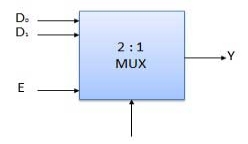
Fig.: 2:1 MUX
Truth Table of 2:1 MUX
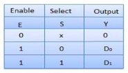
Where x is don’t care.
Key Takeaways
- It has n-data inputs, one output and m inputs select lines with 2m = n.
- The selection of one of the inputs is done by the select lines.
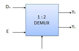
- It performs the inverse operation of a multiplexer as it receives one input and distributes it across its outputs.
- It has only one input and n outputs with m select input.
- At a time only one output line is selected by the select lines and that input is transmitted through the output line.
- It is equivalent to a single pole multiple way switch.
Various Demultiplexers are used as:
- 1: 2 demultiplexer
- 1: 4 demultiplexer
- 1: 16 demultiplexer
- 1: 32 demultiplexer
Block diagram
Truth Table
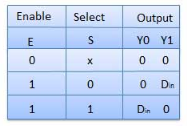
Where x is don’t care.
Key Takeaways:
- It performs the inverse operation of a multiplexer as it receives one input and distributes it across its outputs.
- It has only one input and n outputs with m select input.
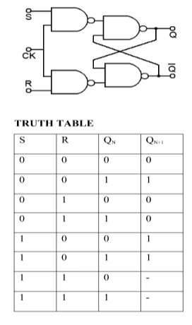
S-R Flip Flop:
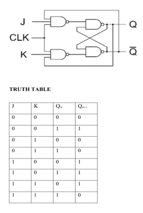
J-K Flip Flop:
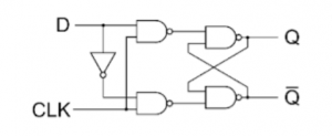
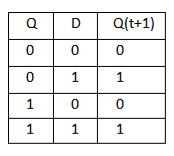
D Flip Flop:
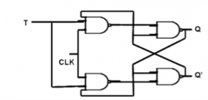
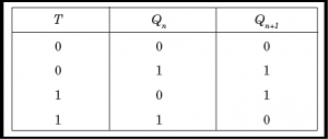
T Flip Flop:
- Some flip-flops have asynchronous inputs that are used to force the flip-flop to a particular state independently of the clock
- The input that sets the flip-flop to 1 is called preset or direct set. The input that clears the flip-flop to 0 is called clear or direct reset.
- When power is turned on in a digital system, the state of the flip-flops is unknown. The direct inputs are useful for bringing all flip-flops in the system to a known starting state prior to the clocked operation.
- The knowledge of the type of flip-flops and a list of the Boolean expressions of the combinational circuit provide the information needed to draw the logic diagram of the sequential circuit. The part of the combinational circuit that gene rates external outputs is described algebraically by a set of Boolean functions called output equations. The part of the circuit that generates the inputs to flip-flops is described algebraically by a set of Boolean functions called flip-flop input equations (or excitation equations).
- The information available in a state table can be represented graphically in the form of a state diagram. In this type of diagram, a state is represented by a circle and the (clock-triggered) transitions between states are indicated by directed lines connecting the circles.
- The time sequence of inputs, outputs, and flip-flop states can be enumerated in a state table (transition table). The table has four parts present state, next state, inputs and outputs.
- In general, a sequential circuit with 'm' flip-flops and 'n' inputs needs 2m+n rows in the state table.
Positive Edge Triggered D Flip-flop
- A circuit diagram of a Positive edge triggered D Flip-flop is shown as below. It has an additional reset input connected to the three NAND gates.
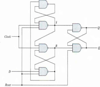
Fig: Circuit Diagram
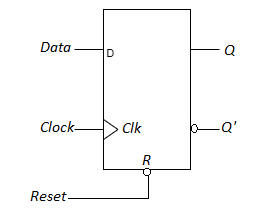
Fig: Symbol
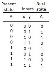
Fig: State Table
- When the reset input is 0 it forces output Q' to Stay at 1 which clears output Q to 0 thus resetting the flip-flop.
- Two other connections from the reset input ensure that the S input of the third SR latch stays at logic 1 while the reset input is at 0 regardless of the values of D and Clk.
- Function table suggests that:
- When R = 0, the output is set to 0 (independent of D and Clock).
- The clock at Clock is shown with an upward arrow to indicate that the flip-flop triggers on the positive edge of the clock.
- The value in D is transferred to Q with every positive-edge clock signal provided that R = 1.
Analysis with D Flip-Flops
- The input equation of a D Flip-flop is given by DA = A ⊕ x ⊕ y. DA means a D Flip-flop with output A.
- The x and y variables are the inputs to the circuit. No output equations are given, which implies that the output comes from the output of the flip-flop.
- The state table has one column for the present state of flip-flop 'A' two columns for the two inputs, and one column for the next state of A.
- The next-state values are obtained from the state equation A (t + 1) = A ⊕ x ⊕ y.
- The expression specifies an odd function and is equal to 1 when only one variable is 1 or when all three variables are 1.
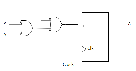
Fig: Circuit Diagram
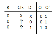
Fig: State Table
Analysis with JK Flip-Flops
- The circuit can be specified by the flip-flop input equations:
- JA = B; KA = Bx'
- JB = x'; KB = A'x + Ax' = A ⊕ x
- The next state of each flip-flop is evaluated from the corresponding J and K inputs and the characteristic table of the JK flip-flop listed as:
- When J = 1 and K = 0 the next state is 1
- When J = 0 and K = 1 the next state is 0
- When J = 0 and K = 0 there is no change of state and the next-state value is the same as that of the present state.
- When J = K = 1, the next-state bit is the complement of the present-state bit.
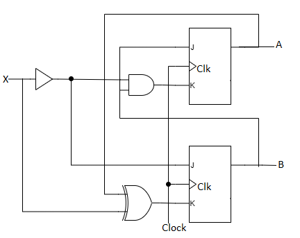
Fig: Circuit Diagram
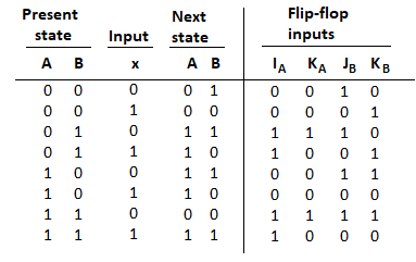
Fig: State Table
- The characteristic equations for the flip-flops are
- A (t + 1) = JA' + K'A
- B (t + 1) = JB' + K'B
- This gives us the state equation of A by substituting the values of JA, KA
A (t + 1) = BA' + (Bx')'A = A'B + AB' + Ax
- The state equation provides the bit values for the column headed "Next State" for A in the state table. Similarly, the state equation for flip-flop B can be derived from the characteristic equation by substituting the values of JB and KB.:
- B (t + 1) = x'B' + (A ⊕ x)'B = B'x' + ABx + A'Bx'
Analysis with T Flip-Flops
- The circuit can be specified by the characteristic equations:
- Q(t+1) = T ⊕ Q = T'Q + TQ'
- The sequential circuit has two flip-flops A and B, one input x, and one output y and can be described algebraically by two input equations and an output equation.
- TA = Bx
- TB = x
- y = AB
- The state table for the circuit is listed below. The values for y are obtained from the output equation. The values for the next state can be derived from the state equations by substituting TA and TB in the characteristic equations yielding:
- A (t + 1) = (Bx)' A + (Bx)A' = AB' + Ax' + A'Bx
- B (t + 1) = x ⊕ B
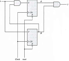
Fig: Circuit Diagram
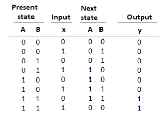
Fig: State Table
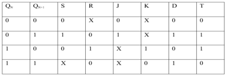
EXCITATION TABLE:
Race Around Condition in JK Flip-flop –
- For J-K flip-flop, if J=K=1, and if clk=1 for a long period of time, then output Q will toggle as long as CLK remains high which makes the output unstable or uncertain.
- This problem is known as race around condition in J-K flip-flop.
- This problem can be avoided by ensuring that the clock input is at logic “1” only for a very short time.
- Hence the concept of Master Slave JK flip flop was introduced.
Master Slave JK flip flop –
It is basically a combination of two JK flip-flops connected together in series.
The first is the “master” and the other is a “slave”.
The output from the master is connected to the two inputs of the slave whose output is fed back to inputs of the master.
In addition to these two flip-flops, the circuit comprises of an inverter.
The inverter is connected to clock pulse in such a way that an inverted clock pulse is given to the slave flip-flop.
In other words, if CP=0 for a master flip-flop, then CP=1 for a slave flip-flop and vice versa.
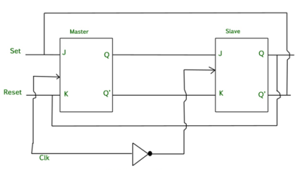
Fig. Master Slave Flip flop
Working of a master slave flip flop –
- When the clock pulse goes high, the slave is isolated; J and K inputs can affect the state of the system. The slave flip-flop is isolated when the CP goes low. When the CP goes back to 0, information is transmitted from the master flip-flop to the slave flip-flop and output is obtained.
- The master flip flop is positive level triggered and the slave flip flop is negative level triggered, hence the master responds prior to the slave.
- If J=0 and K=1, Q’ = 1 then the master goes to the K input of the slave and the clock forces the slave to reset therefore the slave copies the master.
- If J=1 and K=0, Q = 1 then the master goes to the J input of the slave and the Negative transition of the clock sets the slave and thus copy the master.
- If J=1 and K=1, the master toggles on the positive transition and the slave toggles on the negative transition of the clock.
- If J=0 and K=0, the flip flop becomes disabled and Q remains unchanged.
Timing Diagram of a Master flip flop –
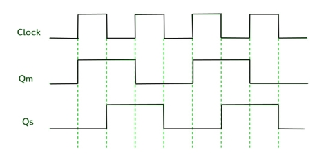
- When the CP = 1 then the output of master is high and remains high till CP = 0 because the state is stored.
- Now the output of master becomes low when the clock CP = 1 and remains low until the clock becomes high again.
- Thus, toggling takes place for a clock cycle.
- When the CP = 1 then the master is operational but not the slave.
- When the clock is low, the slave becomes operational and remains high until the clock again becomes low.
- Toggling takes place during the whole process since the output changes once in a cycle.
- This makes the Master-Slave J-K flip flop a Synchronous device which passes data with the clock signal.
Conversion for flip flops:
i) SR To JK FlipFlop
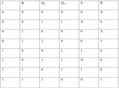
Excitation Functions:
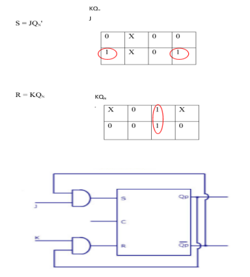
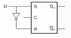
Ii) Convert SR To D Flip Flop:
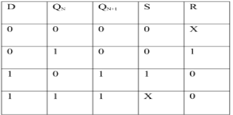
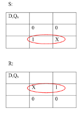
Excitation Functions:
S = D
R = D‘
- Flip flops are used to store one bit of binary data (1or 0).
- If we need to store multiple bits of data, we use multiple flip flops.
- N flip flops are connected to store n bits of data.
- A Register is a device which stores such information. It is a group of flip flops connected in series which is used to store multiple bits of data.
- The information stored in these registers can be transferred with the help of shift registers.
- This register is a group of flip flops used to store multiple bits of data.
- The bits stored in these registers can be moved in/out of the registers by applying clock pulses.
- The registers which shift the bits towards left are called “Shift left registers”.
The registers which shift the bits towards right are called “Shift right registers”.
Shift registers are of 4 types and they are:
- Serial In Serial Out register
- Serial In parallel Out register
- Parallel In Serial Out register
- Parallel In parallel Out register
Applications Of Shift Registers
- They are used for temporary data storage.
- They are used for data transfer and data manipulation.
- The SISO and PIPO registers are used to produce time delay in digital circuits.
- The SIPO register is used for conversion of serial data to parallel data hence they are used in communication lines .
- A PISO register is used to convert parallel data to serial data.
Four types are:
Serial-In Serial-Out Shift Register (SISO) –
- It allows serial input i.e., one bit after another and produces a serial output is known as Serial-In Serial-Out shift register.
- Since it has one output, the data leaves the register one bit at a time in a serial pattern, hence known as Serial-In Serial-Out Shift Register.
- The logic circuit is given underneath.
- The circuit comprises four D flip-flops which are connected serially.
- All these flip-flops are synchronous.

Fig. SISO
SIPO
Serial-In Parallel-Out shift Register (SIPO) –
- It allows serial input through a single data line and produces a parallel output.
- The logic circuit is given underneath.
- The circuit consists of four D flip-flops which are connected synchronously.
- The clear (CLR) signal is also connected to all the 4 flip flops to RESET them.
- The output of the first flip flop is sent to the input of the next and so on.
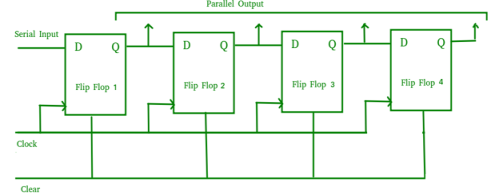
Fig. SIPO
- They are used in communication lines because the main use of the SIPO register is to convert serial data into parallel data.
PISO
Parallel-In Serial-Out Shift Register (PISO) –
- It allows parallel input data and produces a serial output.
- The logic circuit is given underneath.
- The circuit comprises four D flip-flops which are connected synchronously.
- The clock is connected to all the flip flops but the input data is connected to each flip flop individually through a multiplexer.
- The output of the previous flip flop and parallel data input are connected to the input of the MUX and the output of MUX is connected to the next flip flop.
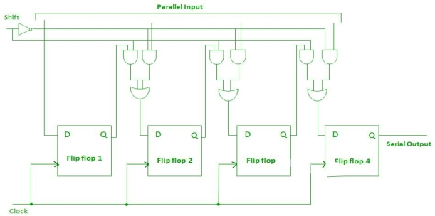
Fig. PISO
- It used to convert parallel data to serial data.
PIPO
Parallel-In Parallel-Out Shift Register (PIPO) –
- It allows parallel input data and produces a parallel output.
- The logic circuit is given underneath.
- The circuit comprises four D flip-flops which are connected synchronously.
- The clear (CLR) and clock signals are connected to all flip flops.
- In this, there are no interconnections between flip-flops as no serial shifting of the data is required.
- Data is provided separately as input for each flip flop and the output is also collected individually from each flip flop.
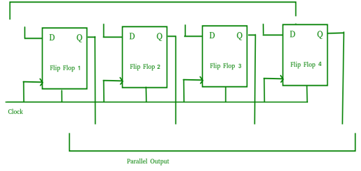
Fig. PIPO
- It is used as a temporary storage device and it acts as a delay element too.
A Counter stores the number of times a particular event or process has occurred in relationship to a clock signal.
They are used in digital electronics for counting purpose.
They can count specific event happening how many times in the circuit.
For example, in UP counter count increases for every rising edge of clock.
A counter can follow certain sequence based on our design like any sequence 0,1,3,2… .
They can be designed with the help of flip flops.
Counter Classification
Counters are broadly classified into two categories:
- Asynchronous counter
- Synchronous counter
1. Asynchronous Counter
In this universal clock is not used and only the first flip flop is driven by main clock and the clock input of rest of the following is driven by output of previous flip flops.

Fig. Asynchronous counter
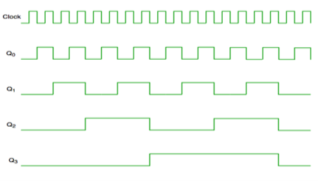
Fig. Timing diagram of Asynchronous counter
It is seen from timing diagram that Q0 is changing as soon as the rising edge of clock pulse is encountered.
Q1 is changing when rising edge of Q0 is encountered and so on.
In this way ripples are generated through Q0,Q1,Q2,Q3 and therefore it is also called as a RIPPLE counter.
2. Synchronous Counter
It has one global clock which drives each and every flip flop and hence output changes in parallel.
The advantage of synchronous counter over asynchronous counter is that it can operate on higher frequency and it does not have cumulative delay .
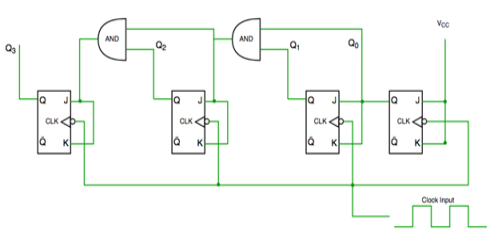
Fig. Synchronous counter
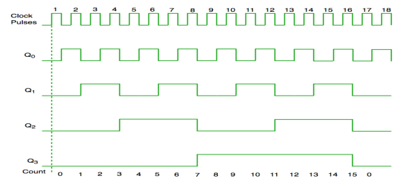
Fig. Timing diagram of synchronous counter
Microprocessor: Introduction
- It is a controlling unit that is fabricated on a small chip.
- It is capable to perform arithmetic logic operations and communicate with various devices connected to it.
- It comprises of an ALU (Arithmetic Logic Unit), MU (Memory unit) and CU (Control unit).
- It also consists of register array with registers named as B, C, D, E, H, L and ACC.
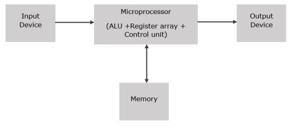
Fig.: Basic block diagram of microprocessor
Microcontroller: Introduction
- Microcontroller is a compact tiny computer that is fabricated inside a chip and is used in automatic control systems including security systems, office machines, power tools, alarming system, traffic light control, washing machine, and much more.
- It is economical programmable logic control that can be interfaced with external devices in order to control the devices from a distance.
- It was specially built for embedded system and consisted of read write memory, read only memory, I/O ports, processor and built in clock.
- C and assembly languages are used to program the microcontrollers.
- There are also other languages available to program the microcontroller but at the start learning a microcontroller programming with C and assembly language is a great choice, both are easy to learn and provide a clear concept about microcontroller.
- Technology have been evolved in an amazing way and made our lives easier more than ever before.
References:
1. Integrated Devices & Circuits by Millman & Halkias, TMH Publications.
2. Electronics Devices and Circuit Theory by R. Boylestad & L. Nashelsky, Pearson Publication
3. Electronic Communication System by G. Kennedy, TMH Publications.
4. Basic Electronics by Sanjeev Kumar & Vandana Sachdeva, Paragaon International Publication