Unit - 4
Power electronic devices & Communication engineering
The silicon controlled rectifier (SCR) is a three-terminal semiconductor switching. It is considered important circuit element after the diode and the transistor. This name is given to this device because it is made of silicon and is used as a rectifier and that rectification can be controlled.
Silicon controlled rectifier is a semiconductor device that acts as a true electronic switch. It can change alternating current into direct current and simultaneously can control the amount of powered to the load. Thus SCR combines the features of a rectifier and a transistor.
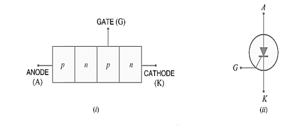
Figure 1: (i) construction (ii) the symbol of SCR.
Construction
The three pn junction device is called a silicon-controlled rectifier. It is formed as when a pn junction is added to a junction transistor, It is an ordinary rectifier (pn) and a junction transistor (npn) combined in one unit to form pn pn device.
There are three terminals
- One from the outer p-type material called anode.
- A second from the outer n-type material called cathode K.
- The third from the base of transistor section and is called gate G.
In the normal operating conditions of SCR, anode is held at high positive potential w.r.t. Cathode and gate at small positive potential w.r.t. Cathode.
The silicon-controlled rectifier is a solid state equivalent of thyratron. The gate, anode and cathode of SCR correspond to the grid, plate and cathode of thyratron. For this reason, SCR is sometimes called thyristor.
Working
In a silicon-controlled rectifier, load is connected in series with anode. The anode is always kept at positive potential w.r.t. Cathode.
The device is made of silicon because leakage current in silicon is very small as compared to germanium.
The device is used as a switch, it will carry leakage current in the off condition which should be as small as possible.
- When gate is open: In case of open gate no voltage applied to the gate. When gate is open, junction J2 is reverse biased while junctions J1 and J3 are forward biased. Hence, the situation in the junctions J1 and J3 is just as in a npn transistor with base open. Consequently, no current flows through the load RL and the SCR is cut off. However, if the applied voltage is gradually increased, a stage is reached when reverse biased junction J2 breaks down. The SCR is in the ON state i.e. conducts heavily. The applied voltage at which SCR conducts heavily without gate voltage is called Break over voltage. Figure shows the SCR circuit with gate open.
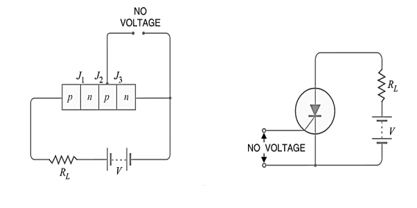
Figure 2: When gate is open
- When gate is positive w.r.t. Cathode: In this case junctionJ3 is forward biased and junction J2 is reverse biased. Now the electrons from n-type material start moving across junction J3 towards left whereas holes from p-type towards the right. Consequently, the electrons from junction J3 are attracted across junction J2 and gate current starts flowing.
As soon as the gate current flows, anode current increases. The increased anode current in turn makes more electrons available at junction J2. This process continues and in an extremely small time, junction J2breaks down and the SCR starts conducting heavily.
Once SCR starts conducting, the gate loses all control. Even if gate voltage is removed, the anode current does not decrease at all. The only way to stop conduction i.e. bring SCR in off condition by reducing the applied voltage to zero.
So the SCR can be made to conduct heavily at smaller applied voltage by applying a small positive potential to the gate as shown in Figure 6.
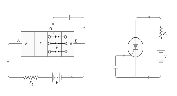
Figure 3: When gate is positive w.r.t. Cathode
The following conclusions are drawn from the working of SCR
(i)SCR behaves like a switch. An SCR work between two states i.e. either it does not conduct or it conducts heavily. There is no state in between.
(ii)There are two ways to turn on the SCR. The first method is to keep the gate open and make the supply voltage equal to the breakover voltage. The second method is to operate SCR with supply voltage less than breakover voltage and then turn it on by means of a small voltage applied to the gate.
(iii)Applying small positive voltage to the gate is the normal way to close an SCR because the breakover voltage is usually much greater than supply voltage.
(iv)To open the SCR (i.e. to make it non-conducting), reduce the supply voltage to zero.
Equivalent Circuit of SCR
The SCR shown in Figure 7(ii) can be visualised as separated into two transistors as shown in
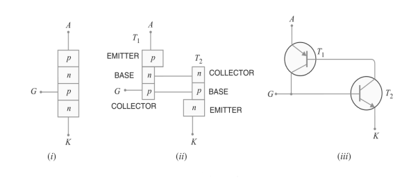
Figure 4: (i) construction of SCR (ii) Thus, the equivalent circuit of SCR is composed of pnp transistor and npn transistor connected as shown in (iii) It is clear that collector of each transistor is coupled to the base of the other, thereby making a positive feedback loop.
Characteristics
It is the curve between anode-cathode voltage (V) and anode current (I)of an SCR at constant gate current. Figure 8 shows the characteristics of SCR.
(i) Forward characteristics: When anode is positive w.r.t. Cathode, the curve between V and I is called the forward characteristic. In Figure 8 OABC is the forward characteristic of SCR at IG=0. If the supply voltage is increased from zero, a point is reached (point A) when the SCR starts conducting. Under this condition, the voltage across SCR suddenly drops as shown by dotted curve AB and most of supply voltage appears across the load resistance RL. If proper gate current is made to flow, SCR can close at much smaller supply voltage.
(ii) Reverse characteristics: When anode is negative w.r.t. Cathode, the curve between V and I is known as reverse characteristic. The reverse voltage does come across SCR when it is operated with a.c. Supply. If the reverse voltage is gradually increased, at first the anode current remains small (i.e. leakage current) and at some reverse voltage, avalanche breakdown occurs and the SCR starts conducting heavily in the reverse direction as shown by the curve DE. This maximum reverse voltage at which SCR starts conducting heavily is known as reverse breakdown voltage.
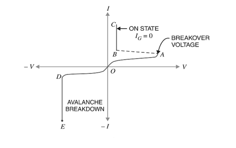
Figure 5: Characteristics of SCR
Applications of SCR
The ability of an SCR to control large currents in a load by means of small gate current makes this device useful in switching and control applications. Some of the important applications of SCR are:
- An important application of SCR is for switching operations. As SCR has no moving parts, therefore, when it is used as a switch, it is often called a static contactor.
- SCR used for power control. It is often necessary to control power delivered to some load such as the heating element of a furnace. Series resistances or potentiometers cannot be used because they waste power in high power circuits. Under such conditions, silicon controlled rectifiers are used which are capable of adjusting the transmitted power with little waste.
- SCRs used for speed control of d.c. Shunt motor. The conventional method of speed control of d.c. Shunt motor is to change the field excitation. But change in field excitation changes the motor torque also. This drawback is overcome in SCR control.
- SCR used for overlight detection.
- SCR Crowbar. A crowbar is a circuit that is used to protect a voltage-sensitive load from excessive d.c. Power supply output voltages.
Key Takeaways
- The three pn junction device is called a silicon controlled rectifier.
- Silicon controlled rectifier is a semiconductor device that acts as a true electronic switch.
- There are three terminals one from the outer p-type material called anode, a second from the outer n-type material called cathode K, the third from the base of transistor section and is called gate G.
- In the normal operating conditions of SCR, anode is held at high positive potential w.r.t. Cathode and gate at small positive potential w.r.t. Cathode.
- In case of open gate, no voltage applied to the gate. When gate is open, junction J2 is reverse biased while junctions J1 and J3 are forward biased.
- When gate is positive w.r.t. Cathode junction J3 is forward biased and junction J2 is reverse biased.
- SCR behaves like a switch. An SCR work between two states i.e. either it does not conduct or it conducts heavily. There is no state in between.
- Applying small positive voltage to the gate is the normal way to close an SCR because the break over voltage is usually much greater than supply voltage.
- To open the SCR (i.e. to make it non-conducting), reduce the supply voltage to zero.
- When anode is positive w.r.t. Cathode, the curve between V and I is called the forward characteristic.
- When anode is negative w.r.t. Cathode, the curve between V and I is known as reverse characteristic.
DIAC
DIAC simply means diode alternating current or diode ac switch. The DIAC is nothing but the combination of two SCRs connected back to back. So A DIAC is a two-terminal device that can act as a switch based on the voltage applied across it.
We already studied that the TRIAC being used to switch current in both directions. But TRIACs cannot fire/trigger symmetrically it is accompanied by a support component called DIAC. Generally, DIAC uses to trigger the TRIAC. Sometimes it is also known as a TRIAC without GATE terminal.
SYMBOL OF DIAC
The symbol of DIAC is as shown in figure.
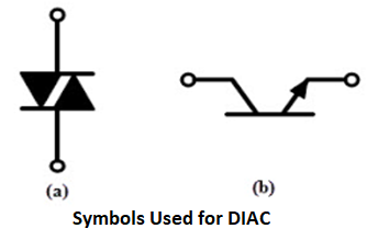
Figure 6: Symbol of DIAC
DIAC is given by the symbol of two Diodes connected in parallel and opposite to one another and has two terminals. Since the DIAC is bidirectional.
These two terminals can’t be named as anode and cathode, these terminals are labelled MT1 and MT2 where MT stands for Main terminals or simply M1 and M2. In some books terminals are labelled as A1 and A2. Just like a resistor or ceramic capacitor the pinouts of DIAC are reversible.
Construction
We already know that the DIAC is a two-terminal device. Diac is simply a combination of parallel semiconductor layers that allows activating in one direction. It can deliver current flow in both directions. DIAC consists of two terminals namely MT1 and MT2. The Structure is similar to that of transistor, but difference is the DIAC does not have any base terminal. A DIAC has two p-type material and three n-type materials and it does not have any gate terminal in it.
The three region have the same amount of doping and it delivers symmetrical switching properties in both the polarities of the applied voltage. The layers closer to the terminals are the combination of both positive and negative layers. When the voltage is passed to the terminals the layer with respective polarity to the voltage gets activated, this combination of both the polarities helps in operating the DIAC in both the directions
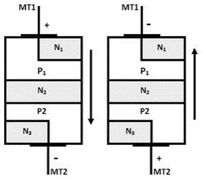
Figure 6: Construction of DIAC
Working
When a voltage of either polarity is applied to a diac, one junction is forward-biased and the other is reverse-biased. The current is limited by the leakage current of the reverse-biased junction. When the applied voltage is sufficiently large, breakdown occurs at BVCBO(1 -  , where BVCBOis the avalanche breakdown voltage of the p-n junction, the common-base current gain, and it is a constant. This expression is the same for the breakdown voltage of an open base n-p-n transistor.
As the current increases after breakdown,  will increase, causing a reduction of the terminal voltage. This reduction gives rise to the negative region. The bidirectional p-n-p-n diode switch behaves like two conventional Shockley diodes connected in antiparallel to permit the accommodation to voltage signals of two polarities, as in figure 16(a), where M1 stands for main terminal 1, and M2 for main terminal 2. Using the shorted-cathode principle, we can integrate this arrangement into a single two-terminal diac as shown in Figure 16(b). The symmetry of this structure results in identical performance for either polarity of applied voltage. The diac can be triggered into conduction by exceeding the breakover voltage or by dV/dt triggering. Because of its regenerative action, the indirection p-n-p-n diode switch has a larger negative resistance and smaller forward drop than that of an ac trigger diode.
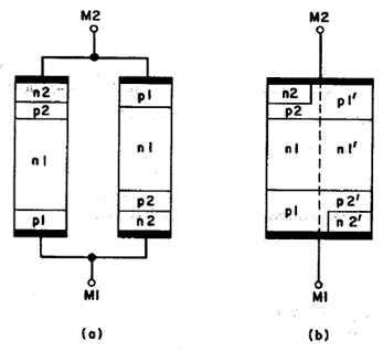
Figure 7: (a) Two shockley devices are connected antiparallel (b) Integration of the diodes into two terminal single device Construction of DIAC
Characteristics
Curve of the DIAC will be in the shape of a Z and the curve will be lying on the first and third quadrants because they conduct in both the positive and negative polarity. The First quadrant represents the positive half cycle where the current will be flowing from MT1 to MT2 (or M1 to M2) and the second quadrant represents the negative half cycle where the current will be flowing from MT2 to MT1(or M2 to M1). The symmetrical I-V characteristics are shown in Figure.
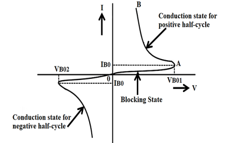
Figure 8: I-V characteristics of DIAC
Initially, because of the Reverse Biasing between the layers there will be small leakage current flowing through the DIAC i.e. the resistance of the DIAC will be higher. It is called as the blocking state in the curve.
Once the applied voltage reaches the breakdown voltage the resistance of the DIAC drops abruptly and then it starts conducting which leads to a sharp decrease in voltage and the current starts increasing, which is mentioned as a conduction state in the curve.
The DIAC will be in the conducting state until the current reaches the particular value called the holding current, where holding current is the minimum current that required for a device to keep it in the ON state.
The DIAC acts as an open circuit when the voltage is less than its avalanche breakdown voltage. When the device has to be turned off, the voltage must be reduced below its avalanche breakdown voltage.
Application of DIAC
The main application of a DIAC is its use in a TRIAC triggering circuit. The DIAC is connected to the gate terminal of the TRIAC. When the voltage across the gate decreases below a predetermined value, the gate voltage will be zero and hence the TRIAC will be turned off. When the applied voltage across the DIAC increases above the avalanche breakdown voltage, only then it can conduct.
DIAC can be used in the lamp dimmer circuit, in a heat control circuit and in the speed control of a universal motor
Key Takeaways
- Triac can conduct in both the directions that is whether the applied gate signal is positive or negative.
- Triac is a three terminal AC switch and it is different from the other silicon controlled rectifiers.
- Triac is bilateral since it works for both the polarities. Triac do not have anode and cathode.
- The gate terminal is the control terminal. The flow of current in the triac is bi directional that means current can flow in both the directions.
- The TRIAC device operations under various biasing conditions are illustrated as:
- When the main terminal M1 is positive with respect to M2 and a positive voltage is applied to the gate (also with respect to M2
- M1 is positive with respect to M2, but a negative voltage is applied to the gate:
- When Ml is negatively biased with respect to M2 and VG is positively biased:
- Ml negative with respect to M2 and VG is also negative
- DIAC simply means diode alternating current or diode ac switch.
- The DIAC is nothing but the combination of two SCRs connected back to back. So A DIAC is a two-terminal device that can act as a switch based on the voltage applied across it.
- Generally, DIAC uses to trigger the TRIAC. Sometimes it is also known as a TRIAC without GATE terminal.
- Initially, because of the Reverse Biasing between the layers there will be small leakage current flowing through the DIAC i.e. the resistance of the DIAC will be higher. It is called as the blocking state in the curve.
- Once the applied voltage reaches the breakdown voltage the resistance of the DIAC drops abruptly and then it starts conducting which leads to a sharp decrease in voltage and the current starts increasing, which is mentioned as a conduction state in the curve.
- The main application of a DIAC is its use in a TRIAC triggering circuit.
TRIAC
Triac can conduct in both the directions that is whether the applied gate signal is positive or negative. Triac is a three terminal AC switch and itis different from the other silicon-controlled rectifiers. This is a three terminal, four layer, bi-directional semiconductor device that controls AC power. Schematic Symbol of Triac is shown in figure
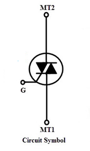
Figure 9: Schematic Symbol of Triac
Construction
It consists of three terminals namely, main terminal 1(MT1orM1), main terminal 2(MT2orM2), and gate terminal G. Triac is bilateral since it works for both the polarities. Triac do not have anode and cathode.
In the structure of triac, two SCRs are connected in the anti-parallel and it will act like a switch for both the directions. Gate terminals is connected to both the N and P regions due to which gate signal may be applied which is irrespective of the polarity of the signal
Here the gate terminal is the control terminal. The flow of current in the triac is bi directional that means current can flow in both the directions.
The triac structure is considerably more complicated than a conventional thyristor. In addition to the p1-n 1-p2-n2 basic four layers, there are a junction gate n3 region and a n4 region in contact with M1. Note also that p1 is shorted to n4, p2 is shorted to n2, and n3 is shorted to p2 by M1, M2, and the gate electrode, respectively.
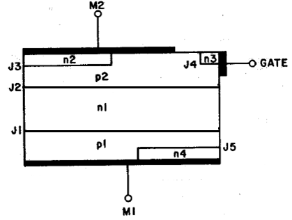
Figure 10: Basic Structure of Triac
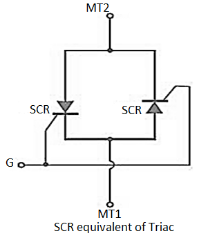
Figure 11: SCR equivalent of Triac
Working
Triac can switch the current in either direction by applying low voltage or by low current pulse of either polarity between the gate and one of the two main terminals M1 and M2. The device operations under various biasing conditions are illustrated as:
- When the main terminal M1 is positive with respect to M2 and a positive voltage is applied to the gate (also with respect to M2): in this case the device behaviour is identical to that of a conventional thyristor. The junction J4 is reverse-biased and is inactive; the gate current is supplied through the gate short near the n3 region. Since junction J5 is also reverse-biased and inactive, the main current is carried through the left side of p1-n 1-p2-n2 section. Shown in Figure 11(a)
- M1 is positive with respect to M2, but a negative voltage is applied to the gate: The junction J4 between n3 and p2 is now forward-biased, and electrons are injected from the n3 to p2. The auxiliary thyristor pl-nl-p2-n3will be turned on by the flow of the lateral base current in p2 toward the n3 gate because of the gain increase in the transistor n3-p2-nl. Full conduction of this auxiliary thyristor results in the current flowing out of this device and toward the n2 region. This current will provide the required gate current and trigger the left-side p1-n1-p2-n2 thyristor into conduction. . Shown in Figure 11(b)
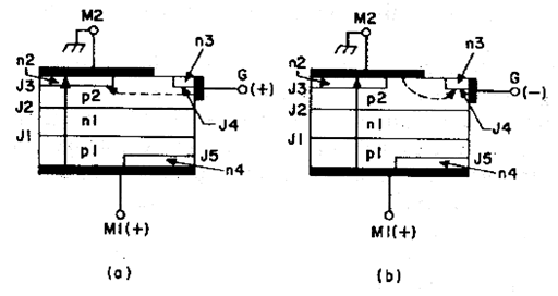
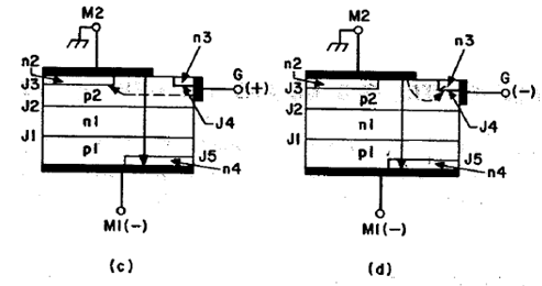
Figure 12: Current flow in four different triggering modes in Triac
Iii. When Ml is negatively biased with respect to M2 and VG is positively biased: In this case the junction J3 becomes forward-biased between M2 and the shorted gate. Electrons are injected from n2 to p2 and diffuse to nl, resulting in an increase of the forward bias of J2. By the regenerative action, eventually full current is carried through the short at M2. The gate junction J4 is reverse-biased and is inactive. The full device current is carried through the right-side p2-nl-pl-n4 thyristor. Shown in Figure 11(c)
Iv. Ml negative with respect to M2 and VG is also negative: In this condition, the junction J4 is forward-biased, and triggering is initiated by injection of electrons from n3 to n1 region. This action lowers the potential at n1, causing holes to be injected from p2 into it n1 region. These holes provide the base current drive for the p2-n1-p1 transistor, and the right side p2-n1-p1-n4 thyristor is eventually turned on since J3 is reverse-biased, the main current is carried from the short at M2 through the n4 region. Shown in Figure 11(d)
Characteristics
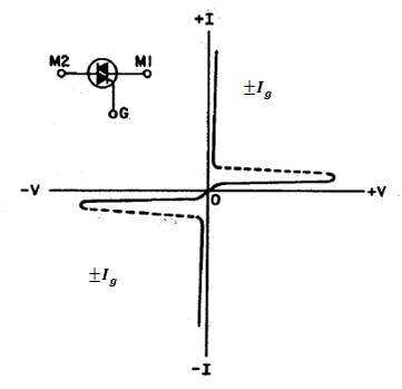
Figure 13: Current–Voltage Characteristics of a triac
The gate trigger may occur in any four quadrant modes of operation. If the device is in ON state the conduction permits a huge amount of current to flow through it.
The current–voltage characteristics of a triac are shown in Figure 13. The supply voltage of the triac to switch ON depends upon the gate current. The triac is a symmetrical triode switch that can control loads supplied with ac power. The V-I characteristics of triac in the first and third quadrants are basically equal to those of an SCR in the first quadrant. It can be functioned with either +Ve or –Ve gate control voltage but in typical operation generally the gate voltage is +Ve in first quadrant and -Ve in third quadrant.
A large amount of current is controlled by the resistance, otherwise, the device may be damaged. With the device, the gate is a control terminal and the proper signal is applied to the gate, therefore the firing angle of the device is controlled.
Applications
TRIAC (Triode for AC) is the semiconductor device widely used in power control and switching applications. The triac is very useful in light dimming, motor speed control, temperature control, and other applications. It finds applications in switching, phase control, chopper designs, brilliance control in lamps, speed control in fans, motors etc.
It is a three-terminal silicon diode. As its name indicates, it has only one P-N junction. It differs from an ordinary diode in that it has three leads and it differs from a FET in that it has no ability to amplify. However, it has the ability to control a large ac power with a small signal. It is a three-terminal silicon diode. As its name indicates, it has only one P-N junction. It differs from an ordinary diode in that it has three lead sand it differs from a FET in that it has no ability to amplify. However, it has the ability to control a large ac power with a small signal.
Construction
A slab of lightly doped (increased resistance characteristic) n-type silicon material has two base contacts attached to both ends of one surface and an aluminum rod alloyed to the opposite surface. The p-n junction of the device is formed at the boundary of the aluminum rod and the n-type silicon slab. The single p-n junction accounts for the terminology unijunction. It was originally called a duo (double) base diode due to the presence of two base.
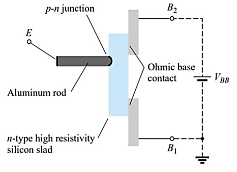
Fig 14 UJT
INTER-BASE RESISTANCE (RBB)
It is the resistance between B2 and B1 i.e. it is the total resistance of the silicon bar from one end to the other with emitter terminal open. It should also be noted that point A is such that RB1 > RB2 . Usually, RB1 = 60% of RB1. The resistance RB1 has been shown as a variable resistor because its value varies inversely as
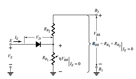
Fig 15 Inter base resistance RBB
As seen from Fig, when a battery of 30 V is applied across B2 B1, there is a progressive fall of voltage over RBB provided E is open. It is obvious from Fig. That emitter acts as a voltage-divider tap on fixed resistance RBB. With emitter open, I1 = I2, the inter-base current is given by Ohm’s Law. I1= I2=VBB /RBB. It may be noted that part of VBB is dropped over RB2 and part on RB1. Let us call the voltage drop across RB1 as VA. Using simple voltage divider relationship, The voltage division factor is given a special symbol (η) and the name of ‘intrinsic standoff ratio.
UJT Static Emitter Characteristics
The decrease in resistance in the active region is due to the holes injected into the n-type slab from the aluminum p-type rod when conduction is established. The increased hole content in the n-type material will result in an increase in the number of free electrons in the slab, producing an increase in conductivity (G) and a corresponding drop in resistance (R ↓ 1/G ↑). Three other important parameters for the unijunction transistor are IP, VV, and IV. Each is indicated on Fig.
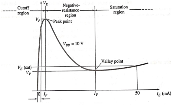
Fig 16 Characteristics of UJT
When VBB is switched on, VA is developed and reverse-biases the junction. If VB is the barrier voltage of the P-N junction, then total reverse bias voltage is = VRB1 + VB = ηVBB + VB Value of VB for Si is 0.7 V. It is obvious that emitter junction will not become forward-biased unless its applied voltage VE exceeds (ηVBB+ VB). This value of VE is called peakpoint voltage VP. When VE = VP, emitter (peak current), IP starts to flow through RB1 to ground (i.e. B1). The UJT is then said to have been fired or turned ON.
Beyond the valley point, UJT is in saturation and VE increases very little with an increasing IE. It is seen that only terminals E and B1 are the active terminals whereas B2 is the bias terminal i.e. it is meant only for applying external voltage across the UJT. Generally, UJT is triggered into conduction by applying a suitable positive pulse at its emitter.
Key takeaway
One unique property of UJT is that it can be triggered by (or an output can be taken from) any one of its three terminals. Once triggered, the emitter current IE of the UJT increases regeneratively till it reaches a limiting value determined by the external power supply. Because of this particular behaviour, UJT is used in a variety of circuit applications.
Introduction of Operational Amplifier (Ic741)
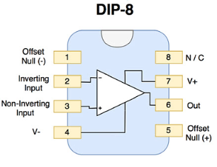
The IC 741 is a small chip. It comprises eight pins. 2, 3 and 6 numbered pins are most significant.
Pin 2 is inverting terminal.
Pin 3 is non-inverting terminal.
Pin 6 is output terminal.
IC 741 mainly performs mathematical operations like addition, subtraction, division, multiplication, integration, differentiation etc. IC 741 has three stages such as differential input, gain, and push-pull output.
Pin 1 and 5 are “offset null” or “balance” terminals.
The op amp is nothing but a differential amplifier. When we apply the same voltage at the inverting terminal (Pin 2) and the non-inverting terminal (Pin 3) there should not be any voltage at the output terminal (Pin 6). This condition is an ideal.
Practically there is always a small voltage (offset voltage) appears at pin 6 even the voltage applied at pin 2 and 3 are exactly equal. Offset voltage appears at output because we cannot make the parameters of transistors and value of biasing resistances of differential amplifier perfectly same.
Characteristics and applications of Operational Amplifier (Ic741)
Transfer characteristics of Op-Amp

Fig 17 Transfer characteristics of ideal op-amp
Open Loop Gain (Avo)
The main function of an operational amplifier is to amplify the input signal and the more open loop gain it has the better. Open-loop gain is the gain of the op-amp without positive or negative feedback and for such an amplifier the gain will be infinite
Input impedance (ZIN)
Input impedance is the ratio of input voltage to input current and is assumed to be infinite to prevent any current flowing from the source supply into the amplifiers input circuitry ( IIN = 0 ). Real op-amps have input leakage currents from a few pico-amps to a few milli-amps.
Output impedance (ZOUT)
The output impedance of the ideal operational amplifier is assumed to be zero acting as a perfect internal voltage source with no internal resistance so that it can supply as much current as necessary to the load.This internal resistance is effectively in series with the load thereby reducing the output voltage available to the load. Real op-amps have output impedances in the 100-20kΩ range.
Bandwidth (BW)
An ideal operational amplifier has an infinite frequency response and can amplify any frequency signal from DC to the highest AC frequencies, so it is therefore assumed to have an infinite bandwidth.
With real op-amps, the bandwidth is limited by the Gain-Bandwidth product (GB), which is equal to the frequency where the amplifiers gain becomes unity.
Offset Voltage (VIO)
The amplifiers output will be zero when the voltage difference between the inverting and the non-inverting inputs is zero, the same or when both inputs are grounded. Real op-amps have some amount of output offset voltage.
Key takeaway
- High input resistance
- Lower output resistance
- Infinite voltage amplification
- Under a certain supply voltage condition, the amplifier can only work in closed-loop (negative feedback) mode.
Applications of Op-Amp
Op-Amp based V-I and I-V converters
A voltage to current converter or V to I converter, is an electronic circuit that takes current as the input and produces voltage as the output.
An op-amp based voltage to current converter produces an output current when a voltage is applied to its non-inverting terminal. The circuit diagram of an op-amp based voltage to current converter is shown in the following figure.
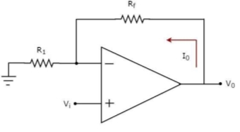
Fig 18 V-I Converter
In the circuit shown above, an input voltage Vi is applied at the non-inverting input terminal of the op-amp.
According to the virtual short concept, the voltage at the inverting input terminal of an op-amp will be equal to the voltage at its non-inverting input terminal.
So, the voltage at the inverting input terminal of the op-amp will be Vi.
The nodal equation at the inverting input terminal's node is −
ViR1−I0=0
=>I0=VtR1
Thus, the output current I0 of a voltage to current converter is the ratio of its input voltage Vi and resistance R1.
We can re-write the above equation as −
I0/Vi=1/R1
The above equation represents the ratio of the output current I0 and the input voltage Vi & it is equal to the reciprocal of resistance R1. The ratio of the output current I0 and the input voltage Vi is called as Transconductance.
Current to voltage converter
A current to voltage converter or I to V converter is an electronic circuit that takes current as the input and produces voltage as the output.
An op-amp based current to voltage converter produces an output voltage when current is applied to its inverting terminal. The circuit diagram of an op-amp based current to voltage converter is shown in the following figure.
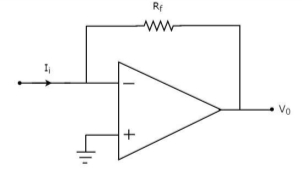
Fig 19 I-V Converter
In the circuit shown above, the non-inverting input terminal of the op-amp is connected to ground. That means zero volts is applied at its non-inverting input terminal.
According to the virtual short concept, the voltage at the inverting input terminal of an op-amp will be equal to the voltage at its non-inverting input terminal. So, the voltage at the inverting input terminal of the op-amp will be zero volts.
The nodal equation at the inverting terminal's node is −
−Ii+0−V0/Rf=0
−Ii=V0/Rf
V0=−Rf.Ii
Thus, the output voltage, V0 of current to voltage converter is the (negative) product of the feedback resistance, Rf and the input current, It. Observe that the output voltage, V0 is having a negative sign, which indicates that there exists a 1800 phase difference between the input current and output voltage.
We can re-write the above equation as –
V0/Ii=−Rf
The above equation represents the ratio of the output voltage V0 and the input current Ii, and it is equal to the negative of feedback resistance, Rf. The ratio of output voltage V0 and input current Ii is called as Trans-resistance.
Key takeaways
A voltage to current converter or V to I converter, is an electronic circuit that takes current as the input and produces voltage as the output.
An op-amp based voltage to current converter produces an output current when a voltage is applied to its non-inverting terminal.
A current to voltage converter or I to V converter is an electronic circuit that takes current as the input and produces voltage as the output.
An op-amp based current to voltage converter produces an output voltage when current is applied to its inverting terminal.
Instrumentation amplifier
The Instrumentation amplifiers consist of three op-amps. In this circuit, a non-inverting amplifier is connected to each input of the differential amplifier.
This instrumentation amplifier provides high input impedance for exact measurement of input data from transducers. The circuit diagram of an instrumentation amplifier is as shown in the figure below.
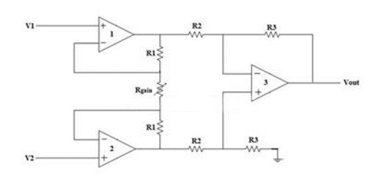
Fig 20 Instrumentation Amplifier
The op-amps 1 & 2 are non-inverting amplifiers and together form an input stage of the instrumentation amplifier. The op-amp 3 is a difference amplifier that forms the output stage of the instrumentation amplifier.
Working
The output stage of the instrumentation amplifier is a difference amplifier, whose output Vout is the amplified difference of the input signals applied to its input terminals.
If the outputs of op-amp 1 and op-amp 2 are Vo1 and Vo2 respectively, then the output of the difference amplifier is given by,
Vout = (R3/R2) (Vo1-Vo2)
The expressions for Vo1 and Vo2 can be found in terms of the input voltages and resistances.
Consider the input stage of the instrumentation amplifier as shown in the figure below.
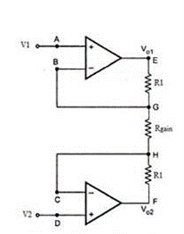
Fig 21 Input Stage of Instrumentation Amplifier
The potential at node A is the input voltage V1. Hence the potential at node B is also V1, from the virtual short concept. Thus, the potential at node G is also V1.
The potential at node D is the input voltage V2. Hence the potential at node C is also V2, from the virtual short. Thus, the potential at node H is also V2.
Ideally the current to the input stage op-amps is zero. Therefore, the current I through the resistors R1, Rgain and R1 remains the same.
Applying Ohm’s law between the nodes E and F,
I = (Vo1-Vo2)/(R1+Rgain+R1) ——————— 1
I = (Vo1-Vo2)/(2R1+Rgain)
Since no current is flowing to the input of the op-amps 1 & 2, the current I between the nodes G and H can be given as,
I = (VG-VH)/Rgain = (V1-V2)/Rgain ————————- 2
Equating equations 1 and 2,
(Vo1-Vo2)/(2R1+Rgain) = (V1-V2)/Rgain
(Vo1-Vo2) = (2R1+Rgain) (V1-V2)/Rgain —————— 3
The output of the difference amplifier is given as,
Vout = (R3/R2) (Vo1-Vo2)
Therefore, (Vo1 – Vo2) = (R2/R3) Vout
Substituting (Vo1 – Vo2) value in the equation 3, we get
(R2/R3) Vout = (2R1+Rgain) (V1-V2)/Rgain
i.e. Vout = (R3/R2) {(2R1+Rgain)/Rgain} (V1-V2)
The above equation gives the output voltage of an instrumentation amplifier. The overall gain of the amplifier is given by the term (R3/R2) {(2R1+Rgain)/Rgain}.
Advantages
- The gain of a three op-amp instrumentation amplifier circuit can be easily varied and controlled by adjusting the value of Rgain without changing the circuit structure.
- The gain of the amplifier depends only on the external resistors used. Hence, it is easy to set the gain accurately by choosing the resistor values carefully.
- The input impedance of the instrumentation amplifier is dependent on the non-inverting amplifier circuits in the input stage. The input impedance of a non-inverting amplifier is very high.
- The output impedance of the instrumentation amplifier is the output impedance of the difference amplifier, which is very low.
- The CMRR of the op-amp 3 is very high and almost all of the common mode signal will be rejected.
Key takeaways
This instrumentation amplifier provides high input impedance for exact measurement of input data from transducers. The output impedance of the instrumentation amplifier is the output impedance of the difference amplifier, which is very low.
Inverting Summing Amplifier
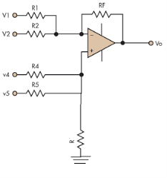
Fig 22: Summing amplifier
- In the above figure, each terminal is connected with two input sources through resistors. V1 and V2 is connected to the inverting terminal and V4 and V5 is connected to the non-inverting terminal.
- Assuming R1=R2=R4=R5=RF=R.
- Now, on applying superposition theorem, for finding output voltage due to V1 alone, keep V2=V4=V5=0V.
- Hence, now the circuit acts as an inverting amplifier.
- Therefore,

- Similarly,

- Now, for V4, voltages V1=V2=V5=0V then the circuit behaves as a non-inverting amplifier.


Hence,


Similarly,

So, the resultant output voltage by all the 4 input voltages is given by,
Vo = V01 + V02 + V04 +V05
Vo = -V1 – V2 +V4 + V5
The output voltage Vo is equivalent to the sum all input voltages applied at both the terminals.
Example 1:
In a summing amplifier, if R = 1kΩ, Va = +3V, Vb = +8V, Vc = +9V, Vd = +5V and supply voltage is ±15V. Find the output voltage Vo.
Solution:
Vo = Sum of all input voltages applied at both the terminals
Vo = Va + Vb + Vc +Vd
Vo = -3 -8 +9 +5
Vo = +3V
Example 2:
Find the output voltage for the given circuit diagram if Rf = 5kΩ.
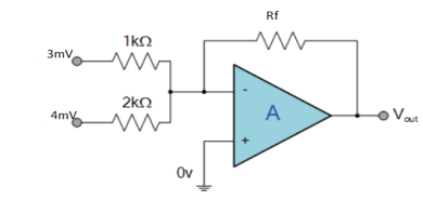
Solution:
We know,
Gain (Av) = =
= 
Hence,
Av1 = 
Av2 = 
Now, Output voltage Vo = Sum of the two amplified input signals
Vo = Av1 x V1 + Av2 x V2
Vo =(-5 x 3) + ( -2.5x 4) mV
Vo = -25mV
As the above output voltage is negative hence it is an inverting amplifier.
Non-Inverting
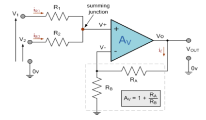
Fig 23: Non-Inverting Summing Amplifier
Applying KCL to the above circuit we have
IR1+IR2 = 0
 =
=  = 0
= 0
When R1 = R2 =R
V+ = 
The voltage gain for non-inverting summing amplifier is given as
AV = Vout/Vin =  = 1+
= 1+
Vout= [1+ ]
] 
Key takeaway
AV = Vout/Vin =  = 1+
= 1+
Vout= [1+ ]
] 
Subtractor
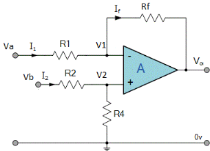
Fig 24: Difference amplifier
- Here input can be provided simultaneously at both the terminals of amplifier.
- Voltage signal Va is applied at one input terminal and another voltage signal Vb onto the other input terminal then resultant output voltage is proportional to the “Difference” between the input voltages Va and Vb.
- Vo = Vb - Va
- Now by applying superposition theorem we get,


Summing point, V1 = V2 and
V2 = Vb
If Vb = 0 then 
And Va = 0 then 
Vo = -V01 + V02
Vo =  +
+ 
If R1 = R2 and Rf = R4 then

And if R1 = R2 = Rf = R4 =R then
Vo = Vb – Va
Hence, is known as a Unity Gain Differential Amplifier.
Key takeaway
The output of subtractor is

Integrator
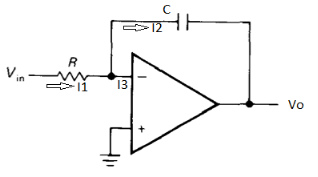
Fig 25: Integrator
- It is a circuit which provides output voltage Vo as an integral form of input voltage Vin.
- It is obtained by using an inverting amplifier and replacing its feedback resistor Rf with a capacitor C.
- Hence,

Ignoring I3 we have, I3 ≈ 0
So, I1 ≈ I2.
- We know current across the capacitor is given by,

- Now by applying Kirchoffs current law,

However, V = 0 because gain A is very large

Integrating both sides we get


 + Q
+ Q
Where Q is the integration constant and is proportional to Vo at t = 0 sec.
Therefore, voltage Vo is directly proportional to Vin and inversely proportional to constant RC.
Frequency response of basic integrator circuit is given by,
 ( for 0 db gain)
Example-1
The integrator circuit as shown in the figure has R = 500K Ω and C=1µF. Find and plot the output voltage for the inputs as shown in the figure.
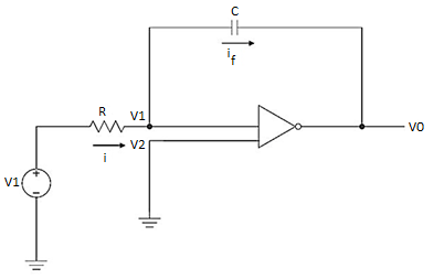
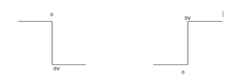
a) b)
c)vi= 2 sin 4tV d) vi= 4tV
Solution:
We know that
v0 = - 1/RC  + v0(0)
Here R= 500K Ω and C = 1µF
1/RC = 1/ 500 x 1000 x 1 x 10-6
= 1/RC = 2
= -2  ; vi =- 5V
= -2 
= 10t V
Which means it is a ramp voltage with positive slopeZ
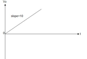
When vi=5V
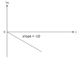
-2  ; vi = 5V
= -2 
= -10t V
Which means it is a ramp voltage with negative slope.
When vi= 2 sin4t V
Vo = -2 
= -4 [-cos 4t] /4 = cos 4t
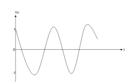
When vi=4t V
Vo = 
= -8 [t2/2] = - 4V
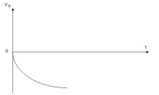
Key takeaway
 + Q
+ Q
Where Q is the integration constant and is proportional to Vo at t = 0 sec.
Differentiator
- A differentiator is a circuit that performs differentiation operation. Hence, the output is a derivative of input.
- In an inverting amplifier, if input resistor is replaced by a capacitor, then a differentiator circuit is formed.
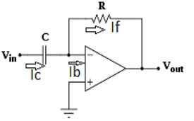
Fig 26: Differentiator
- In the above fig. On applying Kirchhoff’s law we get,

Since Ib = 0 then,
Ic ≈ If

Since Gain A is very large hence, V1 = 0

Or 
- So, the output voltage is RC times the negative rate of change of input voltage.
- When input is a cosine wave, output is a sine wave i.e it performs the inverse function of integrator circuit.
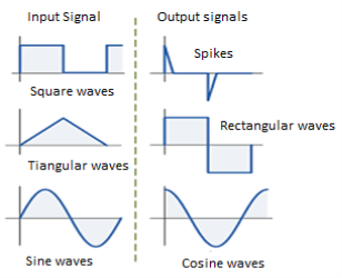
Fig 27: Input and output waveform of differentiator
Frequency response of basic differentiator circuit is given by,
 ( for 0 db gain)
Comparators
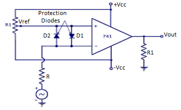
Fig 28 Comparator
- A reference voltage Vref of 1V is applied to the inverting terminal of op-amp.
- A time varying voltage Vin is applied to the non-inverting terminal of op-amp.
- Diode D1 and D2 are used to protect the op-amp from damage from excess amount of input voltage Vin.
- They are known as clamp diodes as they clamp the difference input voltage to +0.7V to -0.7V.
- Hence, the above circuit is called as non-inverting Comparator.
Characteristics of comparator
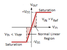
Fig 29 Voltage levels for comparator
- When Vin <Vref , then output Vo = -Vsat (≈ -Vee) because the voltage at negative input is higher than that of positive input.
- When Vin >Vref , then output Vo = +Vsat (≈ +Vee) as the positive input becomes positive with respect to the negative input.
- When Vin ≈ Vref, then Vo changes from one Vsat level to another.
- Therefore the comparator is a type of analog to digital converter.
- It is also known as Voltage Level Detector because for a particular value of Vref , the voltage level of Vin can be detected.
Key takeaway
- When Vin <Vref, then output Vo = -Vsat (≈ -Vee) because the voltage at negative input is higher than that of positive input.
- When Vin >Vref, then output Vo = +Vsat (≈ +Vee) as the positive input becomes positive with respect to the negative input.
Zero Crossing Detector
An op-amp detector that has the ability to detect the change from positive to negative or negative to a positive level of a sinusoidal waveform is known as a zero- crossing detector.
It is also known to be a square wave generator as the applied input signal is converted into a square wave by the zero -crossing detector.
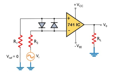
Fig 30 Zero crossing Detector
Here, the input signal Vi is provided to the inverting terminal of the op-amp while the non-inverting terminal is grounded by making use of two resistors R1 and R2.
It detects the point where the input signal crosses zero of the reference voltage level. For every crossing, the saturation level of the output signal changes from one to another.
The reference level is set at 0 and applied at the non-inverting terminal of the op-amp. The sine wave applied at the inverting terminal of the op-amp is compared with the reference level each time the phase of the wave changes either from positive to negative or negative to positive.
Firstly, when positive half of the sinusoidal signal appears at the input. Then the op-amp comparator compares the reference voltage level with the peak level of the applied signal.
Vo = Vref – Vi ---------------------------------------(1)
And we know the reference level is 0, thus
Vo = 0 – ( + Vsat) ----------------------------------------(2)
Therefore, Vo = - Vsat ---------------------------------(3)
During the negative half of the signal, thus the peak will have a negative polarity.
Again
Vo = Vref – Vi ---------------------------------------------(4)
Thus,
Vo = 0 - ( - Vsat) --------------------------------------------------(5)
So, we get
Vo = + Vsat ---------------------------------------------(6)
In this way, the zero -crossing detector detects the change in the level of the applied signal.
Zero crossing detector is also known to be a square wave generator. As the output of the window comparator is nothing but a square wave.
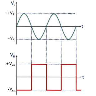
Fig 31 Input and output of zero crossing detector
V0 for the positive half of the applied signal is – Vsat,
This is the reason why we have achieved negative half of the square wave at the output when positive half of the sinusoidal signal is applied. While V0 for the negative half of the sinusoidal signal is + Vsat,
Applications:
- Phase Locked Loop
- Frequency counters and phase meters
Key takeaways
An op-amp detector that has the ability to detect the change from positive to negative or negative to a positive level of a sinusoidal waveform is known as a zero- crossing detector.
Window detector
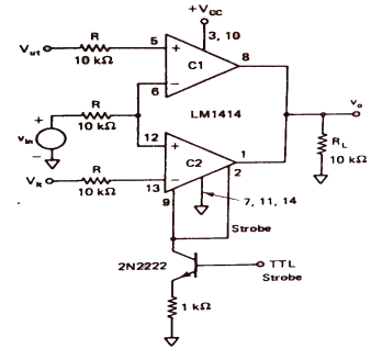
Fig 32 Window Detector using LM1414(Ref 5)
The window detectors are used when we need to calculate an unknown value which is not lying between the two precise reference threshold values Vut and Vlt. As we can see from the above figure that voltage Vin is applied to the inverting end of comparator C1 and non-inverting end to C2.
TO the + input of C1upper threshold voltage Vut is applied and lower threshold voltage Vlt is applied to the – input of C2. When the value of Vin is in between Vut and Vlt the output is high. The output is low when Vin is above Vut or lower then Vlt.
They are usually used in industrial alarms, level detectors and controls, digital computers.
Schmitt trigger
The Schmitt Trigger is a logic input type that provides hysteresis or two different threshold voltage levels for rising and falling edge. This is useful because it can avoid the errors when we have noisy input signals from which we want to get square wave signals.
Symmetrical
If we add a positive feedback by connecting the output voltage to the non-inverting input with a resistor between them and another resistor between the VIN and the non-inverting input we will get the Schmitt Trigger. Now the output will switch from VCC– to VCC+ when the voltage at the A node will cross 0 volts.
That means that now by adjusting the values of the resistors we can set at what value of the VIN input the switch will occur using the following equations. We get these equations with the following relationships. The current “i” through this line equals VIN – VA divided by R1 as well as VA – VOUT divided by R2. So if we replace the VA with zero, as we need that value for the switch to occur, we will get that final equation.
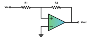
Fig 33 Symmetrical

Va = 0


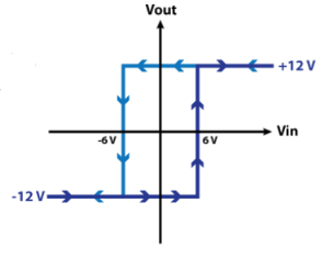
Fig 34 Symmetrical characteristics
Asymmetrical
In order to get two different non-symmetrical thresholds, we can use this circuit of an inverting single powered Schmitt Trigger. Here the VREF voltage is the same as the VCC of the op-amp. Now because the VIN input is connected to the inverting input of the op-amp when its values will reach the upper threshold, the output will switch off to 0 volts, and then when its values will decline to the lower threshold, the output will switch on to 5 volts.
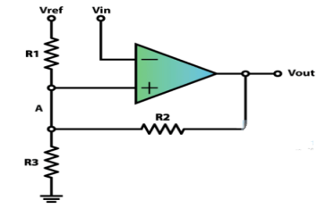
Fig 35 Asymmetrical
Example-1
The VREF = VCC = 5 volts and the three resistors will be the same 10k ohms. So calculate the voltage at the A node. Assume Vout =0V and 5V.
Solution:

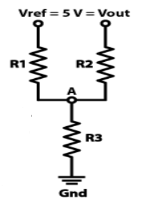
Vout = 0V

Va = 166V
Vout = 5V

Va = 333V
Key takeaway
The Schmitt Trigger is a logic input type that provides hysteresis or two different threshold voltage levels for rising and falling edge. This is useful because it can avoid the errors when we have noisy input signals from which we want to get square wave signals.
Peak detector
Rectifier circuit gives average value of input signal; but in practice we need peak value of input signal. This is achieved by peak detector circuit. The following figure shows a simple peak detector circuit using diode and capacitor.
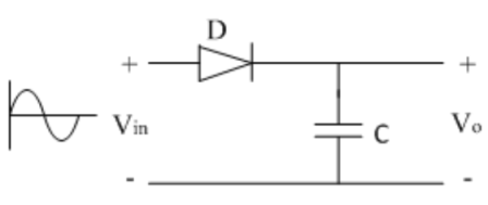
Fig 36 Peak detector
In the positive half cycle, diode D is forward biased and capacitor C starts charging. When input reaches its peak value, capacitor gets charged to positive peak value.
In negative half cycle, as input decreases, diode D is reversed biased and capacitor is isolated and holds the peak value of previous cycle. Hence called as peak detector.
But in practice, output is taken across some load RL, so when input voltage decreases capacitor discharges through load RL. To avoid this, select RL of very large value so that capacitor discharges very slowly hence almost hold the charge. Whatever charge it lost through RL is gets back in next half cycle.
Key takeaway
The diode D is acting as an instant switch, so supply gets loaded.
To avoid the loading while charging capacitor, we use op-amp.
Log Amplifier
As the name says it is an amplifier which produces the output proportional to logarithmic of the applied input. The log amplifier using op-amp is shown below. The input is applied through the inverting end of op-amp. As the non-inverting end has voltage zero then by virtual ground concept the voltage at inverting terminal also becomes zero.
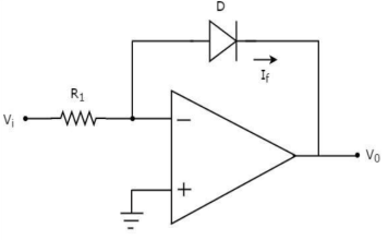
Fig 37 Log Amplifier
The equation for input voltage will be
 +If = 0
If = 
The current flowing through diode is given as

Where:
Is = Saturation Current
Vf = Voltage drop across diode in forward bias
VT = Thermal equivalent voltage
For feedback loop the KVL equation will be
0-Vf -V0 = 0
Vf = -V0
Substituting Vf in above equation of If

Equating both equations of If
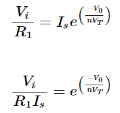
Taking natural log of both sides we get

The above equations shows that the output is natural log of the applied input.
Antilog Amplifier
This device produces the output proportional to antilog of input. The inverting op-amp is used in this case as well. The figure below shows an antilog amplifier with its inverting terminal connected to the input end with diode and the non-inverting terminal is grounded.
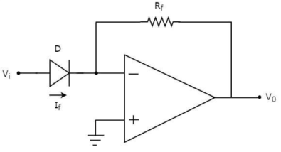
Fig 38 Antilog Amplifier
Applying KCL at input terminal we get


The current flowing through diode is given as

Substituting If in above voltage equation we get


At inverting terminal applying KVL we get


Substituting Vf in equation of V0 we get

The above equations shows that the output is natural antilog of the applied input.
Key takeaways
For Log Amplifier

For Antilog Amplifier

Precision rectifier
The major limitation of conventional rectifiers is that it cannot rectify AC voltages below forward voltage drop VD (0.7V) of a diode. The precision rectifier will make it possible to rectify input voltage of a very small magnitude even less than forward voltage drop of diode. The diode can be used in AM detector where power is negligible and we want information in the signal. Rectifier circuits used for circuit detection with op-amps are called precision rectifiers.
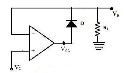
Fig 39 Precision Rectifier
The below figure shows a non-inverting precision rectifier. The diode used is called as precision diode. When the voltage VI is positive the voltage VOA is also positive. When Vi<0the voltage VOA becomes negative and hence reverse biasing the diode and making Vo =0.
When the value of input voltage Vi< (cut-in voltage). The diode again becomes reverse biased as VOA becomes negative. The op-amp then comes to negative saturation. There is no current through RL and V0= 0.
When the value of input voltage Vi> (cut-in voltage) the circuit acts as voltage follower and the output voltage follows the input voltage during this positive half cycle of input.
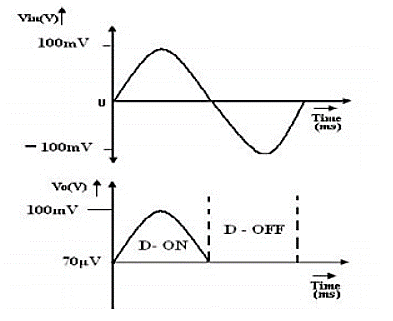
Fig 40 Input and Output of Precision Rectifier
The precision rectifier is another rectifier that converts AC to DC, but in a precision rectifier we use an op-amp to compensate for the voltage drop across the diode, that is why we are not losing the 0.6V or 0.7V voltage drop across the diode, also the circuit can be constructed to have some gain at the output of the amplifier as well.
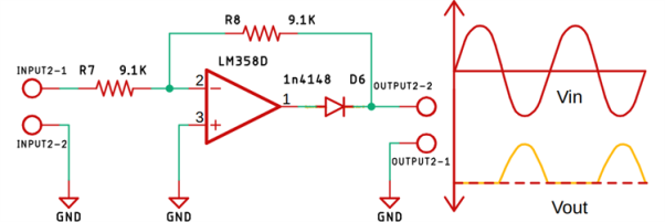
Fig 41 Half wave precision rectifier circuit.
The input and output waveform of the precision rectifier circuit, which is exactly equal to the input. That's because we are taking the feedback from the output of the diode and the op-amp compensates for any voltage drop across the diode. So, the diode behaves like an ideal diode.
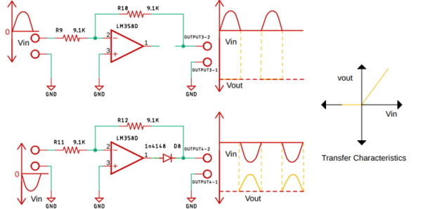
Fig 42 When positive and negative half cycle of input signal is applied to Op-amp
Full wave precision rectifier circuit
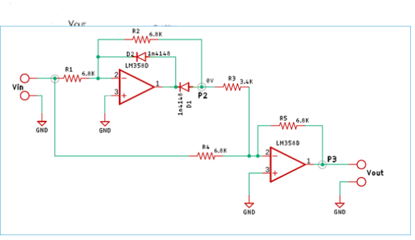
Fig 43 Full wave Precision circuit
In full wave summing amplifier is added at the output. From the point, P1 to point P2 is the basic precision rectifier circuit and the diode is so configured that we get a negative voltage at the output.
From the point, P2 to point P3 is the summing amplifier, the output from the precision rectifier is fed to the summing amplifier through the resistor R3.
The input from the point P1 is also fed to the summing amplifier with the help of the resistor R4, the resistors R4 and R5 are responsible for setting the gain of the op-amp to 1X.
Since the output from the Point P2 is fed directly to the summing amplifier with the gain of 2X, that means the output voltage will be 2-times the input voltage. The output is obtained at P3.
Key takeaway
The precision diode operates in first quadrant when Vi>0 and V0>0. The precision diode operates in third quadrant when diode is connected in reverse bias.
Introduction to modulation
- It is a process through which audio, video, image or text information is added to an electrical or optical carrier signal that is to be transmitted over a telecommunication or electronic medium.
- It enables the transfer of information on an electrical signal to a receiver that is capable of demodulating the signal to extract the blended information.
- It is primarily used in telecommunication technologies that require the transmission of data via electrical signals.
- It is considered the backbone of data communication as it enables the use of electrical and optical signals as information carriers.
- This is done by altering the periodic waveform or the carrier.
- This comprises of its amplitude, frequency and phase.
- Modulation has three different types:
- Amplitude Modulation (AM): Amplitude of the carrier is modulated.
- Frequency Modulation (FM): Frequency of the carrier is modulated.
- Phase Modulation (PM): Phase of the carrier is modulated.
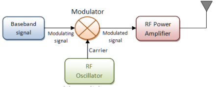
Fig.44: Modulation
Demodulation (downward frequency translation)
- It is the process of extracting the original information-carrying signal from a modulated carrier wave.
- A demodulator is an electronic circuit that is mainly used to recover the information from the modulated carrier wave.
- There are different types of demodulators.
- The output signal via demodulator may be sound, images or binary data.
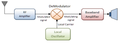
Fig.45: Demodulation
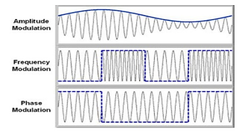
Fig.46: Demodulated Output
Necessity of Modulation: -
1>. Antenna height reduces
2>. Avoids mixing of signal
3>. Increases the range of communication [ In Kilometres]
4>. Multiplexing of signals is possible
5>. Improves quality of reception of signal.
1>. Antenna height Reduces: - Antenna theory specifies that the height of the antenna required for radiation of radio waves is a function of wavelength of the frequency fed at the i/p of the antenna. Antenna height must be multiple of ( d/4 ),
Where ‘ d ‘ is the wavelength.
d = speed of light / frequency of signal
d = c / f = 3 x 10⁸ / f
Eg : Consider the voice as analog baseband signal with f = 4 KHz
d = 3 x 10⁸ / 4 x 10³
d = 75 x 103 m
d = 75 km
Height of antenna required is d / 4
= 75 km / 4 = 18.75 km
Q. Practically you cannot build the antenna of 18.7 km height. Consider this voice signal of 4 kHz frequency is used to modulate the carrier signal of 2 MHz frequency.
F = 2 MHz
D = c / f = 3 x 10⁸ / 2 x 106 = 150 m
Minimum height of antenna required = d / 4 = 150 / 4 = 37.5 m
Therefore, antenna height required for radio communication reduces from 75 km to 37.5 meters due to modulation.
2>. Increase range of communication: - The frequency of baseband signal is low. At low frequency the signal radiation from antenna is poor or weak. Due to this reason the signal gets attenuated and can’t travel long distance when it is transmitted.
Attenuation of the transmitted signal reduces when the frequency is increased.
Thus modulation increases the frequency of the signal to be radiated. Thus, increase in frequency increases the range of communication.
Key Takeaways:
- Modulation increases the frequency of the signal to be radiated.
- Antenna height must be multiple of ( d/4 ).
- Demodulation is the process of extracting the original information-carrying signal from a modulated carrier wave.
- Modulation is a process through which audio, video, image or text information is added to an electrical or optical carrier signal that is to be transmitted over a telecommunication or electronic medium.
Amplitude Modulation (AM)
The amplitude of the carrier signal varies in accordance with the instantaneous amplitude of the modulating signal. That is the amplitude of the carrier signal containing no information varies as per the amplitude of the signal containing information, at each instant.
Consider the following diagram
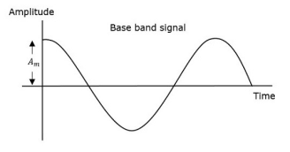
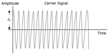
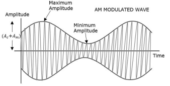
Fig.47: Amplitude Modulation
The first figure shows the modulating wave, which is the message signal. The next one is the carrier wave, which is a high frequency signal and contains no information. While, the last one is the resultant modulated wave.
It can be observed that the positive and negative peaks of the carrier wave are interconnected with an imaginary line. This line helps recreating the exact shape of the modulating signal. This imaginary line on the carrier wave is called as Envelope. It is the same as that of the message signal.
Therefore, we can say that Amplitude Modulation is the process of changing the amplitude of a relatively high frequency carrier signal in accordance with the amplitude of the modulating signal (Information). The carrier amplitude varies linearly by the modulating signal which usually consists of a range of audio frequencies. The frequency of the carrier is not affected.
The various forms of Amplitude Modulation are:
- Conventional Amplitude Modulation Full AM or Double Sideband Large carrier modulation (DSBLC) /Double Sideband Full Carrier (DSBFC)
- Double Sideband Suppressed carrier (DSBSC) modulation.
- Single Sideband (SSB) modulation
Generation of double side band (DSB) with carrier
DSBFC (Double Side Band Full Wave Carrier)
Time-Domain Representation
Let the modulating signal be,
m(t)=Am cos (2πfmt) --------------(1)
And the carrier signal be,
c(t)=Ac cos(2πfct) c(t) ---------------(2)
Where, Am and Ac are the amplitude of the modulating signal and the carrier signal respectively.
fm and fc are the frequency of the modulating signal and the carrier signal respectively.
Then, the equation of Amplitude Modulated wave will be
s(t)= [Ac+ Am cos(2πfmt)] cos(2πfct) -------------------------- (3)
s(t) = [ Ac cos(2πfct) + Ac Am cos(2πfmt). Cos(2πfct] ---------(4)
s(t) = Ac [1 + Am/Ac cos(2πfmt)] cos(2πfct) ----------- (5)
Here the modulation index µ = Am/Ac.
s(t) = Ac [1 + µ cos(2πfmt)] cos(2πfct) -------------- (6)
Modulation index
Let Amax and Amin be the maximum and minimum amplitudes of the modulated wave.
We will get the maximum amplitude of the modulated wave, when cos(2πfmt)
Is 1.
That is Amax=Ac + Am
We will get the minimum amplitude of the modulated wave, when cos(2πfmt)
Is -1.
That is Amin = Ac - Am
Amax + Amin = Ac + Am + Ac –Am = 2Ac
Ac = Amax + Amin/2
Similarly,
Amax – Amin = Ac + Am – Ac +Am = 2Am
Am = Amax – Amin /2
Therefore
µ = Amax + Amin
Amax - Amin
Bandwidth:
Bandwidth is the difference between the highest and lowest frequencies of the signal.
BW = fmax – fmin
s(t) = Ac [1+ μ cos(2πfmt)] cos(2πfct)
s(t) = Ac cos(2πfct) + Ac μ cos(2πfmt) cos(2πfct)
s(t) = Ac cos(2πfct) + Ac μ/2 cos 2π (fc + fm) t + Ac μ/2 cos 2π (fc - fm) t
Hence, the amplitude modulated wave has three frequencies.
- Carrier frequency fc
- Upper sideband frequency fc+fm
- And lower sideband frequency fc−fm
Here, fmax=fc+fm and fmin=fc−fm
BW=fc+fm−(fc−fm)
BW=fc+fm−(fc−fm)
BW= 2fm
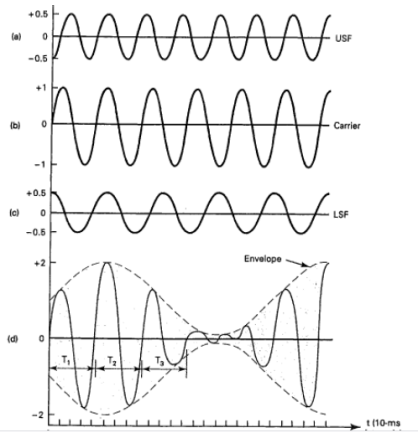
Fig.48: DSBFC
Power Calculation of AM
Consider the following equation of amplitude modulated wave.
s(t)=Ac cos(2πfct)+Acμ 2 cos[2π(fc+fm)t]+ Acμ 2cos[2π(fc−fm)t] -------(1)
Power of AM wave is equal to the sum of powers of carrier, upper sideband, and lower sideband frequency components.
Pt=Pc+ PUSB+ PLSB
We know that the standard formula for power is
P = vrms 2 / R = (vm /  ) 2 /2
Where,
Vrms is the rms value of cos signal.
Vm is the peak value of cos signal.
The powers of the carrier, the upper and lower sideband is given by
Carrier power
Pc=(Ac/√2)2/R=Ac2/2R
Upper sideband power
PUSB=(Acμ/2√2)2/R= Ac2 μ2/ 8R
Similarly, for lower sideband power same as that of the upper side band power.
PLSB=(Acμ/2√2)2 /R
PLSB=Ac2μ2/R
Now, let us add these three powers in order to get the power of AM wave.
Pt=Ac2 /2R+Ac2μ2 /8R+Ac2μ2/8R
Pt= Ac2 /2R[ 1+μ2 /4+μ2 /4]
Pt=Pc ( 1+ μ 2/2 )
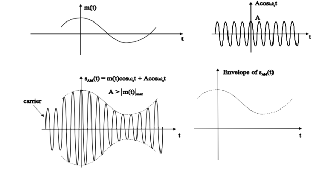
Fig.49: DSBFC
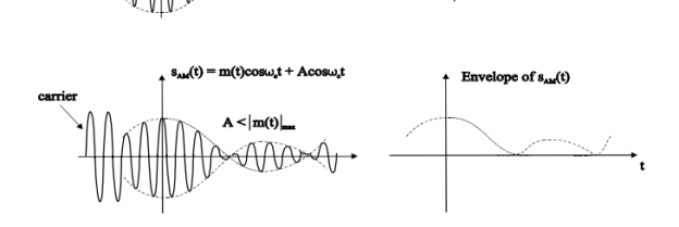
Fig.50: DSBFC
Problems
A modulating signal m(t)=10cos(2π×103t) m(t) is amplitude modulated with a carrier signal c(t)=50cos(2π×105t). Find the modulation index, the carrier power, and the power required for transmitting AM wave.
Solution
Given, the equation of modulating signal as
m(t)=10 cos(2π×103t) m(t)
We know the standard equation of modulating signal as
m(t)=Am cos(2πfmt) m(t)
By comparing the above two equations, we will get
Am=10 volts
And Frequency of modulating signal as
Fm=103Hz=1KHz
Given, the equation of carrier signal is
c(t)=50 cos(2π×105t))
The standard equation of carrier signal is
c(t)=Ac cos(2πfct) c(t)
By comparing these two equations, we will get
Amplitude of carrier signal as Ac=50 volts
And Frequency of carrier signal as fc=105Hz=100KHz
We know the formula for modulation index as
μ=Am/Ac
μ=10/50=0.2
Therefore, the value of modulation index is 0.2 and percentage of modulation is 20%.
The formula for Carrier power, Pc
Pc=Ac2 /2R
Assume R=1ΩR=1Ω and substitute Ac value in the above formula.
Pc=(50)2/2(1)=1250W
Therefore, the Carrier power, Pc is 1250 watts.
We know the formula for power required for transmitting AM wave is
Pt=Pc(1+μ2/2)
Pt=1250(1+(0.2)22)=1275W
Therefore, the power required for transmitting AM wave is 1275 watts.
Key Takeaways:
- Power of AM wave is equal to the sum of powers of carrier, upper sideband, and lower sideband frequency components.
Pt=Pc+ PUSB+ PLSB
2. Bandwidth is the difference between the highest and lowest frequencies of the signal.
BW = fmax – fmin
3. Modulation index is given by µ = Amax + Amin
Amax – Amin
Double side band with suppressed carrier (DSB-SC) and Single side band with suppressed carrier
DSBSC (Double Side Band Suppressed Carrier)
In DSBC modulation, the modulated wave consists of only the upper and lower side bands. Transmitted power is saved through the suppression of the carrier wave, but the channel bandwidth requirement is the same.
DSBSC modulators make use of the multiplying action in which the modulating signal multiplies the carrier wave. In this system, the carrier component is eliminated and both upper and lower side bands are transmitted. As the carrier component is suppressed, the power required for transmission is less than that of AM.
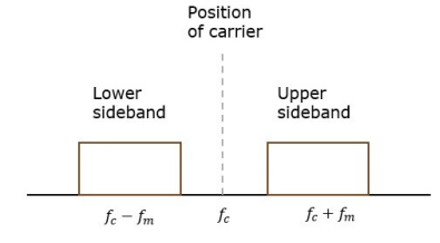
Fig.51: Position of carrier
Carrier is suppressed and base band is allowed for transmission.
If m(t) = Am cos(2πfmt) is the modulating signal and c(t) = Ac cos(2πfct) is the carrier signal then DSBSC wave s(t) is given by
s(t) = c(t) m(t) ------------------- (1)
s(t) =Am cos(2πfmt) Ac cos(2πfct) -------- (2)
s(t) = Am Ac cos(2πfmt) cos(2πfct) ------- (3)
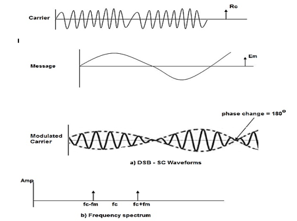
Fig.52: DSBSC
The figure shows the waveform and the frequency spectrum.
The envelope of a DSBSC modulated signal is therefore different from the message signal and the Fourier transform of s(t) is given by
S(f) = Ac/2[ M(f-fc) + M(f + fc)]
When base band signal m(t) is limited to interval –W<fc<W we find the spectrum S(f) of the DSBSC wave s(t) as shown in the figure. We see that there is a change in the scaling factor , the modulation process translates the spectrum of the base band signal by fc. The transmission bandwidth is same as AM.
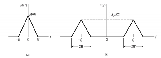
Fig.53: DSBSC transmission bandwidth
Bandwidth of DSBSC Wave
We know the formula for bandwidth (BW) is
BW=fmax−fmin
Consider the equation of DSBSC modulated wave.
s(t)=AmAccos(2πfmt)cos(2πfct)s(t)
s(t)=AmAc2cos[2π(fc+fm)t]+AmAc2cos[2π(fc−fm)t]
The DSBSC modulated wave has only two frequencies. So, the maximum and minimum frequencies are fc+ fm and fc− fm respectively.
i.e.,fmax=fc+fm and fmin=fc−fm
BW=fc+fm−(fc−fm)
BW = 2fm
Thus, the bandwidth of DSBSC wave is same as that of AM wave and it is equal to twice the frequency of the modulating signal.
Power of DSBSC Wave
Consider the following equation of DSBSC modulated wave.
s(t)=AmAc2cos[2π(fc+fm)t]+AmAc2cos[2π(fc−fm)t]
Power of DSBSC wave is equal to the sum of powers of upper sideband and lower sideband frequency components.
Pt=PUSB+PLSB
We know the standard formula for power of cos signal is
P=vrms2 /R=(vm√2)2 /R
First, let us find the powers of upper sideband and lower sideband one by one.
Upper sideband power
PUSB=(AmAc/2√2)2/R=Am2Ac2 / 8R
Similarly, we will get the lower sideband power same as that of upper sideband power.
PLSB=Am2Ac2/8R
Now, let us add these two sideband powers in order to get the power of DSBSC wave.
Pt=Am2Ac2 /8R+Am2Ac2/8R
Pt=Am2Ac2 /4R
Therefore, the power required for transmitting DSBSC wave is equal to the power of both the sidebands.
Generation of DSBSC Waves:
Balanced Modulator (Product Modulator)
A balanced modulator consists of two standard amplitude modulators arranged in a balanced configuration so as to suppress the carrier wave as shown in the following block diagram. It is assumed that the AM modulators are identical, except for the sign reversal of the modulating wave applied to the input of one of them. Thus, the output of the two modulators may be expressed as,
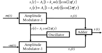
Fig.54: Balanced Modulator
Subtracting s2(t) from s1(t) we get
s(t) = s1(t) – s2(t)
s(t) = 2 ka m(t) cos(2πfct)
Hence, except for the scaling factor 2ka, the balanced modulator output is equal to the product of the modulating wave and the carrier.
Ring Modulator
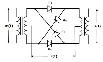
Fig.55: Ring Modulator
Operation
- In this diagram, the four diodes D1,D2,D3 and D4 are connected in the ring structure. Hence, this modulator is called as the ring modulator.
- Two center tapped transformers are used in this diagram. The message signal m(t) is applied to the input transformer, whereas, the carrier signals c(t) is applied between the two center tapped transformers.
- During the positive half cycle of the carrier signal, the diodes D1 and D3 are switched ON and the other two diodes D2 and D4 are switched OFF.
- In this case, the message signal is multiplied by +1.
- During the negative half cycle of the carrier signal, the diodes D2 and D4 are switched ON and the other two diodes D1 and D3 are switched OFF.
- In this case, the message signal is multiplied by -1. This results in 1800 phase shift in the resulting DSBSC wave.
From the above analysis, we can say that the four diodes D1, D2, D3 and D4 are controlled by the carrier signal.
If the carrier is a square wave, then the Fourier series representation of c(t) is given by
c(t) = 4 / π  n-1 / 2n -1 cos[2πfct(2n−1)]
We will get DSBSC wave s(t) which is just the product of the carrier signal c(t)) and the message signal m(t) i.e.,
s(t) = 4 / π  n-1 / 2n -1 cos[2πfct(2n−1)] m(t)
The ring modulator.
DSBSC modulators are known as product modulators as they produce the output, which is the product of two input signals.
Balanced Modulator using Non-linear resistance
- The DSBSC generation using balanced modulator based on nonlinear resistance characteristics of diode is shown in the figure below.
- The diode in the balanced modulator use the nonlinear resistance property for producing modulated signals.
- Carrier voltage is applied in phase at both the diodes, while modulating voltage appears 180° out of phase at the diode inputs as they are at opposite ends of a center- tapped transformer.
- The modulated output currents of the two diodes are combined in the center tapped primary of the output transformer, which then gets subtracted.
- The output of the balanced modulator contains two sidebands and sum of the harmonic components.
As indicated in the Figure, the input voltage at diode D1 is vc+vm and input voltage at diode D2 is vc−vm.
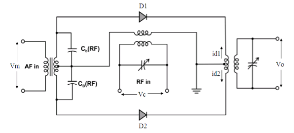
Fig.56: Balanced Modulator using Non-linear resistance
The primary current of the output transformer is i1=id1−id2.
Where:
Id1=a+ b(vc+vm) + c(vc+vm)2
Id2=a+ b(vc−vm) +c(vc−vm)2
Thus, we get,
i1= id1−id2=2bvm+4cvmvc
The modulating and carrier voltage are represented as,
vm=Vmsinωmt and vc=Vcsinωct
Substituting for vm and vc and simplifying, we get,
i1=2bVmsinωmt+4cmVc/2cos(ωc−ωm)t−4cmVc/2cos(ωc+ωm)t
The output voltage v0 is proportional to primary current i1 and assume constant of proportionality as α, which can be expressed as,
v0=αi1=2αbVmsinωmt+4αcmVc/2cos(ωc−ωm)t−4αcmVc/2cos(ωc+ωm)t
Let P=2αbVmP and Q=2αcmVc2.
Thus we have,
v0=Psinωmt+2Qcos(ωc−ωm)t−2Qcos(ωc+ωm)t
The above equation shows that carrier has been cancelled out, leaving only two
Sidebands and the modulating frequencies from the output is eliminated by the tuning of the output transformer, which results in the below equation of the generated DSBSC wave.
v0=2Qcos(ωc−ωm)t−2Qcos(ωc+ωm)t
Switching Modulator
.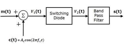
Fig.57 Switching Modulator
Switching modulator is similar to the square law modulator. The only difference is that in the square law modulator, the diode is operated in a non-linear mode, whereas, in the switching modulator, the diode has to operate as an ideal switch.
Let the modulating and carrier signals be denoted as m(t) and c(t)=Accos(2πfct). These two signals are applied as inputs to the summer (adder) block. Summer block produces an output, which is the addition of modulating and carrier signals. Mathematically, we can write it as
V1(t)=m(t)+c(t)=m(t)+Accos(2πfct)
This signal V1(t) is applied as an input of diode.
Assume, the magnitude of the modulating signal is very small when compared to the amplitude of carrier signal Ac. So, the diode’s ON and OFF action is controlled by carrier signal c(t). This means, the diode will be forward biased when c(t)>0 and it will be reverse biased when c(t)<0.
Therefore, the output of the diode is
V2(t)={V1(t)0 if c(t)>0
0 c(t) <0
We can approximate this as
V2(t)=V1(t)x(t)
Where, x(t) is a periodic pulse train with time period T=1fc

The Fourier series representation of this periodic pulse train is
x(t)=1/ 2+2π  n -1 / 2n-1 cos( 2π(2n-1) fc(t))---------------------(1)
= ½ + 2/π cos(2πfct) -2 / 3 π cos(6πfct)+ ………… ----------------(2)
Substituting V1(t) and x(t) we get
V2(t) = [m(t) + Ac cos(2πfct) ] [½ + 2/π cos(2πfct) -2 / 3 π cos(6πfct)+ …………]---------------------------------------(3)
V2(t) = Ac/2 (1+ 4/πAc)m(t) cos(2πfct) + m(t)/2 + 2Ac/π cos (2πfct)- 2m(t)/3π cos(6 πfct)- 2A/3π cos(2πfct) cos(6πfct) + ………………………….
The 1st term of the above equation represents the desired AM wave and the remaining terms are unwanted terms. Thus, with the help of band pass filter, we can pass only AM wave and eliminate the remaining terms.
Therefore, the output of switching modulator is
s(t)=Ac2(1+(4π/Ac)m(t))cos(2πfct)
We know the standard equation of AM wave is
s(t)=Ac[1+kam(t)]cos(2πfct)s(t)
Where, ka is the amplitude sensitivity.
By comparing the output of the switching modulator with the standard equation of AM wave, we will get the scaling factor as 0.5 and amplitude sensitivity ka as 4π/Ac.
SSB-SC
The process of suppressing one of the sidebands along with the carrier and transmitting a single sideband is called as Single Sideband Suppressed Carrier system or simply SSBSC. It is plotted as shown in the following figure.
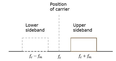
Fig.58 SSB
Carrier and sideband are suppressed and single sideband is allowed for transmission.
Let us consider the
Modulating signal
m(t)=Amcos(2πfmt)
Carrier signal
c(t)=Accos(2πfct)
Mathematically, we can represent the equation of SSB-SC wave as
s(t)=AmAc2cos[2π(fc+fm)t] for the upper sideband
Or
s(t)= AmAc2cos[2π(fc−fm)t] for the lower sideband
Bandwidth of SSB-SC Wave
We know that the DSB-SC modulated wave contains two sidebands and its bandwidth is 2fm. Since the SSB-SC modulated wave contains only one sideband, its bandwidth is half of the bandwidth of DSBSC modulated wave.
i.e., Bandwidth of SSBSC modulated wave =2fm/2=fm
Therefore, the bandwidth of SSB-SC modulated wave is fm and it is equal to the frequency of the modulating signal.
Power Calculations of SSB-SC Wave
Consider the following equation of SSBSC modulated wave.
s(t)=AmAc/2 cos[2π(fc+fm)t] for the upper sideband
Or
s(t)=AmAc/2 cos[2π(fc−fm)t] for the lower sideband
Power of SSB-SC wave is equal to the power of any one sideband frequency components.
Pt=PUSB=PLSB
We know power
P=vrms2 / R
=(vm/√2)2 / R
In this case, the power of the upper sideband is
PUSB=(AmAc/2√2)2 / R = Am2Ac2 /8R.
Similarly, for lower sideband power.
PLSB=Am2Ac2 / 8R
Therefore, the power of SSB-SC wave is
Pt=Am2Ac2 / 8R
Advantages
- Bandwidth or spectrum space occupied is lesser than AM and DSBSC waves.
- Transmission of more number of signals is allowed.
- Power is saved.
- High power signal can be transmitted.
- Less amount of noise is present.
- Signal fading is less likely to occur.
Disadvantages
- The generation and detection of SSBSC wave is a complex process.
- The quality of the signal gets affected unless the SSB transmitter and receiver have an excellent frequency stability.
Applications
- Power saving requirements and low bandwidth requirements.
- In land, air, and maritime mobile communications.
- Point-to-point communications.
- Radio communications.
- Television, telemetry, and radar communications.
- Military communications, such as amateur radio, etc.
Generation of SSB-SC
We can generate SSBSC wave using the following two methods.
- Frequency discrimination method
- Phase discrimination method
Frequency Discrimination Method
In this method the DSB signal is passed through band pass filter to generate SSB signal.
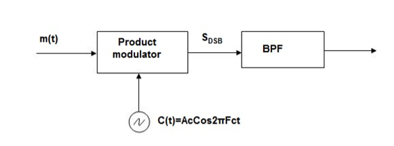
Fig.59 Frequency Discrimination method
The center frequency of the band pass signal decides whether USB or LSB signal is generated.
Suppose we want to transmit USB then using band pass filter with center frequency fc + w/2 we obtain the desired result as shown in the figure.
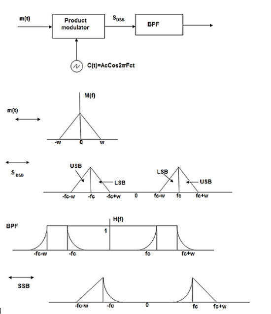
Fig.60: Resultant output
Phase Discriminated Method:
Consider the following block diagram of SSB-SC modulator using phase discrimination method.
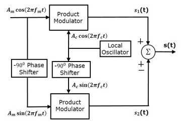
Fig.61 Phase Discriminated Method
- It consists of two product modulators, two −900 phase shifters, one local oscillator and one summer block.
- The product modulator produces an output, which is the product of two inputs.
- The −900 phase shifter produces an output, which has a phase lag of −900 with respect to the input.
- The local oscillator is used to generate the carrier signal.
- Summer block produces an output, which is either the sum of two inputs or the difference of two inputs based on the polarity of inputs.
The modulating signal
m(t) = Amcos(2πfmt) -----------------(1)
The carrier signal
c(t) = Accos(2πfct) -----------------------(2)
Which are directly applied as inputs to the upper product modulator. So, the upper product modulator produces an output, which is the product of these two inputs.
The output of upper product modulator is
s1(t)=AmAc cos(2πfmt)cos(2πfct) --------------------(3)
s1(t)=AmAc/2{cos[2π(fc+fm)t]+cos[2π(fc−fm)t]} -----------(4)
The modulating signal Am cos(2πfmt) and the carrier signal Ac cos(2πfct) are phase shifted by −900 before applying as inputs to the lower product modulator. So, the lower product modulator produces an output, which is the product of these two inputs.
The output of lower product modulator is
s2(t)=AmAc cos(2πfmt−900)cos(2πfct−900) ---------------(5)
s2(t)=AmAc sin(2πfmt) sin(2πfct) -------------------(6)
s2(t)=AmAc/2{cos[2π(fc−fm)t]−cos[2π(fc+fm)t]} ----------(7)
Add s1(t) and s2(t) in order to get the SSB-SC modulated wave s(t) having a lower sideband.
s(t)=AmAc/2{cos[2π(fc+fm)t]+cos[2π(fc−fm)t]}+AmAc/2{cos[2π(fc−fm)t]−cos[2π(fc+fm)t]} ----------------------------------(8)
s(t)=AmAc cos[2π(fc−fm)t] ------------------------(9)
Subtract s2(t) from s1(t) in order to get the SSBSC modulated wave s(t) having a upper sideband.
s(t)=AmAc/2{cos[2π(fc+fm)t]+cos[2π(fc−fm)t]}−AmAc/2{cos[2π(fc−fm)t]−cos[2π(fc+fm)t]} ---------------------------------------------------------(10)
s(t)=AmAc cos[2π(fc+fm)t] --------------------------(11)
Hence, by properly choosing the polarities of inputs at summer block, we will get SSB-SC wave having a upper sideband or a lower sideband.
Key Takeaways:
- We can generate SSBSC wave using the following two methods.
- Frequency discrimination method
- Phase discrimination method
2. The power of SSB-SC wave is Pt=Am2Ac2 / 8R
3. The process of suppressing one of the sidebands along with the carrier and transmitting a single sideband is called as Single Sideband Suppressed Carrier system or simply SSBSC.
4. The power of DSB-SC wave is Pt=Am2Ac2 /4R
5. In DSBC modulation, the modulated wave consists of only the upper and lower side bands. Transmitted power is saved through the suppression of the carrier wave, but the channel bandwidth requirement is the same.
Angle Modulation
Another type of modulation in continuous-wave modulation is Angle Modulation.
Angle Modulation is the process in which the frequency or the phase of the carrier
Signal varies according to the message signal.
The standard equation of the angle modulated wave is
s(t)=Ac cos θi(t)-------------------(1)
Where:
Ac is the amplitude of the modulated wave, which is the same as the amplitude of the carrier signal
θi(t) is the angle of the modulated wave
Angle modulation is further divided into frequency modulation and phase modulation.
- Frequency Modulation is the process of varying the frequency of the carrier signal linearly with the message signal.
- Phase Modulation is the process of varying the phase of the carrier signal linearly with the message signal.
3. Phase Modulation
In frequency modulation, the frequency of the carrier varies whereas, in Phase Modulation (PM), the phase of the carrier signal varies in accordance with the instantaneous amplitude of the modulating signal.
So, in phase modulation, the amplitude and the frequency of the carrier signal remains constant.
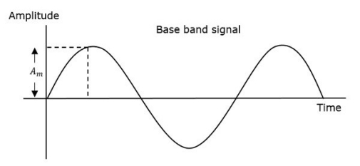
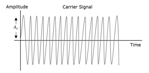
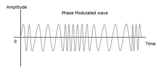
Fig 62 Angle Modulation
The phase of the modulated wave has infinite points, where the phase shift in a wave can take place. The instantaneous amplitude of the modulating signal changes the phase of the carrier signal. When the amplitude is positive, the phase changes in one direction and if the amplitude is negative, the phase changes in the opposite direction.
Representation
The equation for instantaneous phase ϕi in phase modulation is
ϕi=kpm(t)----------------------(1)
Where,
- Kp is the phase sensitivity
- m(t) is the message signal
The standard equation of angle modulated wave is
s(t)=Ac cos(2πfct+ϕi) -------------------------------(2)
Substitute, ϕi value in the above equation.
s(t)=Ac cos(2πfct+kpm(t))-----------------------------------(3)
This is the equation of PM wave.
If the modulating signal,
m(t)=Am cos(2πfmt)--------------------------------(4)
Then the equation of PM wave will be
s(t)=Ac cos(2πfct+βcos(2πfmt))-----------------------------------(5)
Where,
- β = modulation index = Δϕ=kpAm
- Δϕ is phase deviation
Phase modulation is used in mobile communication systems, while frequency modulation is used mainly for FM broadcasting.
Bessel Function and its Mathematical Analysis
Time – Domain Expression:
Since the FM wave is a nonlinear function of the modulating wave, the frequency modulation is a nonlinear process.
Let us consider a single-tone sinusoidal message signal defined by
n(t) = An cos(2nƒnt) -----------------------(1)
The instantaneous frequency is
ƒ(t) = ƒc+kƒAn cos(2nƒnt) -----------------------(2)
= ƒc+∆ƒ cos(2nƒnt)-----------------------------(3)
∆ƒ = kƒAn
 = 2 πfct + 2πKf
  m cos(2 πfmt) dt -------------------(4)
= 2 πfct + 2πKf Am / 2πfm sin(2πfmt) --------------------(5)
= 2 πfct + Kf Am/fm sin(2πfmt) ------------------------(6)
= 2 πfct + β f sin(2πfmt) ---------------------------(7)
Where β = ∆ƒ/fm = Kf Am/fm = modulation index.
Therefore, the single-tone FM wave is expressed by
FM(t) = Ac cos[2nƒct + þƒ sin(2nƒnt)] ------------------------------(8)
This is the desired time-domain expression of the single-tone FM wave
Similarly, single-tone phase modulated wave may be determined where
PM(t) = Ac cos[2nƒct + kp An cos(2nƒnt)] -------------------------(9)
Or, PM(t) = Ac cos[2nƒct +þp cos(2nƒnt)] --------------------------(10)
þp = kpAn ---------------------------(11)
The frequency deviation of the single-tone PM wave is
FM(t) = Ac cos[2 πfct + β f sin(2πfmt)]-----------------(12)
Frequency Modulation
In amplitude modulation, the amplitude of the carrier signal varies, whereas in Frequency Modulation (FM), the frequency of the carrier signal varies in accordance with the instantaneous amplitude of the modulating signal.
Hence, in frequency modulation, the amplitude and the phase of the carrier signal remains constant.
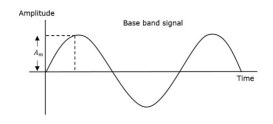
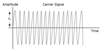
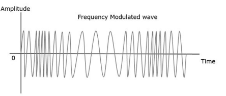
Fig 63 Frequency Modulation
- The frequency fi of the information signal controls the rate at which the carrier frequency increases and decreases. As with AM, fi must be less than fc. The amplitude of the carrier remains constant throughout this process.
- When the information voltage reaches its maximum value then the change in frequency of the carrier will have also reached its maximum deviation above the nominal value.
- Similarly, when the information reaches a minimum, the carrier will be at its lowest frequency below the nominal carrier frequency value.
- When the information signal is zero, then no deviation of the carrier will occur. The maximum change that can occur to the carrier from its base value fc is called the fc. This sets the dynamic range i.e. voltage frequency deviation, of the transmission. The dynamic range is the ratio of the largest and smallest analogue information signals that can be transmitted.
Representation:
The equation for instantaneous frequency fi in FM modulation is
fi=fc+ kf m(t)------------------------(1)
Where:
fc is the carrier frequency
kf is the frequency sensitivity
m(t) is the message signal
We know the relationship between angular frequency ωi and angle θi(t) as
ωi=dθi(t)/dt -------------------------(2)
2πfi=dθi(t)dt-------------------------(3)
θi(t)=2π  i dt -------------------------(4)
Substitute, fi value in the above equation.
θi(t)=2π  +kf m(t) dt-----------------(5)
θi(t)=2πfct+2πkf  (t)dt --------------------(6)
This is the equation of FM wave.
If the modulating signal is m(t)=Am cos(2πfmt) then the equation of FM wave will be
s(t)=Ac cos(2πfct+βsin(2πfmt)) -------------------(1)
Where:
β = modulation index =Δf/fm=kf Am/fm----------------------(2)
The difference between FM modulated frequency which is the instantaneous frequency and normal carrier frequency is termed as Frequency Deviation. It is denoted by Δf which is equal to the product of kf and Am.
FM can be divided into Narrowband FM and Wideband FM based on the values of modulation index β.
Problem:
A sinusoidal modulating waveform of amplitude 5 V and a frequency of 2 KHz is applied to FM generator, which has a frequency sensitivity of 40 Hz/volt. Calculate the frequency deviation, modulation index, and bandwidth.
Solution
Given,
The amplitude of modulating signal, Am=5V
Frequency of modulating signal, fm=2KHzf
Frequency sensitivity, kf=40Hz/volt
We know the formula for Frequency deviation as
Δf=kfAm --------------------(1)
Substitute kf and Am values in the above formula.
Δf=40×5=200Hz ----------------------(2)
Therefore, frequency deviation, Δf is 200Hz
The formula for modulation index is
β=Δf fm
Substitute Δf and fm values in the above formula.
β=200 x2×1000=0.1
Here, the value of modulation index, β is 0.1, which is less than one. Hence, it is Narrow Band FM.
The formula for Bandwidth of Narrow Band FM is the same as that of AM wave.
BW=2fm
Substitute fm value in the above formula.
BW=2×2K=4KHz
Therefore, the bandwidth of Narrow Band FM wave is 4KHz.
Problem 2
An FM wave is given by s(t)=20cos(8π×106t+9sin(2π×103t)) + 9 sin(2π×103t)). Calculate the frequency deviation, bandwidth and power of FM wave.
Solution
Given, the equation of an FM wave as
s(t)=20cos(8π×106t+9sin(2π×103t))-------------------------------(1)
We know the standard equation of an FM wave as
s(t)=Ac cos(2πfct+βsin(2πfmt))---------------------------------------(2)
We will get the following values by comparing the above two equations.
Amplitude of the carrier signal, Ac=20V
Frequency of the carrier signal, fc=4×10⁶Hz
Frequency of the message signal, fm=1×10³Hz=1KHz
Modulation index, β=9
Here, the value of modulation index is greater than one. Hence, it is Wide Band FM.
We know the formula for modulation index as
β=Δf .fm
Rearrange the above equation as follows.
Δf=β/fm
Substitute β and fm values in the above equation.
Δ=9×1K=9KHz
Therefore, frequency deviation, Δf is 9KHz.
The formula for Bandwidth of Wide Band FM wave is
BW=2(β+1)fm
Substitute β and fm values in the above formula.
BW=2(9+1)1K=20KHz
Therefore, the bandwidth of Wide Band FM wave is 20KHz
Formula for power of FM wave is
Pc=Ac2 /2R
Assume, R=1ΩR=1Ω and substitute Ac Ac value in the above equation.
P= (20)2 /2(1) =200W
Therefore, the power of FM wave is 200.
Key takeaway
Amplitude Modulation | Frequency Modulation |
Bandwidth is very small | It requires much wider channel as required to AM |
The amplitude of AM varies depending on the modulation index | The amplitude of FM signal is constant independent on the depth of modulation |
Area of reception is large | Area of reception is small |
The average power in modulated wave is greater than carrier power | The average power in frequency modulated wave is same as that of un-modulated wave. |
More susceptible to noise interference and low signal to noise ratio | Noise can be easily minimized amplitude variations can be eliminated by using limiter |
Maximum value of modulation index is 1 | No restriction on modulation index. |
Case Study
Speed control of 3 phase Induction motor
The speed control of three phase induction motor is essential because the motor control industry is a dominant sector. To remain competitive, new products must be developed having several design aspects such as, cost reduction, low power consumption & improved power factor. In order to meet these challenges, conventional methods need to modify with advanced control techniques which allow meeting the above requirements with high level of performance.
In industrial sector, among all type of machines, the squirrel cage induction motor is the most commonly used, because of its advantages such as economical, rugged construction, less maintenance, its ability to operate in dirty or explosive conditions better performance, reliable and are easily available in the wide ranges of power. There are various methods which are used for the speed control of three phase induction motor such as stator voltage control, frequency control, rotor resistance control but v/f speed control is the most popular method which is used in adjustable speed drive system. In v/f speed control technique v/f ratio is to be kept constant so that flux remains constant.
There are various methods which are used for the speed control of three phase induction motor such as stator voltage control, frequency control, rotor resistance control but v/f speed control is the most popular method which is used in adjustable speed drive system. In v/f speed control technique v/f ratio is to be kept constant so that flux remains constant. As we have the torque developed by the motor is directly proportional to the magnetic field produced by the stator. So, the voltage applied to the stator is directly proportional to the product of stator flux and angular velocity. This makes the flux produced by the stator proportional to the ratio of applied voltage and frequency of supply
ɸ α v/f
Therefore, by varying the voltage and frequency by the same ratio, the torque can be kept constant throughout the speed range. This makes constant V/f is the most common speed control of an induction motor.
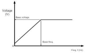
Fig 64 Voltage -frequency under constant v/f principle
The topology of a three-leg voltage source inverter is shown in Figure below. Because of the constraint that the input lines must never be shorted and the output current must always be continuous a voltage source inverter can assume only eight distinct topologies. These topologies are shown on Figure below. Six out of these eight topologies produce a nonzero output voltage and are known as non-zero switching states and the remaining two topologies produce zero output voltage and are known as zero switching states.
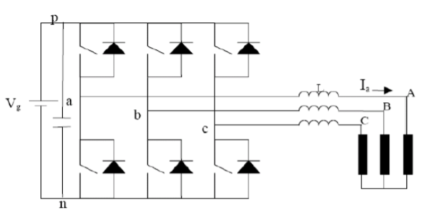
Fig 65 VSI
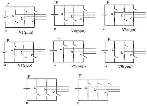
Fig 66 8-switching VSI
Space Vector Modulation (SVM) for three-leg VSI is based on the representation of the three phase quantities as vectors in a two-dimensional αβ plane. This is illustrated here for the sake of completeness. Considering topology 1 of Figure above, which is repeated in Fig.(a) below we see that the line voltages Vab, Vbc, and Vca are given by
Vab = Vg
Vbc = 0
Vca = -Vg
This can be represented in the αβ, plane as shown in Fig.(b), where voltages Vab, Vbc, and Vca are three-line voltage vectors displaced 120 in space. The effective voltage vector generated by this topology is represented as V1(pnn) in Fig.(b) below. Here the notation “pnn” refers to the three legs/phases a,b,c being either connected to the positive dc rail (p) or to the negative dc rail (n). Thus “pnn” corresponds to phase a being connected to the positive dc rail and phases b and c being connected to the negative dc rail.
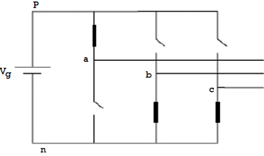
Fig 67(a) VI voltage source inverter
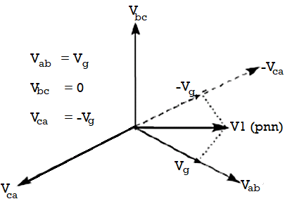
Fig 68 Representation in α plane
plane
Proceeding on similar lines the six non-zero voltage vectors (V1 - V6) can be shown to assume the positions shown in Fig. Below. The tips of these vectors form a regular hexagon (dotted line in Fig. Below). We define the area enclosed by two adjacent vectors, within the hexagon, as a sector. Thus, there are six sectors numbered 1 - 6 in Fig. Below.
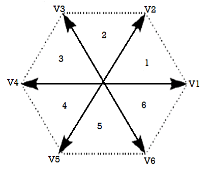
Fig 69 Non-zero voltage vectors in the αβ plane
Considering the last two topologies of Fig. Above which are repeated in Fig. (a) below for the sake of convenience we see that the output line voltages generated by this topology are given by
Vab = 0
Vbc = 0
Vca = 0
These are represented as vectors which have zero magnitude and hence are referred to as zero-switching state vectors or zero voltage vectors. They assume the position at origin in the αβ, plane as shown in Fig. (b) below. The vectors V1-V8 are called the switching state vectors (SSVs).
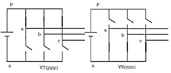
Fig 70(a) Zero output voltage
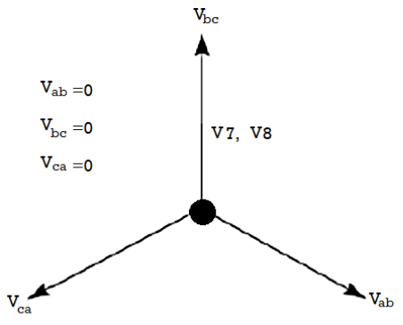
Fig 71(b) Representation of the zero voltage vectors in the αβ plane
Consider 3-phase inverter as shown below
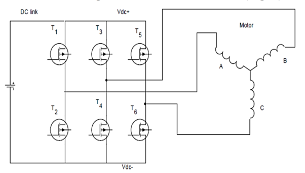
Fig 72 Inverter Bridge Configuration
The six-switch combination in the inverter has eight permissible switching states. Table below summaries these states along with the corresponding line to neutral voltage applied to the motor.
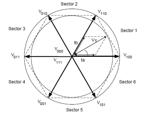
Fig 73 Space vector Diagram
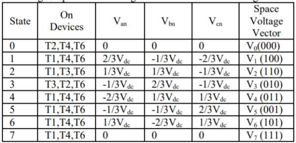
SVPWM seeks to average out the adjacent vectors for each sector. Using the appropriate PWM signals a vector is produced that transitions smoothly between sectors and thus provide sinusoidal line to line voltages to the motor. In order to generate the PWM signals that produce the rotating vector, formulae must be derived to determine the PWM time intervals for each sector. The reference vector is represented in a αβ-plane. This is a two-dimensional plane transformed from a three-dimensional plane containing the vectors of the three phases. The switches being ON or OFF are determined by the location of the reference vector on this αβ-plane.
The three-phase system is balanced when
Va0 +Vb0 + Vc0 =0
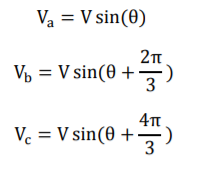


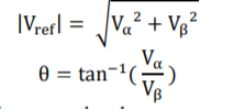


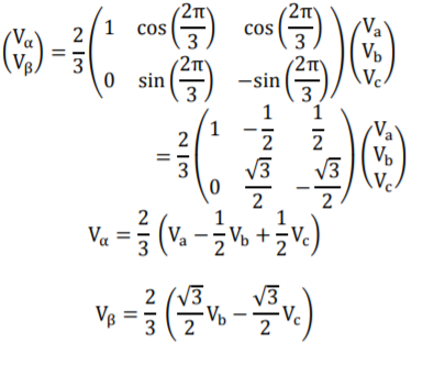
For each sector there are 7 switching states for each cycle. It always starts and ends with a zero vector. This also means that there is no extra switching state needed when changing the sector. The uneven numbers travel counter clockwise in each sector and the even sectors travel clockwise. Duty cycle for sector 1 for sector 1 it goes through these switching states: 000-100-110-111-110-100- 000, one round and then back again. This is during the time Tc and it has to be divided amongst the 7 switching states, three of them being zero vectors
Tc = T0/4 + T1/2 + T0/2 + T2/2 + T1/2 + T0/4
QAM for Wireless Communication
Another major development occurred in 1987 when Sundberg, Wong and Steele published a pair of papers. Considering QAM for voice transmission over Rayleigh fading channels, the first major paper considering QAM for mobile radio applications. In these papers, it was recognized that when a Gray code mapping scheme was used, some of the bits constituting a symbol had different error rates from other bits. Gray coding is a method of assigning bits to be transmitted to constellation points in an optimum manner. For the 16-level constellation two classes of bits occurred, for the 64-level three classes and so on. Efficient mapping schemes for pulse code modulated (PCM) speech coding was, discussed where the most significant bits (MSBs) were mapped onto the class with the highest integrity. A number of other schemes including variable threshold systems and weighted systems were also discussed. Simulation and theoretical results were compared and found to be in reasonable agreement. They used no carrier recovery, clock recovery or AGC, assuming these to be ideal, and came to the conclusion that channel coding and post-enhancement techniques would be required to achieve acceptable performance.
This work was continued, resulting in a publication in 1990 by Hanzo, Steele and Fortune, again considering QAM for mobile radio transmission, where again a theoretical argument was used to show that with a Gray encoded square constellation, the bits encoded onto a single symbol could be split into a number of subclasses, each subclass having a different average BER. The authors then showed that the difference in BER of these different subclasses could be reduced by constellation distortion at the cost of slightly increased total BER, but was best dealt with by using different error correction powers on the different 16- QAM subclasses. A 16 kbit/s sub-band speech coder was subjected to bit sensitivity analysis and the most sensitive bits identified were mapped onto the higher integrity 16-QAM subclasses, relegating the less sensitive speech bits to the lower integrity classes. Furthermore, different error correction coding powers were considered for each class of bits to optimise performance. Again, ideal clock and carrier recovery were used, although this time the problem of automatic gain control (AGC) was addressed. It was suggested that as bandwidth became increasingly congested in mobile radio, microcells would be introduced supplying the required high SNRs with the lack of bandwidth being an incentive to use QAM.
In the meantime, CNET were still continuing their study of QAM for point-to-point applications, and detailing an improved carrier recovery system using a novel combination of phase and frequency detectors which seemed promising. However, interest was now increasing in QAM for mobile radio usage and a paper was published in 1989 by J. Chuang of Bell Labs considering NLF-QAM for mobile radio and concluding that NLF offered slight improvements over raised cosine filtering when there was mild intersymbol interference (ISI).
A technique, known as the transparent tone in band method (TTIB) was proposed by McGeehan and Bateman from Bristol University, UK, which facilitated coherent detection of the square QAM scheme over fading channels and was shown to give good per-formance but at the cost of an increase in spectral occupancy. At an IEE colloquium on multilevel modulation techniques in March 1990 a number of papers were presented considering QAM for mobile radio and point-to-point applications. Matthews proposed the use of a pilot tone located in the centre of the frequency band for QAM transmissions over mobile channels. Huish discussed the use of QAM over fixed links, which was becoming increasingly widespread. Webb et al. Presented two papers describing the problems of square QAM constellations when used for mobile radio transmissions and introduced the star QAM constellation with its inherent robustness in fading channels.
Further QAM schemes for hostile fading channels characteristic of mobile telephony can be found in the following recent references. If Feher’s previously mentioned NLA concept cannot be applied, then power-inefficient class A or AB linear amplification has to be used, which might become an impediment in lightweight, low-consumption handsets. However, the power consumption of the low-efficiency class A amplifier is less critical than that of the digital speech and channel codecs. In many applications 16- QAM, transmitting 4 bits per symbol reduces the signalling rate by a factor of 4 and hence mitigates channel dispersion, thereby removing the need for an equaliser, while the higher SNR demand can be compensated by diversity reception.
A further important research trend is hallmarked by Cavers’ work targeted at pilot symbol assisted modulation (PSAM), where known pilot symbols are inserted in the information stream in order to allow the derivation of channel measurement information. The recovered received symbols are then used to linearly predict the channel’s attenuation and phase. A range of advanced QAM modems have also been proposed by Japanese researchers doing cutting-edge research in the field.
References:
1. Integrated Devices & Circuits by Millman & Halkias, TMH Publications.
2. Electronics Devices and Circuit Theory by R. Boylestad & L. Nashelsky, Pearson Publication
3. Electronic Communication System by G. Kennedy, TMH Publications.
4. Basic Electronics by Sanjeev Kumar & Vandana Sachdeva, Paragaon International Publication