Unit - 5
Digital Logic and basic circuit Design
A digital system understands positional number system where there are few symbols called digits and these symbols represents different values depending on their position in the number.
A value of the digit is determined by using
- The digit
- Its position
- The base of the number system
Decimal Number System
- It’s the system that we use in our daily life. It has a base 10 and uses 10 digits from 0 to 9.
- Here, the successive positions towards the left of the decimal point represent units, tens, hundreds, thousands and so on.
- Each and every position represents a specific power of the base (10). For example, the decimal number 4321 consists of the digit 1 in the unit’s position, 2 in the tens position, 3 in the hundreds position, and 4 in the thousands position, and its value can be written as
(1×1000) + (2×100) + (3×10) + (4×l)
(1×10³) + (2×10²) + (3×101) + (4×l00)
1000 + 200 + 30 + 1
1234
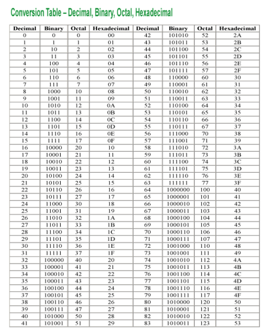
- As a computer programmer, we should understand the following number systems used in computers.
S.N. | Number System & Description |
1 | Binary Number System Base 2. Digits used: 0 and 1 |
2 | Octal Number System Base 8. Digits used: 0 to 7 |
3 | Hexa Decimal Number System Base 16. Digits used: 0 to 9, Letters used: A- F |
Binary Number System
- It uses two digits 0 and 1.
- It is also called as base 2 number system.
- Here, each position in any binary number represents a power of the base (2). Example: 23
- The last position represents a y power of the base (2). Example: 2y where y represents the last position.
Example
Binary Number: 101112
Calculating the Decimal Equivalent of binary number −
Step | Binary Number | Decimal Number |
Step 1 | 101012 | ((1 × 24) + (0 × 23) + (1 × 22) + (1 × 21) + (1 × 20))10 |
Step 2 | 101012 | (16 + 0 + 4 + 2 + 1)10 |
Step 3 | 101012 | 2310 |
Note: 101112 is normally written as 10111.
Octal Number System
- It consists of eight digits 0, 1,2,3,4,5,6,7.
- It is also named as base 8 number system.
- Here each position represents a power of the base (8). Example: 82
- The last position represents a y power of the base (8). Example: 8y where y represents the last position.
Example
Octal Number − 125758
Calculating Decimal Equivalent −
Step | Octal Number | Decimal Number |
Step 1 | 125758 | ((1 × 84) + (2 × 83) + (5 × 82) + (7 × 81) + (5 × 80))10 |
Step 2 | 125758 | (4096 + 1024 + 320 + 56 + 5)10 |
Step 3 | 125758 | 550010 |
Note: 125758 is normally written as 12575 in octal.
Hexadecimal Number System
- It uses 10 digits starting from 0,1,2,3,4,5,6,7,8,9 and 6 letters A, B, C, D, E, F.
- These letters represent numbers as A = 10, B = 11, C = 12, D = 13, E = 14, F = 15.
- It is also known as base 16 number system.
- Here each position represents a power of the base (16). Example 161.
- The last position represents a y power of the base (16). Example: 16y where y represents the last position.
Example −
Hexadecimal Number: 19FDA16
Calculating Decimal Equivalent −
Step | Hexadecimal Number | Decimal Number |
Step 1 | 19FDA16 | ((1 × 164) + (9 × 163) + (F × 162) + (D × 161) + (A × 160))10 |
Step 2 | 19FDA16 | ((1 × 164) + (9 × 163) + (15 × 162) + (13 × 161) + (10 × 160))10 |
Step 3 | 19FDA16 | (65536 + 36864 + 3840 + 208 + 10)10 |
Step 4 | 19FDA16 | 10645810 |
Note − 19FDA16 is normally written as 19FDA in hexa decimal.
Conversions:
There are many techniques which are used to convert numbers from one base to another. These are as follows −
- Decimal to any other Base System
- Any Base System to Decimal
- Any Base System to Non-Decimal
- Binary to Octal
- Octal to Binary
- Binary to Hexadecimal
- Hexadecimal to Binary
Decimal to Any Base System
It includes the following steps:
- Firstly, divide the decimal number which is to be converted by the value of its new base.
- Then, after getting the remainder from the above step make it the rightmost digit (least significant digit) i.e., LSD of new base number.
- Further divide the quotient by the new base.
- Then record the remainder from the above step as the next digit (towards the left) of the new base number.
- Repeat these steps and get remainders from right to left till the quotient becomes zero.
- The last remainder obtained will be the Most Significant Digit (MSD) of the new base number.
For example −
Decimal Number: 2710
Calculating Binary Equivalent –
Step | Operation | Result | Remainder |
Step 1 | 27 / 2 | 13 | 1 |
Step 2 | 13 / 2 | 6 | 1 |
Step 3 | 6 / 2 | 3 | 0 |
Step 4 | 3 / 2 | 1 | 1 |
Step 5 | 1 / 2 | 0 | 1 |
Hence, the remainders are arranged in the reverse order and we get:
Decimal Number − 2710 = Binary Number − 110112.
Any Base System to Decimal System
- Here, the column (positional) value of each digit (this depends on the position of the digit and the base of the number system) is multiplied with the obtained column values of the digits in the corresponding columns.
- The sum the products is then calculated which gives the total equivalent value in decimal.
For example:
Binary Number − 111102
Calculating Decimal Equivalent –
Step | Binary Number | Decimal Number |
Step 1 | 111102 | ((1 × 24) + (1 × 23) + (1 × 22) + (1 × 21) + (0 × 20))10 |
Step 2 | 111102 | (16 + 8 + 4 + 2 + 0)10 |
Step 3 | 111102 | 3010 |
Binary Number − 111102 = Decimal Number − 3010
Any Base System to Non-Decimal System
- The original number is converted to its equivalent decimal number (base 10).
- Then the decimal number so obtained is further converted to the new base number.
Example
Octal Number − 268
Calculating its Binary Equivalent −
Step 1 – Converting octal to Decimal
Step | Octal Number | Decimal Number |
Step 1 | 268 | ((2 × 81) + (6 × 80))10 |
Step 2 | 268 | (16 + 6 )10 |
Step 3 | 268 | 2210 |
Octal Number − 268 = Decimal Number − 2210
Step 2 − Converting Decimal to Binary
Step | Operation | Result | Remainder |
Step 1 | 22 / 2 | 11 | 0 |
Step 2 | 11 / 2 | 5 | 1 |
Step 3 | 5 / 2 | 2 | 1 |
Step 4 | 2 / 2 | 1 | 0 |
Step 5 | 1 / 2 | 0 | 1 |
Decimal Number − 2210 = Binary Number − 101102
Octal Number − 268 = Binary Number − 101102
Binary to Octal
- Dividing the binary digits into groups of three starting from right to left.
- Converting each group of three binary digits into one octal digit.
For example:
Binary Number − 101012
Its Octal Equivalent −
Step | Binary Number | Octal Number |
Step 1 | 101012 | 010 101 |
Step 2 | 101012 | 28 58 |
Step 3 | 101012 | 258 |
Binary Number − 101012 = Octal Number − 258
Octal to Binary
- Converting each octal digit to a 3-digit binary number and they can be treated as decimal number for this conversion.
- Then combining all the resulting binary groups into a single binary number.
For example:
Octal Number − 258
Its Binary Equivalent –
Step | Octal Number | Binary Number |
Step 1 | 258 | 210 510 |
Step 2 | 258 | 0102 1012 |
Step 3 | 258 | 0101012 |
Octal Number − 258 = Binary Number − 101012
Binary to Hexadecimal
- Dividing the binary digits into groups of four (starting from right to left).
- Then converting each group of four binary digits into one hexadecimal number.
For example:
Binary Number − 101012
Its hexadecimal Equivalent –
Step | Binary Number | Hexadecimal Number |
Step 1 | 101012 | 0001 0101 |
Step 2 | 101012 | 110 510 |
Step 3 | 101012 | 1516 |
Binary Number − 101012 = Hexadecimal Number − 1516
Hexadecimal to Binary
- Converting each hexadecimal digit to a 4-digit binary number and they can be treated as decimal number.
- Combining all the resulting binary groups into a single binary number.
For example:
Hexadecimal Number − 1516
Its Binary Equivalent −
Step | Hexadecimal Number | Binary Number |
Step 1 | 1516 | 110 510 |
Step 2 | 1516 | 00012 01012 |
Step 3 | 1516 | 000101012 |
Hexadecimal Number − 1516 = Binary Number − 101012
Key takeaway
Binary Addition
- It is a basis for binary subtraction, multiplication, division.
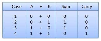
- There are four rules which are as follows:
Rules of Binary addition
In fourth step, a sum (1 + 1 = 10) i.e. 0 is written in the given column and a carry of 1 over to the next column is done.
For Example −

Binary addition
Binary Subtraction
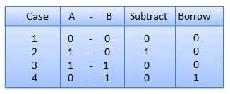
Subtraction and Borrow, these are the two words that will be used very frequently for binary subtraction. There rules of binary subtraction are:
Rules of Binary Subtraction
For Example

Fig. Binary subtraction
AND gate
It is a digital circuit that consists of two or more inputs and a single output which is the logical AND of all those inputs. It is represented with the symbol ‘.’.
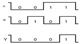
The following is the truth table of 2-input AND gate.
A | B | Y = A.B |
0 | 0 | 0 |
0 | 1 | 0 |
1 | 0 | 0 |
1 | 1 | 1 |
Here A, B are the inputs and Y is the output of two input AND gate.
If both inputs are ‘1’, then only the output, Y is ‘1’. For remaining combinations of inputs, the output, Y is ‘0’.
The figure below shows the symbol of an AND gate, which is having two inputs A, B and one output, Y.

Fig.: AND gate
Timing Diagram:
OR gate
It is a digital circuit which has two or more inputs and a single output which is the logical OR of all those inputs. It is represented with the symbol ‘+’.
The truth table of 2-input OR gate is:
A | B | Y = A + B |
0 | 0 | 0 |
0 | 1 | 1 |
1 | 0 | 1 |
1 | 1 | 1 |
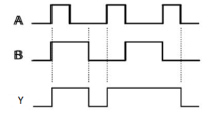
Here A, B are the inputs and Y is the output of two input OR gate.
When both inputs are ‘0’, then only the output, Y is ‘0’. For remaining combinations of inputs, the output, Y is ‘1’.
The figure below shows the symbol of an OR gate, which is having two inputs A, B and one output, Y.

Fig: OR gate
Timing Diagram:
NOT gate
It is a digital circuit that has one input and one output. Here the output is the logical inversion of input. Hence, it is also called as an inverter.
The truth table of NOT gate is:
A | Y = A’ |
0 | 1 |
1 | 0 |
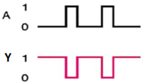
Here A and Y are the corresponding input and output of NOT gate. When A is ‘0’, then, Y is ‘1’. Similarly, when, A is ‘1’, then, Y is ‘0’.
The figure below shows the symbol of NOT gate, which has one input, A and one output, Y.

Fig: NOT gate
Timing Diagram:
Universal gates
- NAND & NOR gates are known as universal gates.
- We can implement any Boolean function by using NAND gates and NOR gates alone.
NAND gate
It is a digital circuit which has two or more inputs and single output and it is the inversion of logical AND gate.
The truth table of 2-input NAND gate is:
A | B | Y = (A.B)’ |
0 | 0 | 1 |
0 | 1 | 1 |
1 | 0 | 1 |
1 | 1 | 0 |
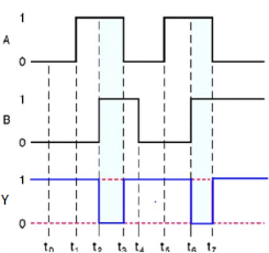
Here A, B are the inputs and Y is the output of two input NAND gate. When both inputs are ‘1’, then the output, Y is ‘0’. If at least one of the input is zero, then the output, Y is ‘1’. This is just the inverse of AND operation.
The image shows the symbol of NAND gate:

Fig: NAND gate
NAND gate works same as AND gate followed by an inverter.
Timing Diagram:
NOR gate
It is a digital circuit that has two or more inputs and a single output which is the inversion of logical OR of all inputs.
The truth table of 2-input NOR gate is:
A | B | Y = (A+B)’ |
0 | 0 | 1 |
0 | 1 | 0 |
1 | 0 | 0 |
1 | 1 | 0 |
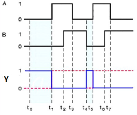
Here A and B are the two inputs and Y is the output. If both inputs are ‘0’, then the output is ‘1’. If any one of the input is ‘1’, then the output is ‘0’. This is exactly opposite to two input OR gate operation.
The symbol of NOR gate is:

Fig: NOR gate
NOR gate works exactly same as that of OR gate followed by an inverter.
Timing Diagram:
Special Gates
Ex-OR gate
It stands for Exclusive-OR gate. Its function varies when the inputs have even number of ones.
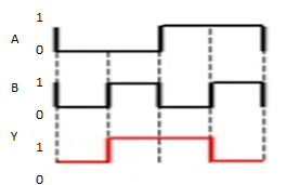
The truth table of 2-input Ex-OR gate is:
A | B | Y = A⊕B |
0 | 0 | 0 |
0 | 1 | 1 |
1 | 0 | 1 |
1 | 1 | 0 |
Here A, B are the inputs and Y is the output of two input Ex-OR gate. The output (Y) is zero instead of one when both the inputs are one.
Therefore, the output of Ex-OR gate is ‘1’, when only one of the two inputs is ‘1’. And it is zero, when both inputs are same.
The symbol of Ex-OR gate is as follows:

Fig: XOR gate
It is similar to that of OR gate with an exception for few combination(s) of inputs. Hence, the output is also known as an odd function.
Timing Diagram:
Ex-NOR gate
It stands for Exclusive-NOR gate. Its function is same as that of NOR gate except when the inputs having even number of ones.
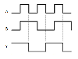
The truth table of 2-input Ex-NOR gate is:
A | B | Y = A⊙B |
0 | 0 | 1 |
0 | 1 | 0 |
1 | 0 | 0 |
1 | 1 | 1 |
Here A, B are the inputs and Y is the output. It is same as Ex-NOR gate with the only modification in the fourth row. The output is 1 instead of 0, when both the inputs are one.
Hence the output of Ex-NOR gate is ‘1’, when both inputs are same and 0, when both the inputs are different.
The symbol of Ex-NOR gate is:

Fig: XNOR gate
It is similar to NOR gate except for few combination(s) of inputs. Here the output is ‘1’, when even number of 1 is present at the inputs. Hence is also called as an even function.
Timing Diagram:
The three basic laws of Boolean Algebra are:
- Commutative law
- Associative law
- Distributive law
Commutative Law
- The logical operation carried between two Boolean variables when gives the same result irrespective of the order the two variables, then that operation is said to be Commutative. The logical OR & logical AND operations between x & y are shown below
x + y = y + x
x.y = y.x
- The symbol ‘+’ and ‘.’ indicates logical OR operation and logical AND operation.
- Commutative law holds good for logical OR & logical AND operations.
Associative Law
- If a logical OR operation of any two Boolean variables is performed first and then the same operation is performed with the remaining variable providing the same result, then that operation is said to be Associative. The logical OR & logical AND operations of x, y & z are:
x + (y + z) = (x + y) + z
x.(y.z) = (x.y).z
- Associative law holds good for logical OR & logical AND operations.
Distributive Law
- If a logical OR operation of any two Boolean variables is performed first and then AND operation is performed with the remaining variable, then that logical operation is said to be Distributive. The distribution of logical OR & logical AND operations between variables x, y & z are:
x.(y + z) = x.y + x.z
x + (y.z) = (x + y).(x + z)
- Distributive law holds good for logical OR and logical AND operations.
- These are the Basic laws of Boolean algebra and we can verify them by substituting the Boolean variables with ‘0’ or ‘1’.
Transistor raises the strength of a weak signal and hence acts an amplifier. The transistor amplifier circuit is shown in the figure below.
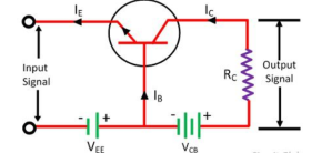
Figure. Transistor as an Amplifier
The transistor has three terminals namely emitter, base and collector. The emitter and base of the transistor are connected in forward biased and the collector base region is in reverse bias. The forward bias means the P-region of the transistor is connected to the positive terminal of the supply and the negative region is connected to the N-terminal and in reverse bias just opposite of it has occurred.
Vee is applied to the input circuit along with the input signal to achieve the amplification. The DC voltage VEE keeps the emitter-base junction under the forward biased condition regardless of the polarity of the input signal and is known as bias voltage.
When a weak signal is applied to the input, a small change in signal voltage causes a change in emitter current this change is almost the same in collector current because of the transmitter action.
In the collector circuit, a load resistor RC of high value is connected. When collector current flows through such a high resistance, it produces a large voltage drop across it. Thus, a weak signal (0.1V) applied to the input circuit appears in the amplified form (10V) in the collector circuit.
Input Resistance
When the input circuit is forward biased, the input resistance will be low. The input resistance is the opposition offered by the base-emitter junction to the signal flow.
Hence, it is the ratio of small change in base-emitter voltage (ΔVBE) to the resulting change in base current (ΔIB) at constant collector-emitter voltage.
Input resistance, Ri=ΔVBE/ΔIb
Where Ri = input resistance, VBE = base-emitter voltage, and IB = base current.
Output Resistance
The output resistance of a transistor amplifier is very high. The collector current changes very slightly with the change in collector-emitter voltage.
The ratio of change in collector-emitter voltage (ΔVCE) to the resulting change in collector current (ΔIC) at constant base current.
Output resistance = Ro=ΔVCE/ΔIC
Where Ro = Output resistance, VCE = Collector-emitter voltage, and IC = Collector-emitter voltage.
Current gain
It is the ratio of change in collector current (ΔIC) to the change in base current (ΔIB).
Current gain, β=ΔIC/ ΔIB
Voltage Gain
It is the ratio of change in output voltage (ΔVCE) to the change in input voltage (ΔVBE).
Voltage gain, AV=ΔVCE/ΔVBE

Power Gain
It is the ratio of output signal power to the input signal power.
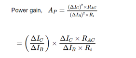
= current gain x voltage gain
Circuit configurations that may be used to convert the information voltage signal at the transmitter into a modulation current suitable for an LED source. LED drive circuits are typically designed to control the current running through a string of LEDs independent of the voltage drop across the LED string.
Digital transmission:
- The operation of the LED for binary digital transmission requires the switching on and off of a current in the range of several tens to several hundreds of milli-amperes.
- This must be performed at high speed in response to logic voltage levels at the driving circuit input. A common method of achieving this current switching operation for an LED is shown in Figure
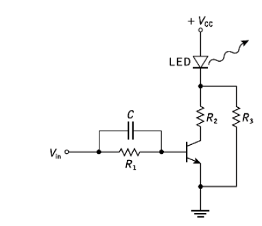
- The circuit illustrated uses a bipolar transistor switch operated in the common emitter mode.
- This single-stage circuit provides current gain as well as giving only a small voltage drop across the switch when the transmitter is in saturation.
- The maximum current flow through the LED is limited by the resistor R2 while independent bias to the device may be provided by the incorporation of resistor R3.
- The switching speed of the common emitter configuration is limited by space charge and diffusion capacitance; thus bandwidth is traded for current gain.
- This may be compensated by overdriving (pre-emphasizing) the base current during the switch-on period. In the circuit shown in Figure pre-emphasis is accomplished by use of the speed-up capacitor C.
Low-impedance drive circuit:
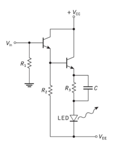
- Increased switching speed may be obtained from an LED without a pulse shaping or speed-up element by use of a low-impedance driving circuit, whereby charging of the space charge and diffusion capacitance occurs as rapidly as possible.
- This may be achieved with the emitter follower drive circuit shown in Figure.
- The use of this configuration with a compensating matching network (R3C) provides fast direct modulation of LEDs with relatively low drive power.
- A circuit, with optimum values for the matching network, is capable of giving optical rise times of 2.5 ns for LEDs with capacitance of 180 pF, thus allowing 100 Mbit s−1 operations.
The most commonly used wireless technology is the IR communication. This technology is employed in remotes mostly of TV and AC. The receiver senses the modulated IR pulse and converts it into electrical signal. The receiver is TSOP1738 which is generally used. The IR LED are used as transmitters. Below we will study in detail with the circuit diagram and working.
As we know that the IR light is not visible through naked eyes as they are beyond the visible range. Although they are above the visible light range but has few qualities like polarization, reflection which helps in wireless technology.
IR Transmitter
Here Astable multivibrator is used to produce oscillating frequency. The multivibrator is made out of IC 555 timer. The circuit generates output frequency of around 38kHz which is accomplished by circuit elements R1=1k , R2=20k
 and capacitor of 1nF.
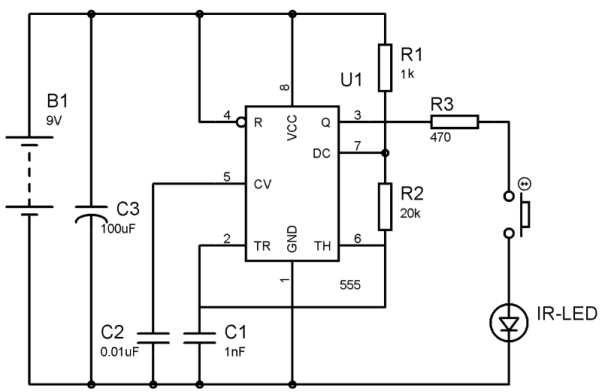
Fig IR Transmitter
The output is taken from pin 3 which is connected to 470 resistor and a push button switch. The circuit produces modulated IR signal of 38kHz approx. When ever the push button is pressed.
IR Receiver
Here TSOP1738 output is connected to the LED. A transistor Q1 which is PNP transistor is used which turns off when output from TSOP is high. Whenever IR is detected the output of it goes low and this turns ON the LED. When output from TSOP is high the transistor acts as open circuit and LED is turned OFF. The 10k resistor is used for providing proper biasing to the transistor. The 470 resistor is used to limit the current at LED.
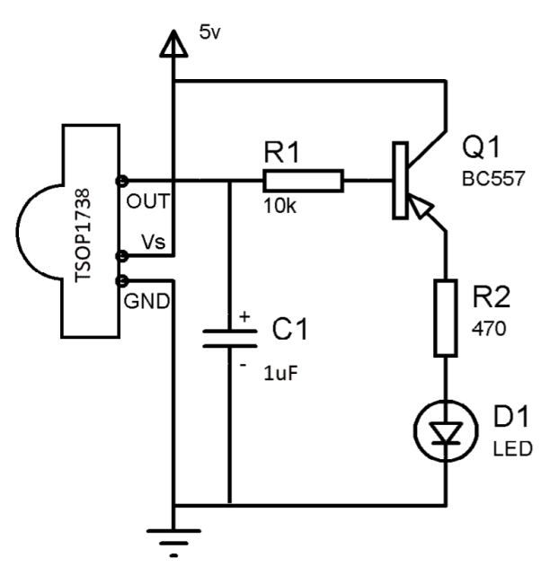
Fig IR Receiver
It is a device which has its resistivity is a function of the incident electromagnetic radiation. These devises are light sensitive. They fall under category of photoconductors, photoconductive cells. The high resistance semiconductor is used for making LDR. The symbol for LDR is shown below.
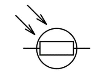
Fig LDR
The basic principle of photoresistor is photoconductivity. This is an optical phenomenon where conductivity of material is increased when light is absorbed by the material. The photons when falls on the device valance band electrons are excited and jumps to the conduction band. These electrons have higher energy which is more than the band gap of the material. This helps them to jump from the valance band. Hence large number of charge carriers are generated when light strikes the material and current starts to flow.
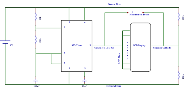
Fig LCD Driver Circuit
This shows that the resistance of the device decreases as the current flow increases. The LDR have very low resistance when light falls and the resistance value increases when kept in dark. If a constant voltage is applied to it and the intensity of light is increased the current starts increasing.
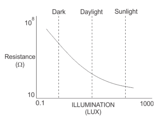
Fig Resistance and Illuminance Curve
There are two types of LDR’s. Based on the material used for construction there are two types of photoresistors. Intrinsic LDR are made of pure semiconductor such as Si and Ge. Here the electrons are excited from VB to CB when light falls on them and carriers are increased. Extrinsic LDR are made by adding impurity to the semiconductor material. Due to impurity the new energy bands are created above the valance band. Due to which the bandgap is reduced and less energy is required to excite them. For long wavelength we use these LDR.
A circuit which can drive a relay is called relay driver circuit. This circuit acts as switch which open and close as per the requirement of the circuit. The relay driver can be of following types
DC Relay Driver Circuit
In these circuits the relay behaves as an inductor. In many devices when there is voltage spike the current in the coil is suddenly interrupted and a large voltage is produced across it producing large amount of current. This huge amount of current can damage the near by devices. To overcome this, we use diode with the DC relay circuit.
The DC relay driver circuit has mainly three components DC relay, Zener Diode and DC voltage source.
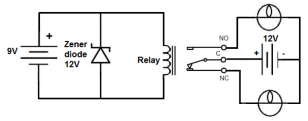
Fig DC Relay Circuit
The Zener diode is connected in reverse bias in the circuit. Supply of 9V is used and the Zener diode is connected in parallel with the relay. All the excess power is shunt to ground once a certain threshold is reached.
AC Relay Driver Circuit
This relay runs on AC power. For instance, if we need 110V from an AC power we require 110V ac supply. A capacitor and resistor in series are connected which acts as transient voltage suppressor. Relay driver serves as the first half of the relay driver. When there is sufficient power in relay it will turn on and will power to load to which it is connected.
Generic Relay Circuit
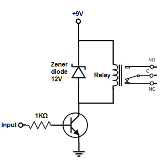
Fig Relay Driver
The circuit which can be driven by both ac and dc input voltage are called generic relay circuits. A transistor is used to drive the relay which uses less power. As transistor acts as an amplifier the base of the transistor should be supplied with enough current such that proper amount of current flows from emitter to the collector. Now the transistor starts conducting.
With no voltage or input current applied to the transistor's base lead, the transistor's emitter-to-collector channel is open, hence blocking current flow through the relay's coil. However, if sufficient voltage and input current are applied to the base lead, the transistor's emitter-to-collector channel will close, allowing current to flow through the relay's coil.
Square wave Oscillation using Astable Multivibrator
The astable multivibrator shown in the figure below [Ref.1] can be used to generate square wave oscillations. The diode is connected across RB and the diode and capacitor are charged through RA to a voltage of 2/3 of VCC. The capacitor discharges through RB and Q1. The discharging of capacitor when reaches 1/3VCC the discharging stops.

Fig. Astable multivibrator as square wave oscillator
Square wave Oscillation using Monostable Multivibrator
It also called one shot, operates by charging a timing capacitor with a current set by external resistance. When the one shot is triggered, the charging network cycles only once during the timing interval. The total timing interval includes the recovery time needed for the capacitor to charge up to the threshold level.
When Vcc high is applied to the trigger input, the trigger comparator output is low, the flip flop output is high, the transistor is on, the timing capacitor is discharged to ground potential. The output of the 555 circuit is low.
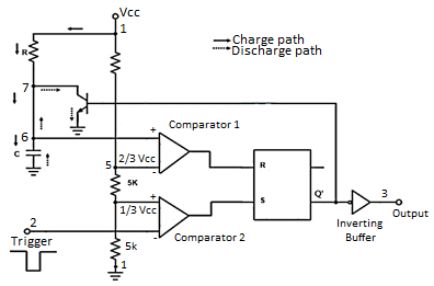
Fig. Monostable multivibrator
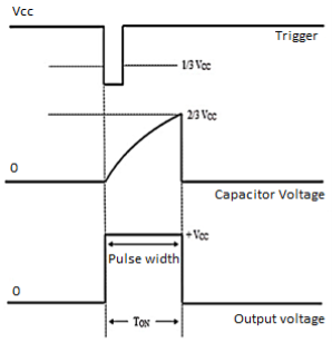
Fig. Output waveform
When negative voltage is applied to the trigger input, output of trigger comparator goes high. When trigger pulse drops below 1/3 Vcc output of flip flop goes low, output of 555 circuit goes high and the transistor turns off
Fixed Frequency generator
This means there will be no stable level at the output. So, the output will be swinging between high and low. This character of unstable output is used as a clock or square wave output for many applications.
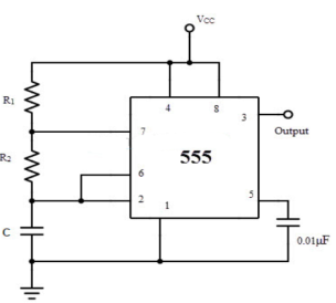
Fig. Astable Multivibrator
It is self-triggered multivibrator as pin 2 and 6 are connected. The supply is given through pin 8 and the output is obtained through pin 3. The timer will be reset if a low signal is given to pin 4. The capacitor is connected across pin 5 so that the external noise or any dc level are filtered. The resistor pair R1 and R2 form a circuit for determining the width of the output pulse.
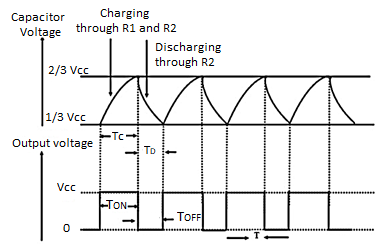
Fig. Capacitor and Output voltage waveform
During charging the capacitor charges through R1 and R2 and voltage across capacitor rises exponentially and during discharging the capacitor discharges through R2 and voltage falls exponentially. The output is obtained across pin 3.
The time for which capacitor charges from 1/3VCC to 2/3VCC is equal to the time the output is high which is given by
tc= 0.69(R1+R2) C
The discharging time from 2/3Vcc to 1/3VCC is given as
td= 0.69 R2C
The total period of output waveform is given by
T = tc+ td = 0.69(R1+2R2) C
The frequency of oscillations is given by
f0 =  =
= 
The duty cycle is defined as the ratio of the charging time of capacitor at which the output is high to the total time period.
%duty cycle =  x 100
x 100
Key takeaways
It also called one shot, operates by charging a timing capacitor with a current set by external resistance.
References:
1. Integrated Devices & Circuits by Millman & Halkias, TMH Publications.
2. Electronics Devices and Circuit Theory by R. Boylestad & L. Nashelsky, Pearson Publication
3. Electronic Communication System by G. Kennedy, TMH Publications.
4. Basic Electronics by Sanjeev Kumar & Vandana Sachdeva, Paragaon International Publication