Unit - 4
Sequential Circuits Elements
- A Sequential circuit consists of inputs variable (X), logic gates and output variable (Z).
- Combinational circuit generates an output on the basis of input variable only but Sequential circuit produces an output based on current input and previous output variables.
- This means that it includes memory elements which are capable of storing binary information.
- This binary information is nothing but the state of the sequential circuit at any given time. A latch capable of storing one bit information.

Fig. Combinational circuit
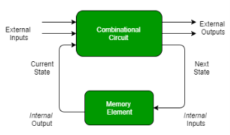
Fig. Sequential circuit
There are two types of input to the combinational logic in fig 2:
- External inputs which are not controlled by the circuit.
- Internal inputs which are function of previous output states.
Secondary inputs are state variables that are produced by the storage elements whereas secondary outputs are excitations for those storage elements.
Types of Sequential Circuits –
There are two types of sequential circuit:
Asynchronous sequential circuit –
- They do not use a clock signal but instead uses the pulses as inputs.
- These circuits are faster because there is clock pulse and can change their state immediately when there is a change in the input signal.
- It is used when speed of operation is important and is independent of internal clock pulse.

Fig. Asynchronous Sequential circuit
But they are more difficult to design and their output is also uncertain.
Synchronous sequential circuit –
- These circuit uses clock signal and level inputs.
- The output pulse is received in the same duration as the clock pulse for the clocked sequential circuits.
- They wait for the next clock pulse to arrive to perform the next operation, these circuits are bit slower as compared to asynchronous circuits.
- Level output changes state at the start of an input pulse and remains in that state until the next input or clock pulse arrives.
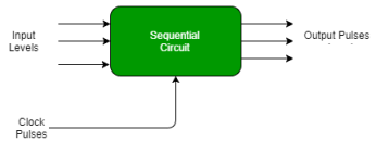
Fig. Synchronous Sequential circuit
- It is used in synchronous counters, flip flops, and in MOORE-MEALY machines.
- It is also used to design Counters, Registers, RAM, etc
Key takeaway
Asynchronous sequential circuit –
- They do not use a clock signal but instead uses the pulses as inputs.
- These circuits are faster because there is clock pulse and can change their state immediately when there is a change in the input signal.
Synchronous sequential circuit –
- These circuit uses clock signal and level inputs.
- The output pulse is received in the same duration as the clock pulse for the clocked sequential circuits.
Latches
- In digital electronics, a Latch is one kind of a logic circuit, and it is also known as a bistable-multivibrator. Because it has two stable states namely active high as well as active low.
- It works like a storage device by holding the data through a feedback lane.
- It stores 1-bit of data as long as the apparatus is activated. Once enable is declared then instantly latch can change the stored data. It constantly trials the inputs once enable signal is activated.
- The working of these circuits can be done in 2-states based on the enable signal being high or else low. When the latch circuit is the in an active high state, then both the i/ps are low. Similarly, when the latch circuit is then an active low state, then both the i/ps are high.
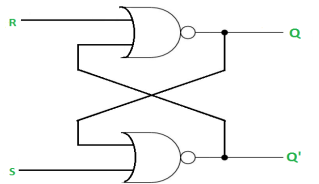
SR Latch is a circuit which has:
(i) 2 cross-coupled NOR gate or NAND gate.
(ii) 2 input S for SET and R for RESET.
(iii) 2 output Q and Q’.
Q | Q’ | STATE |
1 | 0 | Set |
0 | 1 | Reset |
Under normal conditions, both the input remains 0.
RS Latch with NAND gates:
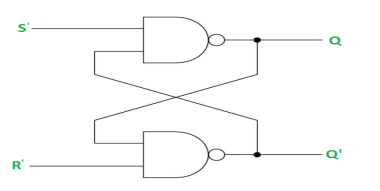
Case-1: When S’=R’=1 or S=R=0 then
If Q = 1, Q = R’ = 1.
If Q = 0, Q = 0 and R’ = 1 respectively.
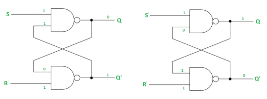
Case-2: S’=0, R’=1 (S=1, R=0)
As S’=0, Q = 1(SET state).
In 2nd NAND gate, as Q = R’ = 1, Q’=0.
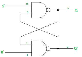
Case-3: S’= 1, R’= 0 (S=0, R=1)
As R’=0, Q’ = 1.
In 1st NAND gate, as Q =S’ = 1, Q=0 (RESET state).
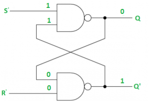
Case-4: S’= R’= 0 (S=R=1)
When S=R=1, both Q = Q’ = 1 which is not allowed.
So, this input condition is prohibited.
The SR Latch using NOR gate is:
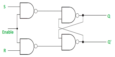
Gated SR Latch –
It is a latch which enable input that works when enable = 1 and retain the previous state when enable = 0.
Gated D Latch –
It is similar to SR latch with little modifications. Here, the inputs are complements of one another. The design of D latch with Enable signal is given below:
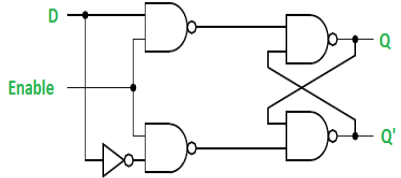
The truth table is shown below:
ENABLE | D | Q(N) | Q(N+1) | STATE |
1 | 0 | x | 0 | RESET |
1 | 1 | x | 1 | SET |
0 | x | x | Q(n) | No Change |
As the output is same as input, it is also known as Transparent Latch.
The characteristic equation for D latch with enables input is given as:
Q(n+1) = EN.D + EN'.Q(n)
S-R Flip Flop:
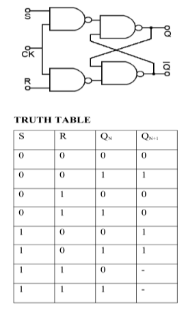
J-K Flip Flop:
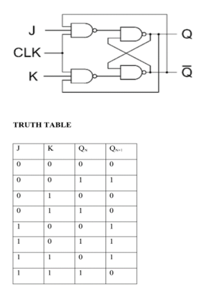
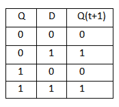
D Flip Flop:
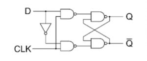
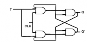
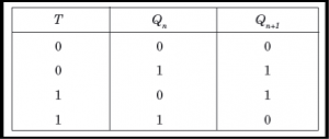
T Flip Flop:
- Some flip-flops have asynchronous inputs that are used to force the flip-flop to a particular state independently of the clock
- The input that sets the flip-flop to 1 is called preset or direct set. The input that clears the flip-flop to 0 is called clear or direct reset.
- When power is turned on in a digital system, the state of the flip-flops is unknown. The direct inputs are useful for bringing all flip-flops in the system to a known starting state prior to the clocked operation.
- The knowledge of the type of flip-flops and a list of the Boolean expressions of the combinational circuit provide the information needed to draw the logic diagram of the sequential circuit. The part of the combinational circuit that gene rates external outputs is described algebraically by a set of Boolean functions called output equations. The part of the circuit that generates the inputs to flip-flops is described algebraically by a set of Boolean functions called flip-flop input equations (or excitation equations).
- The information available in a state table can be represented graphically in the form of a state diagram. In this type of diagram, a state is represented by a circle and the (clock-triggered) transitions between states are indicated by directed lines connecting the circles.
- The time sequence of inputs, outputs, and flip-flop states can be enumerated in a state table (transition table). The table has four parts present state, next state, inputs and outputs.
- In general, a sequential circuit with 'm' flip-flops and 'n' inputs needs 2m+n rows in the state table.
Positive Edge Triggered D Flip-flop
- A circuit diagram of a Positive edge triggered D Flip-flop is shown as below. It has an additional reset input connected to the three NAND gates.
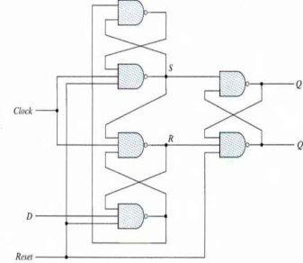
Fig: Circuit Diagram
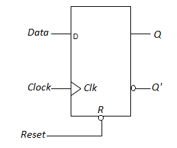
Fig: Symbol
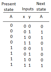
Fig: State Table
- When the reset input is 0 it forces output Q' to Stay at 1 which clears output Q to 0 thus resetting the flip-flop.
- Two other connections from the reset input ensure that the S input of the third SR latch stays at logic 1 while the reset input is at 0 regardless of the values of D and Clk.
- Function table suggests that:
- When R = 0, the output is set to 0 (independent of D and Clock).
- The clock at Clock is shown with an upward arrow to indicate that the flip-flop triggers on the positive edge of the clock.
- The value in D is transferred to Q with every positive-edge clock signal provided that R = 1.
Analysis with D Flip-Flops
- The input equation of a D Flip-flop is given by DA = A ⊕ x ⊕ y. DA means a D Flip-flop with output A.
- The x and y variables are the inputs to the circuit. No output equations are given, which implies that the output comes from the output of the flip-flop.
- The state table has one column for the present state of flip-flop 'A' two columns for the two inputs, and one column for the next state of A.
- The next-state values are obtained from the state equation A (t + 1) = A ⊕ x ⊕ y.
- The expression specifies an odd function and is equal to 1 when only one variable is 1 or when all three variables are 1.
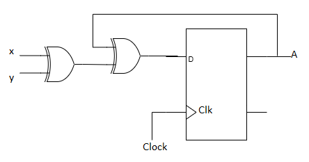
Fig: Circuit Diagram
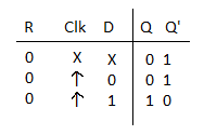
Fig: State Table
Analysis with JK Flip-Flops
- The circuit can be specified by the flip-flop input equations:
- JA = B; KA = Bx'
- JB = x'; KB = A'x + Ax' = A ⊕ x
- The next state of each flip-flop is evaluated from the corresponding J and K inputs and the characteristic table of the JK flip-flop listed as:
- When J = 1 and K = 0 the next state is 1
- When J = 0 and K = 1 the next state is 0
- When J = 0 and K = 0 there is no change of state and the next-state value is the same as that of the present state.
- When J = K = 1, the next-state bit is the complement of the present-state bit.
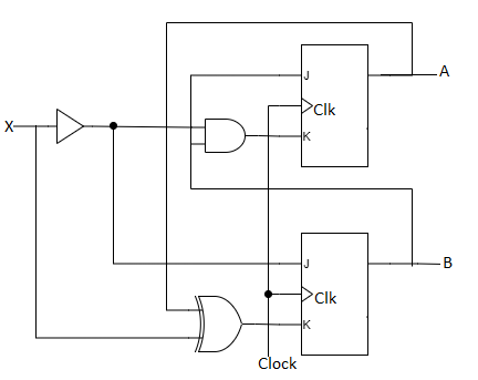
Fig: Circuit Diagram
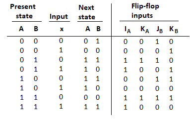
Fig: State Table
- The characteristic equations for the flip-flops are
- A (t + 1) = JA' + K'A
- B (t + 1) = JB' + K'B
- This gives us the state equation of A by substituting the values of JA, KA
A (t + 1) = BA' + (Bx')'A = A'B + AB' + Ax
- The state equation provides the bit values for the column headed "Next State" for A in the state table. Similarly, the state equation for flip-flop B can be derived from the characteristic equation by substituting the values of JB and KB.:
- B (t + 1) = x'B' + (A ⊕ x)'B = B'x' + ABx + A'Bx'
Analysis with T Flip-Flops
- The circuit can be specified by the characteristic equations:
- Q(t+1) = T ⊕ Q = T'Q + TQ'
- The sequential circuit has two flip-flops A and B, one input x, and one output y and can be described algebraically by two input equations and an output equation.
- TA = Bx
- TB = x
- y = AB
- The state table for the circuit is listed below. The values for y are obtained from the output equation. The values for the next state can be derived from the state equations by substituting TA and TB in the characteristic equations yielding:
- A (t + 1) = (Bx)' A + (Bx)A' = AB' + Ax' + A'Bx
- B (t + 1) = x ⊕ B
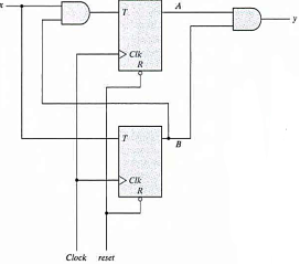
Fig: Circuit Diagram
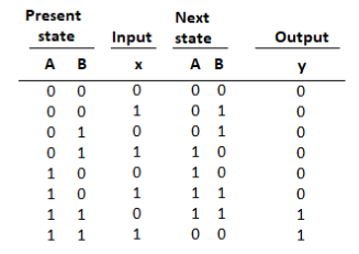
Fig: State Table
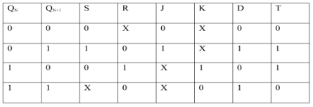
EXCITATION TABLE:
Race Around Condition in JK Flip-flop –
- For J-K flip-flop, if J=K=1, and if clk=1 for a long period of time, then output Q will toggle as long as CLK remains high which makes the output unstable or uncertain.
- This problem is known as race around condition in J-K flip-flop.
- This problem can be avoided by ensuring that the clock input is at logic “1” only for a very short time.
- Hence the concept of Master Slave JK flip flop was introduced.
Master Slave JK flip flop –
It is basically a combination of two JK flip-flops connected together in series.
The first is the “master” and the other is a “slave”.
The output from the master is connected to the two inputs of the slave whose output is fed back to inputs of the master.
In addition to these two flip-flops, the circuit comprises of an inverter.
The inverter is connected to clock pulse in such a way that an inverted clock pulse is given to the slave flip-flop.
In other words, if CP=0 for a master flip-flop, then CP=1 for a slave flip-flop and vice versa.
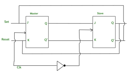
Fig. Master Slave Flip flop
Working of a master slave flip flop –
- When the clock pulse goes high, the slave is isolated; J and K inputs can affect the state of the system. The slave flip-flop is isolated when the CP goes low. When the CP goes back to 0, information is transmitted from the master flip-flop to the slave flip-flop and output is obtained.
- The master flip flop is positive level triggered and the slave flip flop is negative level triggered, hence the master responds prior to the slave.
- If J=0 and K=1, Q’ = 1 then the master goes to the K input of the slave and the clock forces the slave to reset therefore the slave copies the master.
- If J=1 and K=0, Q = 1 then the master goes to the J input of the slave and the Negative transition of the clock sets the slave and thus copy the master.
- If J=1 and K=1, the master toggles on the positive transition and the slave toggles on the negative transition of the clock.
- If J=0 and K=0, the flip flop becomes disabled and Q remains unchanged.
Timing Diagram of a Master flip flop –
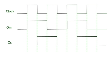
- When the CP = 1 then the output of master is high and remains high till CP = 0 because the state is stored.
- Now the output of master becomes low when the clock CP = 1 and remains low until the clock becomes high again.
- Thus, toggling takes place for a clock cycle.
- When the CP = 1 then the master is operational but not the slave.
- When the clock is low, the slave becomes operational and remains high until the clock again becomes low.
- Toggling takes place during the whole process since the output changes once in a cycle.
- This makes the Master-Slave J-K flip flop a Synchronous device which passes data with the clock signal.
Conversion for flip flops:
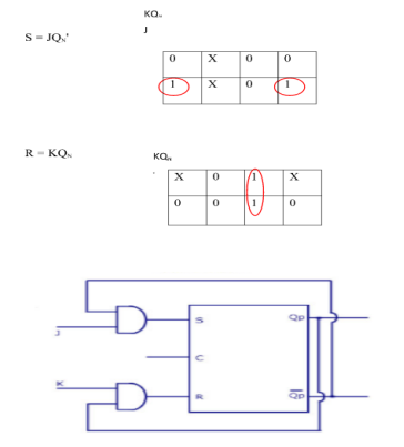
i) SR To JK FlipFlop
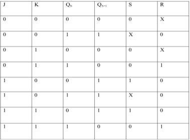
Excitation Functions:
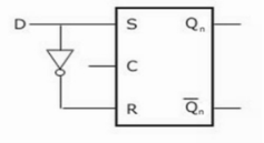
Ii) Convert SR To D Flip Flop:
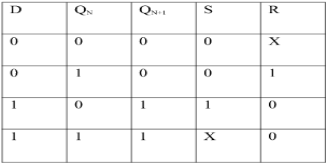
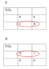
Excitation Functions:
S = D
R = D‘
There are basically 3 types of factors which affect the working of a flip-flop:
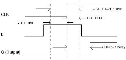
1. Setup time
2. Hold time
3. Propagation time
Setup Time: It is defined as minimum amount of time required for which an input should be stable just before the clock transition occurs.

Hold Time: It is defined as minimum amount of time required for which an input should be stable just after the clock transition occurs.

And both conditions can be represented as follow and inputs should be stable for at least 2 ns:

PROPAGATION TIME:
It is defined as the time after the clock transition, required for a flip-flop to generate output. This is also called CLOCK TO Q delay T clock-to-q.
e.g. Let’s draw the wave forms of inputs and outputs for D FLIP-FLOP which would illustrate the above discussed:
- Flip flops are used to store one bit of binary data (1or 0).
- If we need to store multiple bits of data, we use multiple flip flops.
- N flip flops are connected to store n bits of data.
- A Register is a device which stores such information. It is a group of flip flops connected in series which is used to store multiple bits of data.
- The information stored in these registers can be transferred with the help of shift registers.
- This register is a group of flip flops used to store multiple bits of data.
- The bits stored in these registers can be moved in/out of the registers by applying clock pulses.
- The registers which shift the bits towards left are called “Shift left registers”.
The registers which shift the bits towards right are called “Shift right registers”.
Shift registers are of 4 types and they are:
- Serial In Serial Out register
- Serial In parallel Out register
- Parallel In Serial Out register
- Parallel In parallel Out register
Applications Of Shift Registers
- They are used for temporary data storage.
- They are used for data transfer and data manipulation.
- The SISO and PIPO registers are used to produce time delay in digital circuits.
- The SIPO register is used for conversion of serial data to parallel data hence they are used in communication lines .
- A PISO register is used to convert parallel data to serial data.
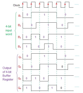
Buffer registers are a type of registers used to store a binary word. These can be constructed using a series of flip-flops as each flip-flop can store a single bit. This means that in order to store an n-bit binary word one should design an array of n flip-flops. Figure shows a 4-bit synchronous buffer register formed by cascading four positive edge triggered D flip-flops. Here the entire input data word B1B2B3B4 is loaded onto the register at a single clock tick. This means that at every leading edge of the clock the values of flip-flop outputs follow their input bits i.e. Q1 = B1, Q2 = B2, Q3 = B3 and Q4 = B4 as shown by Figure.

Fig.: 4 bit buffer register
Buffer registers offer no means of control over the inputs which in turn leads to uncontrolled outputs. In order to overcome this drawback one can resort to controlled buffer registers as shown by Figure.
In this design, tri-state switches are used to control the operation of loading and/or retrieval of the data to/from the buffer register. Here one has to pull the LD or WR control line (blue line) low in order to store the data into the register, while RD control line (red line) should be made low to read the data.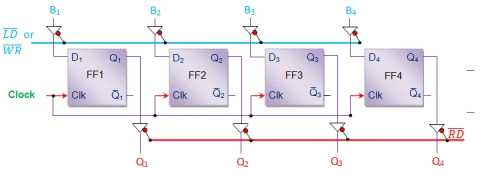
Fig.: 4 bit controlled buffer register
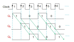
They are the devices which are used to store and/or shift the bits of the input data word. Here the data bits can be made to enter (or exit) the register in serial/parallel mode in synchronization with the clock pulse. Moreover the data bits within the shift register can be made to change their position by moving towards right or left for each clock pulse.
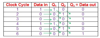
Serial-In Serial-Out Shift Register (SISO) –
- It allows serial input i.e., one bit after another and produces a serial output is known as Serial-In Serial-Out shift register.
- Since it has one output, the data leaves the register one bit at a time in a serial pattern, hence known as Serial-In Serial-Out Shift Register.
- The logic circuit is given underneath.
- The circuit comprises four D flip-flops which are connected serially.
- All these flip-flops are synchronous.

Fig. SISO
Serial-In Parallel-Out shift Register (SIPO) –
- It allows serial input through a single data line and produces a parallel output.
- The logic circuit is given underneath.
- The circuit consists of four D flip-flops which are connected synchronously.
- The clear (CLR) signal is also connected to all the 4 flip flops to RESET them.
- The output of the first flip flop is sent to the input of the next and so on.
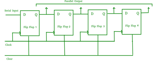
Fig. SIPO
- They are used in communication lines because the main use of the SIPO register is to convert serial data into parallel data.
Parallel-In Serial-Out Shift Register (PISO) –
- It allows parallel input data and produces a serial output.
- The logic circuit is given underneath.
- The circuit comprises four D flip-flops which are connected synchronously.
- The clock is connected to all the flip flops but the input data is connected to each flip flop individually through a multiplexer.
- The output of the previous flip flop and parallel data input are connected to the input of the MUX and the output of MUX is connected to the next flip flop.
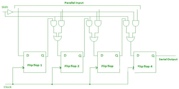
Fig. PISO
- It used to convert parallel data to serial data.
Parallel-In Parallel-Out Shift Register (PIPO) –
- It allows parallel input data and produces a parallel output.
- The logic circuit is given underneath.
- The circuit comprises four D flip-flops which are connected synchronously.
- The clear (CLR) and clock signals are connected to all flip flops.
- In this, there are no interconnections between flip-flops as no serial shifting of the data is required.
- Data is provided separately as input for each flip flop and the output is also collected individually from each flip flop.
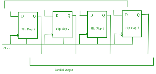
Fig. PIPO
- It is used as a temporary storage device and it acts as a delay element too.
- If a binary number is shifted towards left by one position, then it is equivalent to multiplying the number by 2 and if a binary number towards the right by one position, then it is equal to dividing the number by 2.
- To perform the above operations a register is used which can shift the data in either direction.
- Hence, Bidirectional shift registers are capable of shifting the data either right or left depending on the mode selected.
- If the mode =1(high), then the data is shifted towards the right, and if the mode = 0(low), then the data is shifted towards the left direction.
- The logic circuit is given underneath.
- The circuit comprises four D flip-flops which are connected synchronously.
- The input data is connected at two ends of the circuit and depending on the model and gate selected.
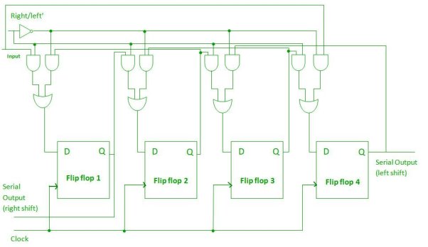
Fig. Bidirectional shift register
It is a register that has both the right shift and left shift with parallel load capabilities.
They are used as memory elements in computers.
It is capable of shifting in one direction.
It is capable of shifting in both directions.
It is a combination of a bidirectional and unidirectional shift register with parallel load provision.
n-bit universal shift register –
It comprises n flip-flops and n 4×1 multiplexers.
All the multiplexers share the same select lines (S1 and S0).
The select inputs select the suitable input for the flip-flops.
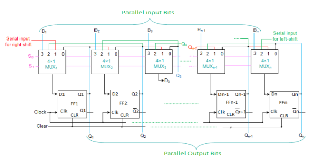
Fig. The N-bit universal shift register
S1 | S0 | REGISTER OPERATION |
0 | 0 | No changes |
0 | 1 | Shift right |
1 | 0 | Shift left |
1 | 1 | Parallel load |
A Counter stores the number of times a particular event or process has occurred in relationship to a clock signal.
They are used in digital electronics for counting purpose.
They can count specific event happening how many times in the circuit.
For example, in UP counter count increases for every rising edge of clock.
A counter can follow certain sequence based on our design like any sequence 0,1,3,2… .
They can be designed with the help of flip flops.
Counter Classification
Counters are broadly classified into two categories:
- Asynchronous counter
- Synchronous counter
1. Asynchronous Counter
In this universal clock is not used and only the first flip flop is driven by main clock and the clock input of rest of the following is driven by output of previous flip flops.

Fig. Asynchronous counter
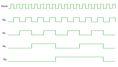
Fig. Timing diagram of Asynchronous counter
It is seen from timing diagram that Q0 is changing as soon as the rising edge of clock pulse is encountered.
Q1 is changing when rising edge of Q0 is encountered and so on.
In this way ripples are generated through Q0,Q1,Q2,Q3 and therefore it is also called as a RIPPLE counter.
2. Synchronous Counter
It has one global clock which drives each and every flip flop and hence output changes in parallel.
The advantage of synchronous counter over asynchronous counter is that it can operate on higher frequency and it does not have cumulative delay .
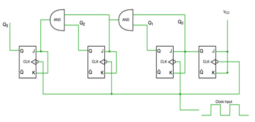
Fig. Synchronous counter
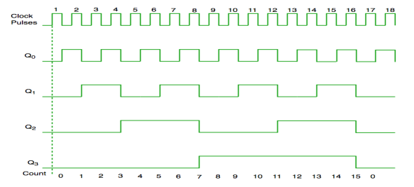
Fig. Timing diagram of synchronous counter
- In this universal clock is not used and only the first flip flop is driven by main clock and the clock input of rest of the following is driven by output of previous flip flops.

Asynchronous counter
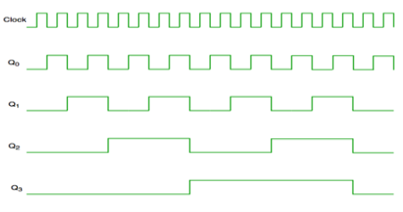
Timing diagram of Asynchronous counter
- It is seen from timing diagram that Q0 is changing as soon as the rising edge of clock pulse is encountered.
- Q1 is changing when rising edge of Q0 is encountered and so on.
- In this way ripples are generated through Q0,Q1,Q2,Q3 and therefore it is also called as a RIPPLE counter.
The problem with asynchronous counter is the "ripple".
Example: 4-bit asynchronous counter counting up. The transition from 0111 --> 1000 goes through or ripple through 3 intermediate states because of accumulation of propogation delays of each preceding Flip-Flop. These are glitches in the asynchronous counters.
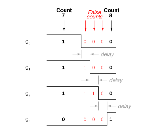
If some LEDs are pluged in at the 4-bit outputs of the counter, the glitch is not noticeable at all as these ripples are fast enough and it counts correctly. But if it is fed to some other digital logic for sampling, these glitches may cause unwanted errors.
Both Synchronous and Asynchronous counters are capable of counting “Up” or counting “Down”, but there is another more “Universal” type of counter that can count in both directions either up or down depending on the state of their input control pin and these are known as Bidirectional Counters.
Bidirectional counters, also known as Up/Down counters, are capable of counting in either direction through any given count sequence and they can be reversed at any point within their count sequence by using an additional control input as shown below.
The circuit above is of a simple 3-bit Up/Down synchronous counter using JK flip-flops configured to operate as toggle or T-type flip-flops giving a maximum count of zero (000) to seven (111) and back to zero again. Then the 3-Bit counter advances upward in sequence (0,1,2,3,4,5,6,7) or downwards in reverse sequence (7,6,5,4,3,2,1,0).
Generally, most bidirectional counter chips can be made to change their count direction either up or down at any point within their counting sequence. This is achieved by using an additional input pin which determines the direction of the count, either Up or Down and the timing diagram gives an example of the counter’s operation as this Up/Down input changes state.
Nowadays, both up and down counters are incorporated into single IC that is fully programmable to count in both an “Up” and a “Down” direction from any preset value producing a complete Bidirectional Counter chip. Common chips available are the 74HC190 4-bit BCD decade Up/Down counter, the 74F569 is a fully synchronous Up/Down binary counter and the CMOS 4029 4-bit Synchronous Up/Down counter.
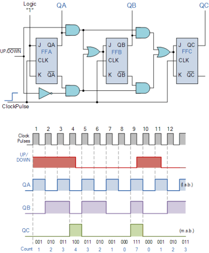
Fig: Up/Down Counter
Key takeaway
Both Synchronous and Asynchronous counters are capable of counting “Up” or counting “Down”, but there is another more “Universal” type of counter that can count in both directions either Up or Down depending on the state of their input control pin and these are known as Bidirectional Counters.
Mod-n counters
- It counts ten different states and then reset to its initial states.
- A simple decade counter will count from 0 to 9 but the decade counters which can go through any ten states between 0 to 15(for 4 bit counter) can also be made.
Truth table is as follows:
Clock pulse | Q3 | Q2 | Q1 | Q0 |
0 | 0 | 0 | 0 | 0 |
1 | 0 | 0 | 0 | 1 |
2 | 0 | 0 | 1 | 0 |
3 | 0 | 0 | 1 | 1 |
4 | 0 | 1 | 0 | 0 |
5 | 0 | 1 | 0 | 1 |
6 | 0 | 1 | 1 | 0 |
7 | 0 | 1 | 1 | 1 |
8 | 1 | 0 | 0 | 0 |
9 | 1 | 0 | 0 | 1 |
10 | 0 | 0 | 0 | 0 |
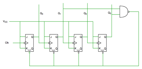
Fig. Decade counter
In the above circuit diagram we used nand gate for Q3 and Q1 and sending this to clear input line as the binary representation of 10 is—
1010
And Q3 and Q1 are 1 here, if we give NAND of these two bits then counter clears at 10 and again starts from the beginning.
- It has one global clock which drives each and every flip flop and hence output changes in parallel.
- The advantage of synchronous counter over asynchronous counter is that it can operate on higher frequency and it does not have cumulative delay
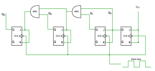
Synchronous counter
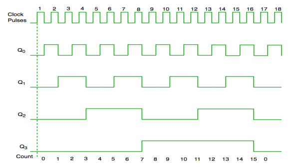
Timing diagram of synchronous counter
- It is a shift register counter whose output of the first flip flop is connected to the second and so on and the output of the last flip flop is fed back to the input of the first flip flop, thus named as ring counter.
- The data pattern in the register circulates as long as clock pulses are applied.
- The circuit below comprises of four D flip-flops which are connected synchronously.
- The data pattern repeats after every four clock pulses shown in the truth table.
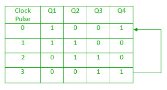

Fig. Ring counter
- It is self-decoding.
- Hence no extra decoding circuit is required to determine which state the counter is in.
Key takeaway
It is a shift register counter whose output of the first flip flop is connected to the second and so on and the output of the last flip flop is fed back to the input of the first flip flop, thus named as ring counter.
It is a shift register counter whose output of the first flip flop is connected to the second and so on and then an inverted output of the last flip flop is sent back to the first flip flop.
- They are also called as twisted ring counters.
- The circuit below consists of four D flip-flops which are connected synchronously.
- An n-stage Johnson counter provides a count sequence of 2n different states, thus also known as a mod-2n counter.
- Since the circuit has four flip flops, the data pattern will repeat every eight clock pulses which are shown in the truth table below:
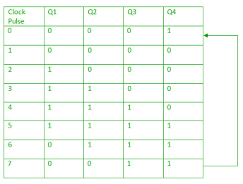
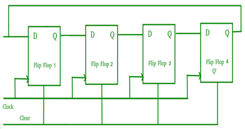
Fig. Johnson counter
- The main advantage is that it only needs n number of flip-flops to circulate a given data to generate a sequence.
A synchronous sequential circuit is also called as Finite State Machine FSM, if it has finite number of states. There are two types of FSMs.
- Mealy State Machine
- Moore State Machine
Mealy Machine
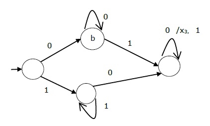
A Mealy Machine is an FSM whose output depends on the present state as well as the present input.
It can be described by a 6 tuple (Q, ∑, O, δ, X, q0) where −
- Q is a finite set of states.
- ∑ is a finite set of symbols called the input alphabet.
- O is a finite set of symbols called the output alphabet.
- δ is the input transition function where δ: Q × ∑ → Q
- X is the output transition function where X: Q × ∑ → O
- q0 is the initial state from where any input is processed (q0 ∈ Q).
The state table of a Mealy Machine is shown below −
Present state | Next state | |||
Input = 0 | Input = 1 | |||
State | Output | State | Output | |
→ a | b | x1 | c | x1 |
b | b | x2 | d | x3 |
c | d | x3 | c | x1 |
d | d | x3 | d | x2 |
The state diagram of the above Mealy Machine is −
Moore Machine
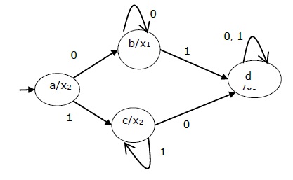
Moore machine is an FSM whose outputs depend on only the present state.
A Moore machine can be described by a 6 tuple (Q, ∑, O, δ, X, q0) where −
- Q is a finite set of states.
- ∑ is a finite set of symbols called the input alphabet.
- O is a finite set of symbols called the output alphabet.
- δ is the input transition function where δ: Q × ∑ → Q
- X is the output transition function where X: Q → O
- q0 is the initial state from where any input is processed (q0 ∈ Q).
The state table of a Moore Machine is shown below −
Present state | Next State | Output | |
Input = 0 | Input = 1 | ||
→ a | b | c | x2 |
b | b | d | x1 |
c | c | d | x2 |
d | d | d | x3 |
The state diagram of the above Moore Machine is −
Mealy Machine vs. Moore Machine
The following table highlights the points that differentiate a Mealy Machine from a Moore Machine.
Mealy Machine | Moore Machine |
Output depends both upon the present state and the present input | Output depends only upon the present state. |
Generally, it has fewer states than Moore Machine. | Generally, it has more states than Mealy Machine. |
The value of the output function is a function of the transitions and the changes, when the input logic on the present state is done. | The value of the output function is a function of the current state and the changes at the clock edges, whenever state changes occur. |
Mealy machines react faster to inputs. They generally react in the same clock cycle. | In Moore machines, more logic is required to decode the outputs resulting in more circuit delays. They generally react one clock cycle later. |
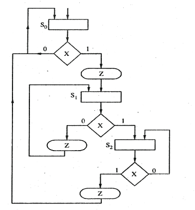
ASM stands for 'Algorithm State Machine 'or simply state machine is another name given to sequential network is used to control a digital system which carries out a step by a step –by step procedure. It should be noted that ASM charts represent physical hardware and offers several advantages.
1. Operation of a digital system can be easily understood by inspection of the SM chart.
2. ASM charts represent physical hardware.
3. The ASM chart are equivalent to a state graph, and it leads directly to a hardware realization.
4. ASM charts can be described the operation of both combinational and sequential circuits.
5. ASM charts are easier to understand and can be converted several equivalent forms.
6. The ASM chart may be equivalently expressed as a state and output table.
Following are the three basic components of ASM charts.
- State box
- Decision box
- Conditional output box
State box
State box is represented in rectangular shape. Each state box represents one state of the sequential circuit. The symbol of state box is shown in the following figure.
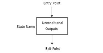
It is having one entry point and one exit point. Name of the state is placed to the left of state box. The unconditional outputs corresponding to that state can be placed inside state box. Moore state machine outputs can also be placed inside state box.
Decision box
Decision box is represented in diamond shape. The symbol of decision box is shown in the following figure.
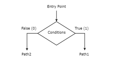
It is having one entry point and two exit paths. The inputs or Boolean expressions can be placed inside the decision box, which are to be checked whether they are true or false. If the condition is true, then it will prefer path1. Otherwise, it will prefer path2.
Conditional output box
Conditional output box is represented in oval shape. The symbol of conditional output box is shown in the following figure.
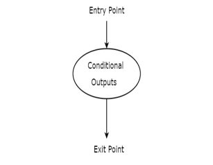
It is also having one entry point and one exit point similar to state box. The conditional outputs can be placed inside state box. In general, Mealy state machine outputs are represented inside conditional output box. So, based on the requirement, we can use the above components properly for drawing ASM charts.
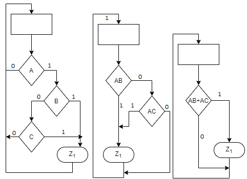
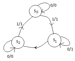
Example 1
Convert the state diagram of Fig. Below to ASM chart.
Sol:
References:
1. Rajkamal ‘Digital Systems Principals and Design’ Pearson Education
2. A.P. Malvino, D.P. Leach ‘Digital Principles & Applicatios’ -VIth Edition-TMH publication.
3. M. Morris Mano ‘Digital Design’ (Third Edition). PHI Publications