Unit - 5
Logic Families and VLSI Design flow
The circuit diagram of a 2 input TTL NAND gate is as follows:
A two input TTL NAND is shown above. A and B are two inputs while Y is the output.
Operation of the gate:
a) A and B both low: both B-E junctions of Q1 are forward biased. Hence D1 and D2 will conduct to force the voltage at point C to 0.7V. This voltage is insufficient to forward bias B-E junction of Q2. Hence Q2 remains OFF. Therefore, its collector voltage rises to VCCVCC. As Q3 is operating in emitter follower mode, output Y will be pulled up to high voltage Y= 1
b) Either A or B low: If any one input is connected to ground with other left open or connected to VCCVCC the corresponding diode (D1 or D2) will conduct. This will pull down voltage at C o 0.7V. This voltage is insufficient to turn on Q2 so it remains OFF. So, collector voltage of Q2 will be equal to VCC. This voltage acts as base voltage for Q3. As Q3 acts as an emitter follower, output Y will be pulled to VCCVCC. Y= 1
c) A and B both high: If both A and B are connected to then both diodes D1 and D2 will be reverse biased and do not conduct. Therefore, D3 is forward biased and base current is supplied to transistor Q2 via R1 and D3. As Q2 conducts, the voltage at X will drop down and Q3 will be OFF, whereas voltage at Z will increase to turn ON Q4. As Q4 goes into saturation, the output voltage Y will be pulled down to low. Y = 0
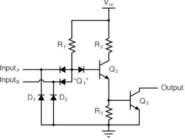
Fig: TTL NAND Gate
Specifications | TTL | CMOS |
Basic Gate | NAND | NOR/NAND |
Components | Passive Elements & Transistors | MOSFETs |
Fan-out | 10 | >50 |
Noise Immunity | Strong | Extremely Strong |
Noise Margin | Moderate | High |
TPD in ns | 1.5 to 30 | 1 to 210 |
Clock Rate in MHz | 35 | 10 |
Power/Gate in mW | 10 | 0.0025 |
Figure of Merit | 100 | 0.7 |
Gate circuits are made to sustain variations in input and output voltage levels.
Variations are usually the result of various factors.
- When Batteries lose their full potential, they cause the supply voltage to drop.
- High operating temperatures drifts transistor voltage and current characteristics.
- Spurious pulses on signal lines are introduced by normal surges of current in neighbouring supply lines.
- LNM (Low noise margin): LNM=VILmax-VOLmax.
- HNM (High noise margin): HNM=VOHmin-VIHmin
The time between the logic transition on an input and the corresponding logic transition on the output of the logic gate.
It is measured at midpoints.
- It is the number of inputs that a gate can have like a two input AND gate has fan-in of two, a three input NAND gate as a fan-in of three etc.
- Hence a NOT gate has a fan-in of one.
- The figure below shows the effect of fan-in on a CMOS based gate.
- Normally delay increases as a quadratic function of fan-in.
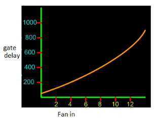
Fig: Effects of Fan-in
- The number of gates that each gate can drive, while providing voltage levels in the specified range is called the standard load or fan-out.
- It depends on the amount of electric current a gate can source or sink while driving other gates.
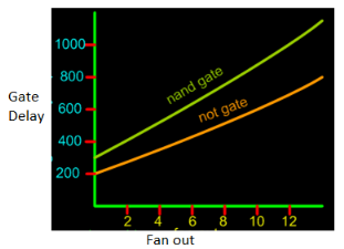
Fig: Effects of Fan-out
Transistor-transistor logic (TTL) is a class of integrated circuits that maintains logic states and switches with the help of bipolar transistors.
It inputs rise to the logic "1" if left unconnected. It is one of the reasons that integrated circuits are widely used, as they are cheap, reliable and faster than RTL and DTL.
TTL makes use of transistors with multiple emitters in gates having multiple inputs.
The family of TTL is as follows:
- Standard TTL
It is used for 3.3-volt power supplies and memory interfacing.
- Fast TTL
It has faster switching than (6ns) but significantly higher power dissipation (22 mW).
- Schottky TTL
It uses Schottky diode clamps at gate inputs to prevent charge storage and improve switching time.
- Low power Schottky TTL
It is used for high resistance values of low-power TTL and the Schottky diodes provide a good combination of speed (9.5ns) and reduce power consumption (2 mW) too.
- Low power TTL
It is traded switching speed (33ns) for a reduction in power consumption (1 mW).
- Advanced Schottky TTL
It speeds up the low-to-high transition of TTL.
Advantages
- It is relatively easy in interfacing different circuits and produce complex logic functions.
- It has good noise margins as well as guaranteed voltage levels.
- It has good fan-in and is largely immune to damage from static electricity discharges
Disadvantages
- It has limited speed, low frequency, very noisy, high power consumption at higher frequencies.
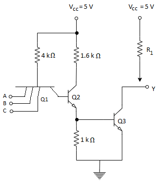
Fig: TTL
Key Takeaways:
- TTL is a standard method of construction for the processors of mini-computer and mainframe processors.
- TTL gate works as an analog amplifier.
Emitter Coupled Logic or ECL emitter-coupled logic (ECL) is a high-speed integrated circuit bipolar transistor logic family. ECL uses an overdriven BJT differential amplifier with single-ended input and limited emitter current to avoid the saturated (fully on) region of operation and its slow turn-off behavior.
Emitter Coupled Logic (ECL), also referred to as Current Mode Logic families, is a digital technology with extremely high-speed. Transistors are not allowed to go into deep saturation thus, eliminating storage delays like in TTL logic families.
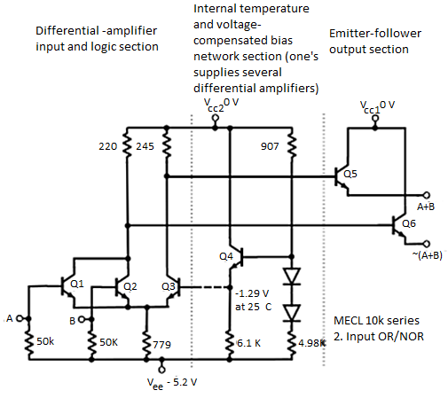
Fig: Motorola ECL 10,000 basic gate circuit diagram. Image source: Wikipedia
As the current is steered between two legs of an emitter-coupled pair, ECL is sometimes called current-steering logic (CSL), current-mode logic (CML)or current-switch emitter-follower (CSEF) logic.
ECL's major disadvantage is that each gate continuously draws current, which means that it requires (and dissipates) significantly more power than those of other logic families, especially when quiescent.
CMOS inverter
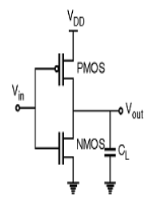
Fig: CMOS inverter
- It consists of PMOS and NMOS FET.
- The input A serves as the gate voltage for both transistors.
- The NMOS transistor has an input from Vss (ground) and PMOS transistor has an input from Vdd. The terminal Y is output.
- When a high voltage (~ Vdd) is given at input terminal (A) of the inverter, the PMOS becomes open circuit and NMOS switched OFF so the output will be pulled down to Vss.
- The truth table of inverter is:
A | Y = A’ |
0 | 1 |
1 | 0 |

Fig: NOT gate
CMOS characteristics
The VTC is divided into five regions (1-5) for easy of understanding. The above shown curve is possible when both T1 and T2 are matched for optimum operation. Optimum operation is achieved when Vin = Vdd/2 we get Vout = Vdd/2. This can be achieved by adjusting width and length of both T1 and T2 as other parameters like mobility, oxide capacitance varies between different technologies.
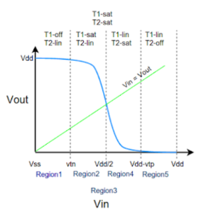
Fig: CMOS characteristics
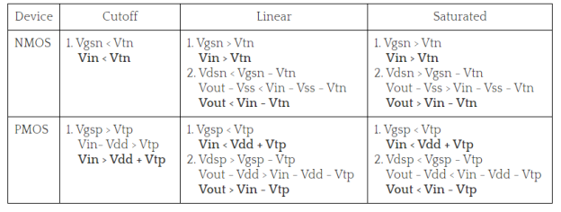
Region-1
In this, the input is in the range of (0, Vtn).
- NMOS is in cut-off as Vgs<Vtn
- PMOS is in linear as Vgsp<Vtp and Vdsp>Vgsp -Vtp.
- Zero current flows from supply voltage and the power dissipation is zero.
Region-2
Here, the input is in the range of (Vtn, Vdd/2).
- NMOS is in saturation as Vgs>Vtn and Vout>Vin – Vtn.
- PMOS is in linear region as Vdsp>Vgsp -Vtp.
- Since both the transistors are conducting some amount of current flows from supply in this region.
Region-3
Here the input voltage is Vdd/2. At this point the output voltage is Vdd/2. Here both the NMOS and PMOS are in saturation and the output drops drastically from Vdd to Vdd/2. At this point a large amount of current flows from the supply.
- NMOS is in saturation as Vgs>Vtn and Vout>Vin - Vtn.
- PMOS is in saturation as Vgsp<Vtp and Vdsp<Vgsp -Vtp.
- Large amount of current is drawn from supply and hence large power dissipation.
Region-4
In this region the input voltage is in the range of (Vdd/2, Vdd-Vtp). Here the PMOS remains in saturation as Vout< Vin - Vtp and Vgsp<Vtp. But the NMOS moves from saturation to linear region since the drain to source voltage now is less than Vgsn-Vtn.
- NMOS is in linear as Vgs>Vtn and Vout< Vin - Vtn.
- PMOS is in saturation as Vgsp<Vtp and Vdsp<Vgsp -Vtp.
- A medium amount of current is drawn as NMOS is in linear region and power dissipation is low.
Region-5
In this region the input voltage is in the range of (Vdd-Vtp, Vdd). Here the PMOS moves from saturation to cut-off as the Vgsp is so high that Vgsp>Vtp. The NMOS still remains in linear as the drain to source voltage now is less than Vgsn-Vtn.
- NMOS is in linear as Vgs>Vtn and Vout< Vin - Vtn.
- PMOS is in cut-off as Vgsp>Vtp.
- Zero current flows from the supply and hence the power dissipation is zero.
CMOS configurations- Wired Logic, Open-drain outputs
Open Drain is a type of programmable output port configuration with push pull, input only, and quasi-bidirectional configurations. Open-collector/open-drain is a circuit technique which allows multiple devices to communicate bidirectionally on a single wire. This is basically a mode which provides just a pull-down operation.
An open collector/open drain is a common type of output found on many integrated circuits (IC). Instead of outputting a signal of a specific voltage or current, the output signal is applied to the base of an internal NPN transistor whose collector is externalized (open) on a pin of the IC. The emitter of the transistor is connected internally to the ground pin. If the output device is a MOSFET the output is called open drain and it functions in a similar way.
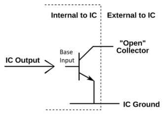
Fig: CMOS
CMOS driving TTL:
Following figure shows a CMOS gate driving N TTL gates. For such an arrangement to operate properly the following conditions are required to be satisfied,
VOH (CMOS) ≥ VIH(TTL)
VOL (CMOS) ≤ VIL(TTL)
– IOH (CMOS) ≥ NIIH(TTL)
IOL (CMOS) ≥ – NIIL(TTL)
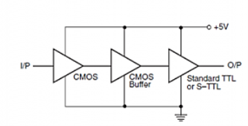
The first possible type of CMOS-to-TTL interface is the one where both ICs are operated from a common supply. We have read in earlier sections that the TTL family has a recommended supply voltage of 5 V, whereas the CMOS family devices can operate over a wide supply voltage range of 3†“18 V. In the present case, both ICs would operate from 5 V. As far as the voltage levels in the two logic states are concerned, the two have become compatible. The CMOS output has a VOH (min.) of 4.95V (for VCC =5 V) and a VOL (max.) of 0.05 V, which is compatible with VIH (min.) and VIL (max.) requirements of approximately 2 and 0.8V respectively for TTL family devices. In fact, in a CMOS-to- TTL interface, with the two devices operating on the same VCC, voltage level compatibility is always there. It is the current level compatibility that needs attention. That is, in the LOW state, the output current-sinking capability of the CMOS IC in question must at least equal the input current-sinking requirement of the TTL IC being driven. Similarly, in the HIGH state, the HIGH output current drive capability of the CMOS IC must equal or exceed the High-level input current requirement of TTL IC. For a proper interface, both the above conditions must be met. As a rule of thumb, a CMOS IC belonging to the 4000B family (the most widely used CMOS family) can feed one LS TTL or two low-power TTL unit loads. When a CMOS IC needs to drive a standard TTL or a Schottky TTL device, a CMOS buffer (4049B or 4050B) is used. 4049B and 4050B are hex buffers of inverting and noninverting types respectively, with each buffer capable of driving two standard TTL loads.
Figure below shows a CMOS-to-TTL interface with both devices operating from 5V supply and the CMOS IC driving a low-power TTL or a low-power Schottky TTL device.
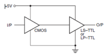
Figure below shows a CMOS-to-TTL interface where the TTL device in use is either a standard TTL or a Schottky TTL.
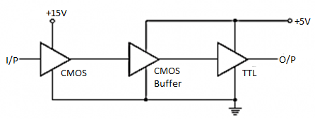
The CMOS-to-TTL interface when the two are operating on different power supply voltages can be achieved in several ways. One such scheme is shown below. In this case, there is both a voltage level as well as a current level compatibility problem.
TTL Driving CMOS:
For TTL gate driving N CMOS gates arrangement to operate properly, the following conditions are required to be satisfied:
VOH (TTL) ≥ VIH(CMOS)
VOL (TTL) ≤ VIL(CMOS)
– IOH (TTL) ≥ NIIH(CMOS)
IOL (TTL) ≥ – NIIL(CMOS)
In the TTL-to-CMOS interface, current compatibility is always there. The voltage level compatibility in the two states is a problem. VOH (min.) of TTL devices is too low as regards the VIH (min.) requirement of CMOS devices. When the two devices are operating on the same power supply voltage, that is, 5 V, a pull-up resistor of 10 k_ achieves compatibility as shown in below figure.
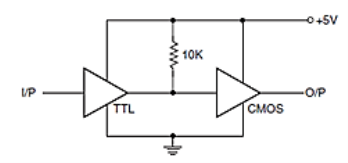
The pull-up resistor causes the TTL output to rise to about 5V when HIGH. When the two are operating on different power supplies, one of the simplest interface techniques is to use a transistor (as a switch) in-between the two, as shown below.
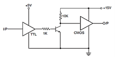
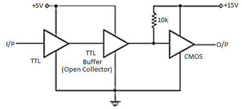
Another technique is to use an open collector type TTL buffer as shown below.
The memory is organized in the form of a cell, each cell is able to be identified with a unique number called address. Each cell is able to recognize control signals such as “read” and “write”, generated by CPU when it wants to read or write address. Whenever CPU executes the program there is a need to transfer the instruction from the memory to CPU because the program is available in memory. To access the instruction CPU generates the memory request.
Memory Request:
Memory request contains the address along with the control signals. For Example, when inserting data into the stack, each block consumes memory (RAM) and the number of memory cells can be determined by the capacity of a memory chip.
Example: Find the total number of cells in 64k*8 memory chip.
Size of each cell = 8
Number of bytes in 64k = (26)*(210)
Therefore,
The total number of cells = 216 cells
With the number of cells, the number of address lines required to enable one cell can be determined.
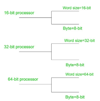
Word Size:
It is the maximum number of bits that a CPU can process at a time and it depends upon the processor. Word size is a fixed size piece of data handled as a unit by the instruction set or the hardware of a processor.
Memory can be classified as –
- Main Memory– Main memory has the disadvantage of high-cost and low-capacity storage. But its advantage or facility is the high speed of data transfer. The control unit can be able to directly communicate with the main memory. Main memory can be generally classified into random-access memory (RAM) and read-only memory (ROM). It is a volatile memory. Due to the absence of power, the content of this memory will be lost.
- Secondary Memory– Secondary memory is also frequently known as auxiliary memory. The control unit can’t directly communicate with the secondary memory. It is a non-volatile memory.
Random Access Memory (RAM) – RAM contains of a various number of memory locations wherein each location typically 8-bits are stored. It can be possible to read from a RAM location, as well as write to a RAM location. The drawback of RAM is that it is volatile. That means, when the power supply to the RAM is switched off, the information in the RAM will be lost.
From the memory, data can be accessed in two different ways – Sequential Access and Random Access.
Sequential Access − Sequential access and random access are two types of accessing information. In sequential access, it is mandatory to access information strictly in order. If there are 4000 memory locations, it has to be accessed in the order of 1, 2, 3…,4000. Thus, it takes minimum time to access information from location 0 and at most time to access information from location 4000. Magnetic Tape is an example that employs sequential access.
Random Access − In a random-access technique, it can be possible to access a memory location in any order. For example, one can read from the 4000locations in the order of 1500, 1210, 3060, 1640, 1352, and so on. Second, it takes a similar time to read from a memory location irrespective of its position. In a RAM, the access method is random, and its name, in fact, is derived based on the method of access.
Read Only Memory (ROM) – ROM consists of a number of memory locations wherein each location typically 8-bits are stored like a RAM. A ROM also uses random access method just like a RAM. The advantage of ROM is that it is non-volatile in nature.
The different versions of ROM which are provided by semiconductor manufacturers for storing information –
Mask-Programmed ROM – It derives this name because the information is written to this type of ROM at the time of manufacture by applying a suitable mask. Once the manufacturer writes this type of ROM, it cannot be possible to change this information even by the manufacturer. So that the information entered is permanent. It is cheap with compared to the other types of ROMs when the cost per unit quantity is considered.
Programmable Read Only Memory (PROM) – The user writes information to this type of ROM with the help of PROM programmer equipment. Once the user writes this type of ROM, it cannot be possible to change this information anymore. Like Mask-Programmed ROM, the information entered is permanent. Though itis cheaper than the other types of ROMs but it is costlier than a mask ROM. The user can buy even a single piece of PROM from a local shop. Thus, PROMs are implemented in equipment those are produced in small quantities.
Erasable Programmable Read Only Memory (EPROM) – Information is written to this type of ROM by the user with the help of EPROM programmer equipment. As its content is erasable and rewritable, so the user can change this information in a number of times. Thus, although the information entered is not lost when power is switched off, it can be possible to erase it and then write new information. With the exposure of strong ultraviolet (UV) light from a very close distance on the quartz window of the EPROM chip, we can erase the content of the EPROM. Then the contents of the entire EPROM are entirely lost. The user can purchase even a single piece of EPROM from the market read and write its content for several numbers of times as well.
Electrically erasable (or Alterable) Programmable Read Only Memory (EEPROM or EEPROM) − Information is has written to this type of ROM by the user with the help of EPROM programmer equipment. After the user writes this type of ROM, it can be possible to change this information a number of times.
FPGAs are based on gate array technology unlike the PROM technology of early PLDs. These devices comprise of configurable logic blocks (CLBs) along with an interconnection matrix running in-between. FPGAs work based upon the look-up tables (LUTs) and the flip-flops which form a part of CLB. The user has to program the CLBs to perform a certain logical function and then use the interconnection matrix to connect one or more logic blocks together. Further, they comprise of input-output (I/O) ports facilitating the design both from the point of programming as well as debugging.
These devices are capable of implementing state-machine based sequential designs along with the designs based on combinational logic. FPGAs are used to realize more complex designs when compared to CPLDs due to their high density. Moreover, FPGAs offer the customer the flexibility to design/re-design the logic even after being deployed in the work field which gives them the name field-programmable.
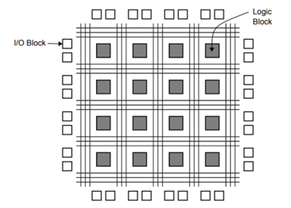
Fig: Architecture of FPGA
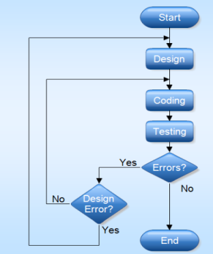


The first step in writing the VHDL for this FSM is to define the VHDL entity. The VHDL entity describes the external interface of the system you are designing which includes the inputs, the outputs, and the name of the entity.
The name of the entity will be Simple FSM, the inputs are a clock signal, the reset signal and the P signal, and the output is the R signal. It should be mentioned that the clock signal is the periodic high-low signal that controls the timing to this synchronous system. Any synchronous system has one controlling clock signal that synchronizes all of the blocks in the system making them change at the same time.
The next step is to define the functionality of the entity; this block of VHDL is called the architecture. The functionality that we are implementing is that of the state machine defined in figure 1. The example below shows the code that would be needed to implement the Simple FSM. While this code is specific to the Simple FSM, I will describe what each of the sections of the code do so that it will be an easy process to replace this code with code for your own state machine.
There are 3 types of modeling styles:
- Dataflow
- Behavioral
- Structural
Structural Modeling
In this an entity is described as a set of interconnected component .
Such a model is described with the help of code:
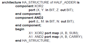
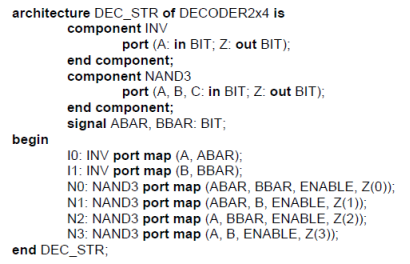
A structural representation of 2X4 decoder is given by:
Data Flow Modeling
Here, the flow of data through the entity is expressed using concurrent signal assignments.
The structure of the entity is not specified.
Such a model is described with the help of code:

A dataflow representation of 2X4 decoder is given by:
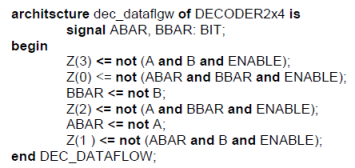
Behavioral Modeling
It specifies the behavior of the entity as a set of statements that are executed sequentially in a particular manner.
These statements are specified under a process statement.
A process statement can appear inside an architecture body only.
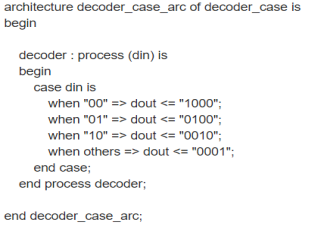
There are four types of data objects in VHDL:
- Signals
- Variables
- Constants
- Files
Signal
The signal represents interconnection wires between ports it may be declared in the declaration part of
- Packages
- Entities
- Architectures
- Blocks
The signal declaration is
Signal signal_name: signal_type;
Signal assignment: <=
Variable
The variable locally stores temporary data and it is used only inside a sequential statement that means
- Process
- Function
- Procedures
The variable is visible only inside processes and subprograms in which it is declared. The variable declaration is
Variable variable_name : variable_type;
Variable assignment: :=
Constant
The constant names specific values to make the model better documented and easy to update.
The constant can be declared in all the declarative VHDL statement,
- Sequential
- Concurrent
That means it may be declared in the declaration section of packages, entities, architectures, processes, subprograms and blocks
The constant declaration is
Constant constant_name : constant_type := value;
File
The File type is used to access File on disk.
It is used only in test bench; in fact File type cannot be implemented in hardware.
In order to use the FILE type you shall include the TextIO package that contains all procedures and functions that allow you to read from and write to formatted text files.
Input ASCII files are handled as file of lines, where a line is a string, terminated by a carriage return.
TextIO package declares a type line used to hold
- a line read from an input file
- a line to write to an output file
Process_write_file : process(...)
File file_name_write : text; -- declare file
Variable row : line; -- line to access file
Variable integer_value : integer; -- integer value write to file
Begin
-- open file write mode
File_open(file_name_read, “file_to_write.txt”, write_mode);
-- read line from file and then read integer value
Writeline(file_name_write,row);
Write(row,integer_value);
...
End process process_write_file;
Here, the flow of data through the entity is expressed using concurrent signal assignments.
The structure of the entity is not specified.
Such a model is described with the help of code:

A dataflow representation of 2X4 decoder is given by:

Structural Modeling
In this an entity is described as a set of interconnected components.
Such a model is described with the help of code:

A structural representation of 2X4 decoder is given by:

Behavioral Modeling
It specifies the behavior of the entity as a set of statements that are executed sequentially in a particular manner.
These statements are specified under a process statement.
A process statement can appear inside an architecture body only.

Example: For half adder
Library ieee;
Use ieee.std_logic_1164.all;
Entity half_adder_simple_tb is
End half_adder_simple_tb;
Architecture tb of half_adder_simple_tb is
Signal a, b : std_logic; -- inputs
Signal sum, carry : std_logic; -- outputs
Begin
-- connecting testbench signals with half_adder.vhd
UUT : entity work.half_adder port map (a => a, b => b, sum => sum, carry => carry);
-- inputs
-- 00 at 0 ns
-- 01 at 20 ns, as b is 0 at 20 ns and a is changed to 1 at 20 ns
-- 10 at 40 ns
-- 11 at 60 ns
a <= '0', '1' after 20 ns, '0' after 40 ns, '1' after 60 ns;
b <= '0', '1' after 40 ns;
End tb;
Program 1
Write a code for 4:1 MUX.
Library IEEE;
Use IEEE.STD_LOGIC_1164.ALL;
Use IEEE.STD_LOGIC_ARITH.ALL;
Use IEEE.STD_LOGIC_UNSIGNED.ALL;
Entity MUX_SOURCE is
Port ( S : in STD_LOGIC_VECTOR (1 downto 0);
I : in STD_LOGIC_VECTOR (3 downto 0);
Y : out STD_LOGIC);
End MUX_SOURCE;
Architecture Behavioral of MUX_SOURCE is
Begin
Process (S,I)
Begin
If (S <= "00") then
Y <= I(0);
Elsif (S <= "01") then
Y <= I(1);
Elsif (S <= "10") then
Y <= I(2);
Else
Y <= I(3);
End if;
End process;
End Behavioral;
Program 2
Write a code for full adder.
Library IEEE;
Use IEEE.STD_LOGIC_1164.ALL;
Use IEEE.STD_LOGIC_ARITH.ALL;
Use IEEE.STD_LOGIC_UNSIGNED.ALL;
Entity FULLADDER_BEHAVIORAL_SOURCE is
Port ( A : in STD_LOGIC_VECTOR (2 downto 0);
O : out STD_LOGIC_VECTOR (1 downto 0));
End FULLADDER_BEHAVIORAL_SOURCE;
Architecture Behavioral of FULLADDER_BEHAVIORAL_SOURCE is
Begin
Process (A)
Begin
—for SUM
If (A = “001” or A = “010” or A = “100” or A = “111”) then
O(1) <= ‘1’;
—single inverted commas used for assigning to one bit
Else
O(1) < = ‘0’;
End if;
—for CARRY
If (A = “011” or A = “101” or A = “110” or A = “111”) then
O(0) <= ‘1’;
Else
O(0) <<= ‘0’;
End if;
End process;
End Behavioral;
Program 3
Write a code for
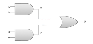
Library IEEE;
Use IEEE.STD_LOGIC_1164.ALL;
Use IEEE.STD_LOGIC_ARITH.ALL;
Use IEEE.STD_LOGIC_UNSIGNED.ALL;
Entity and_or is
Port(
a : in std_logic;
b : in std_logic;
d : in std_logic;
e : in std_logic;
g : out std_logic);
End and_or;
Architecture and_or_a of and_or is
-- declarative part: empty
Begin
g <= (a and b) or (d and e);
End and_or_a;
Program 4
Write a code for JK flip-flop.
Library IEEE;
use IEEE.STD_LOGIC_1164.all;
entity jk is
port(
j : in STD_LOGIC;
k : in STD_LOGIC;
clk : in STD_LOGIC;
reset : in STD_LOGIC;
q : out STD_LOGIC;
qb : out STD_LOGIC
);
end jk;
architecture jk_flip_flop of jk is
begin
jkff : process (j,k,clk,reset) is
variable m : std_logic := '0';
begin
if (reset='1') then
m := '0';
elsif (rising_edge (clk)) then
if (j/=k) then
m := j;
elsif (j='1' and k='1') then
m := not m;
end if;
end if;
q <= m;
qb <= not m;
end process jkff;
end jk_flip_flop;
Program 5
Write a code for RS latch.
Library IEEE;
use IEEE.STD_LOGIC_1164.all;
entity SR_Latch is
port(
enable : in STD_LOGIC;
s : in STD_LOGIC;
r : in STD_LOGIC;
reset : in STD_LOGIC;
q : out STD_LOGIC;
qb : out STD_LOGIC );
end SR_Latch;
architecture SR_Latch_arc of SR_Latch is
begin
latch : process (s,r,enable,reset) is
begin
if (reset='1') then
q <= '0';
qb <= '1';
elsif (enable='1') then
if (s/=r) then
q <= s;
qb <= r;
elsif (s='1' and r='1') then
q <= 'Z';
qb <= 'Z';
end if;
end if;
end process latch;
end SR_Latch_arc;
Program 6
Write a VHDL code for Mealy machine.
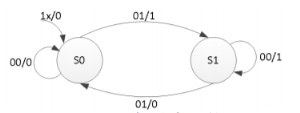
Type state_type is (S0, S1);
Signal state, next_state : state_type;
Begin
SYNC_PROC : process (clk)
Begin
If rising_edge(clk) then
If (reset = '1') then
State <= S0;
Else state <= next_state;
End if;
End if;
End process;
NEXT_STATE_DECODE : process (state, x)
Begin
Parity <= '0';
Case (state) is
When S0 =>
If (x = '1') then
Parity <= '1';
Next_state <= S1;
Else
Next_state <= S0;
End if;
When S1 =>
If (x = '1') then
Next_state <= S0;
Else
Parity <= '1';
Next_state <= S1;
End if;
When others =>
Next_state <= S0;
End case;
End process;
Program 7
Write a VHDL code for Moore machine.
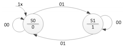
Type state_type is (S0, S1);
Signal state, next_state : state_type;
Begin
SYNC_PROC : process (clk)
Begin
If rising_edge(clk) then
If (reset = '1') then
State <= S0;
Else
State <= next_state;
End if;
End process;
OUTPUT_DECODE : process (state)
Begin
Case (state) is
When S0 =>
Parity <= '0';
When S1 =>
Parity <= '1';
When others =>
Parity <= '0';
End case;
End process;
NEXT_STATE_DECODE : process (state, x)
Begin
Next_state <= S0;
Case (state) is
When S0 =>
If (x = '1') then
Next_state <= S1;
End if;
When S1 =>
If (x = '0') then
Next_state <= S1;
End if;
When others => next_state <= S0;
End case;
End process;
References:
1. Rajkamal ‘Digital Systems Principals and Design’ Pearson Education
2. A.P. Malvino, D.P. Leach ‘Digital Principles & Applications’ -VIth Edition-TMH publication.
3. M. Morris Mano ‘Digital Design’ (Third Edition). PHI Publications