Unit - 1
Basic Electronic Components
Electronic systems are built around analog and digital components. They comprise resistors, capacitors, diodes, inductor, operational amplifiers and transistors. These components are often called active and passive elements. Majority of the analog circuits consist passive and active ones that are responsible for power management.
What is an Active element?
Active components control the charge flow in electronic circuits. It is the core component to operate any device. The two parameters to consider for proper device operation are current and voltage. Hence the voltage and current in a circuit may be boosted or stepped down based on the flow of electrons injected by an active device. Components like Diodes, Transistors, voltage operated devices, Vacuum tubes, voltage and current sources comes under active elements. An active component without doubt, amplifies the power of a signal (voltage or current). Transistor is a good example that acts as an amplifier in radio and RF circuits.
In addition, active elements are categorised into two sections. They are voltage controlled and current controlled sources. Voltage controlled devices produce their output current depending upon the input voltage. BJT (Bipolar junction transistor) is a voltage controlled device which supplies static voltage as a control signal.
What is Passive element?
Passive elements are quite opposite to active ones. They don’t require any external voltage to perform their job. Examples: Resistor, Capacitor, Inductor etc.
But they are not capable to provide energy on their own. They require assistance from active devices. For example, a resistor is a versatile component used as pull up or pulls down resistor in most of the hardware design.
We can use the pull-up and pull-down as control signal from the microcontroller interrupt to turn and turn off external devices. Inductors and capacitors have the capability to store energy for longer time and discharge.
Key takeaway
S.No. | Active Element | Passive Element |
1 | They require external power supply to operate | They do not require external power supply to operate |
2 | They have a function of gain | They do not have a function of gain |
3 | They produce energy in the form of voltage or current | They store energy in the form of voltage or current |
4 | Examples: Semiconductors, diodes and transistors | Examples: Resistor, capacitor and inductors |
There are many thousands of different Types of Resistors and are produced in a variety of forms because their particular characteristics and accuracy suit certain areas of application, such as High Stability, High Voltage, High Current etc, or are used as general-purpose resistors where their characteristics are less of a problem.
Some of the common characteristics associated with the resistor are; Temperature Coefficient, Voltage Coefficient, Noise, Frequency Response, Power as well as a resistors Temperature Rating, Physical Size and Reliability.
All modern fixed value resistors can be classified into four broad groups:
- Carbon Composition Resistor – Made of carbon dust or graphite paste, low wattage values.
- Film or Cermet Resistor – Made from conductive metal oxide paste, very low wattage values
- Wire-wound Resistor – Metallic bodies for heatsink mounting, very high wattage ratings
- Semiconductor Resistor – High frequency/precision surface mount thin film technology
Carbon Resistors are the most common type of Composition Resistors. Carbon resistors are a cheap general purpose resistor used in electrical and electronic circuits. Their resistive element is manufactured from a mixture of finely ground carbon dust or graphite (similar to pencil lead) and a non-conducting ceramic (clay) powder to bind it all together.
The Carbon Composite Resistor is a low to medium type power resistor which has a low inductance making them ideal for high frequency applications but they can also suffer from noise and stability when hot. Carbon composite resistors are generally prefixed with a “CR” notation (eg, CR10kΩ ) and are available in E6 ( ± 20% tolerance (accuracy) ), E12 ( ± 10% tolerance) and E24 ( ± 5% tolerance) packages with power ratings from 0.250 or 1/4 of a Watt up to 5 Watts.
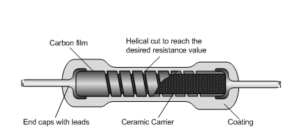
Fig 1 Carbon composite resistor
Film Type Resistors
This resistor consists of Metal Film, Carbon Film and Metal Oxide Film resistor types, which are generally made by depositing pure metals, such as nickel, or an oxide film, such as tin-oxide, onto an insulating ceramic rod or substrate.
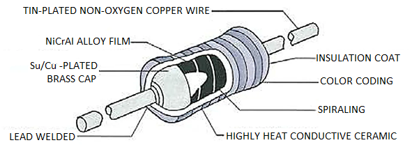
Fig 2 Film Resistor
The resistive value of the resistor is controlled by increasing the desired thickness of the deposited film giving them the names of either “thick-film resistors” or “thin-film resistors”. Once deposited, a laser is used to cut a high precision spiral helix groove type pattern into this film. The cutting of the film has the effect of increasing the conductive or resistive path, a bit like taking a long length of straight wire and forming it into a coil.
Metal Film Resistors have much better temperature stability than their carbon equivalents, lower noise and are generally better for high frequency or radio frequency applications. Metal Oxide Resistors have better high surge current capability with a much higher temperature rating than the equivalent metal film resistors.
Another type of film resistor commonly known as a Thick Film Resistor is manufactured by depositing a much thicker conductive paste of CERamic and METal, called Cermet, onto an alumina ceramic substrate.
Metal Film Resistors are prefixed with a “MFR” notation (eg, MFR100kΩ) and a CF for Carbon Film types. Metal film resistors are available in E24 (±5% & ±2% tolerances), E96 (±1% tolerance) and E192 (±0.5%, ±0.25% & ±0.1% tolerances) packages with power ratings of 0.05 (1/20th) of a Watt up to 1/2 Watt.
Wire wound Type of Resistor
Another type of resistor, called a Wire wound Resistor, is made by winding a thin metal alloy wire (Nichrome) or similar wire onto an insulating ceramic former in the form of a spiral helix similar to the film resistor above.
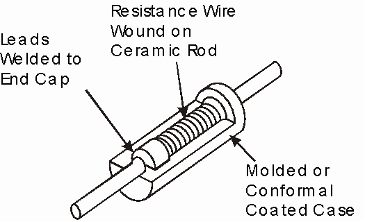
Fig 3 Wire wound Resistor
These types of resistors are generally only available in very low ohmic high precision values (from 0.01Ω to 100kΩ) due to the gauge of the wire and number of turns possible on the former making them ideal for use in measuring circuits and Wheatstone bridge type applications.
Wire wound resistor types are prefixed with a “WH” or “W” notation (eg WH10Ω) and are available in the WH aluminium clad package (±1%, ±2%, ±5% and ±10% tolerance) or the W vitreous enamelled package (±1%, ±2% and ±5% tolerance) with power ratings from 1W to 300W or more.
Calculating Resistor Values by colour Code
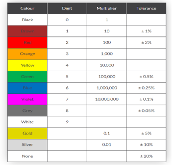
The Resistor Colour Code system is all well and good but we need to understand how to apply it in order to get the correct value of the resistor. The “left-hand” or the most significant coloured band is the band which is nearest to a connecting lead with the colour coded bands being read from left-to-right as follows:
Digit, Digit, Multiplier = Colour, Colour x 10 colour in Ohm’s (Ω)
For example, a resistor has the following coloured markings;
Yellow Violet Red = 4 7 2 = 4 7 x 102 = 4700Ω or 4k7 Ohm.
The fourth and fifth bands are used to determine the percentage tolerance of the resistor. Resistor tolerance is a measure of the resistors variation from the specified resistive value and is a consequence of the manufacturing process and is expressed as a percentage of its “nominal” or preferred value.
Typical resistor tolerances for film resistors range from 1% to 10% while carbon resistors have tolerances up to 20%. Resistors with tolerances lower than 2% are called precision resistors with the or lower tolerance resistors being more expensive.
Most five band resistors are precision resistors with tolerances of either 1% or 2% while most of the four band resistors have tolerances of 5%, 10% and 20%. The colour code used to denote the tolerance rating of a resistor is given as:
Brown = 1%, Red = 2%, Gold = 5%, Silver = 10 %
If resistor has no fourth tolerance band then the default tolerance would be at 20%
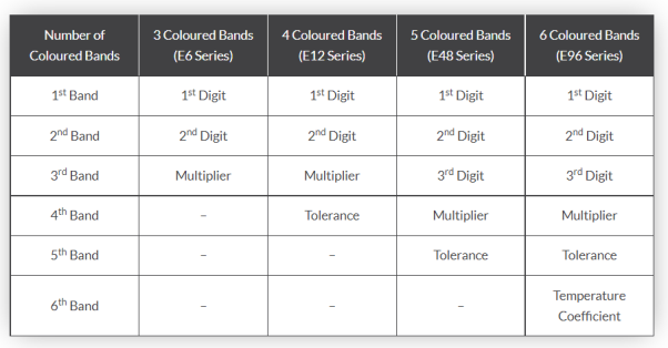
Resistor Colour Code Table
Capacitor is a charge storing device (voltage)
Q ∝ V
Q = C V


AC circuit with a pure capacitance
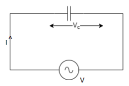
Fig 4 Circuit with pure Capacitance
Consider an AC circuit with a pure capacitance C as shown in the figure. The alternating voltage v is given by
V = Vm Sin ωt
 = Vm
= Vm  00
00
We can find the current through the capacitor as follows
q=CV
q= Cvm Sin ωt
 = ωCvm cos(ωt)
i= ωCvm cos(ωt)
i=im sin ( t+
t+ )
)
im= ωCvm
Xc = vm/im = 1/ωC
We observe that in a pure capacitive circuit, the current leads the voltage by 90⁰. Hence the voltage and current waveforms and phasors can be drawn as below.
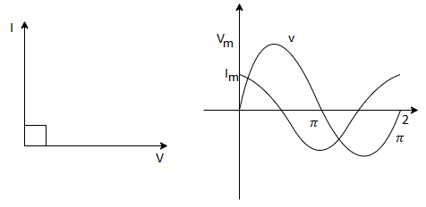
Fig 5 Phasor for C
Capacitive reactance
The capacitive reactance XC is given as
Xc= 1/2πfC
im = vm/Xc
Based on electromagnetic induction
Faraday’s Law

Φ∝i
Φ = L.i


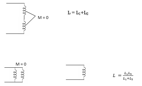
AC circuit with a pure inductance
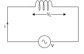
Fig 6 Circuit with pure inductance
Consider an AC circuit with a pure inductance L as shown in the figure. The alternating voltage v is given by
V = Vm Sin ωt
The current flowing in the circuit is i. The voltage across the inductor is given as VL which is the same as v. We can find the current through the inductor as follows
I=L 
Vm Sin ωt= L 
Di= Sin ωt
i = 

i =  sin (
sin ( t-
t- )
)
i= im sin ( t-
t- )
)
im = 
We observe that in a pure inductive circuit, the current lags behind the voltage by 90⁰. Hence the voltage and current waveforms and phasors can be drawn as below
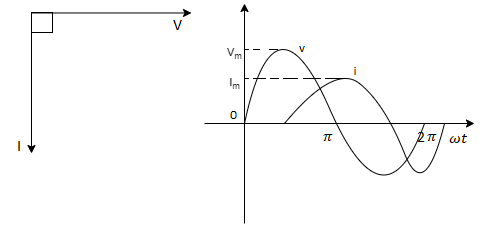
Fig 7 Phasor for Pure L
Inductive reactance
The inductive reactance XL is given as
XL = 2πfL
im = 
Key takeaway
Inductor do not respond any change as far as current is concerned.
Capacitor does not respond any change as far as voltage is concerned.
The applications of Resistor, capacitor and Inductor are mentioned below
Filters: Inductors, combined with capacitors and resistors, are used extensively to create filters for analogue circuits and in-signal processing. When inductors are used alone, they function as a low-pass filter. But when capacitors, inductors and resistors are used together, they operate as advanced filters that can be used in multiple applications.
Motors: Inductors are placed in a fixed position, and cannot be moved or aligned in nearby magnetic fields. Induction motors change the electrical energy into mechanical energy. The magnetic field produced by the alternating current helps to rotate the shaft in the motors.
Transformers: This is a popular application. Inductors that share the magnetic path are combined together and form a transformer.
Energy storage: Inductors can be used for energy storage. Unlike capacitors, they do not store energy for a long time. In the case of inductors, energy is stored in the form of the magnetic field; however, this fails when there is no power supply.
A relay comprises of an electromagnet and a contact unit. Activating the contact unit using electromagnetic attraction, which is produced when electric current exceeding the specified value flows to the electromagnet; the voltage and current (input signal) applied to the coil opens or shuts the contact. Relays used for
- As interfaces between control circuits and load circuits,
- For signal multiplication,
- For separation of direct current and alternating current circuits
- Linking information.
The working principle of the Solid Static relays is similar to that of the Electromechanical Relay which means the Solid Static relays can perform tasks that the Electromechanical Relay can perform. The Solid Static relays use analogue electronic devices instead of magnetic coils and mechanical components to create the relay characteristics. The measurement is carried out by static circuits consisting of comparators, level detectors, filter etc while in a conventional electro-magnetic relay it is done by comparing operating torque (or force) with restraining torque (or force). The relaying quantity such as voltage/current is rectified and measured. When the quantity under measurement attains certain well-defined value, the output device is triggered and thereby the circuit breaker trip circuit is energized.
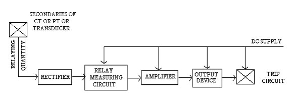
Fig 8 Static Relay
The essential components of static relays are shown in fig. The output of CT and PT are not suitable for static components so they are brought down to suitable level by auxiliary CT and PT. Then auxiliary CT output is given to rectifier. Rectifier rectifies the relaying quantity i.e., the output from a CT or PT or a Transducer.
The rectified output is supplied to a measuring unit comprising of comparators, level detectors, filters, logic circuits. The output is actuated when the dynamic input (i.e., the relaying quantity) attains the threshold value. This output of the measuring unit is amplified by amplifier and fed to the output unit device, which is usually an electro-magnetic one. The output unit energizes the trip coil only when relay operates.
Advantages of Solid-State Relay:
- Static Relay burden is less than Electromagnetic type of relays. Hence error is less.
- Low Weight
- Required Less Space which results in panel space saving.
- Arc less switching
- No acoustical noise.
- Multi-function integration.
- Fast response.
- Long life (High Reliability): more than 109 operations
- High Range of Setting compared to electromechanical Relay
- More Accurate compared to electromechanical Relay
- Low Electromagnetic Interference.
- Less power consumption.
- Shock and vibration resistant
It is a device which has its resistivity is a function of the incident electromagnetic radiation. These devises are light sensitive. They fall under category of photoconductors, photoconductive cells. The high resistance semiconductor is used for making LDR. The symbol for LDR is shown below.
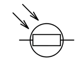
Fig 9 LDR
The basic principle of photoresistor is photoconductivity. This is an optical phenomenon where conductivity of material is increased when light is absorbed by the material. The photons when falls on the device valance band electrons are excited and jumps to the conduction band. These electrons have higher energy which is more than the band gap of the material. This helps them to jump from the valance band. Hence large number of charge carriers are generated when light strikes the material and current starts to flow.
IC 7805
This IC is a voltage regulator which maintains the output voltage at a constant value. The IC number defines the output voltage it provides. As this IC 7805 belongs to 78XX series so XX defines the output voltage it provides. 7805 provides +5V as output voltage. It has three pins input, ground and output pin.
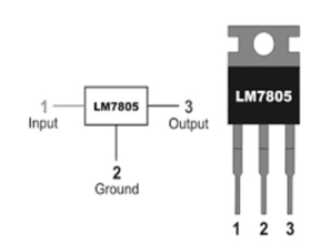
Fig 10 Pin Diagram of IC 7805
7805 IC Rating
Input voltage range 7V- 35V
Current rating Ic = 1A
Output voltage range VMax=5.2V, VMin=4.8V
The pin function and number are described below
PIN 1: It is the input pin through which positive unregulated voltage is fed.
PIN 2: It is ground pin which is neutral.
PIN 3: It is output pin and the output of the regulated voltage is taken through thus pin.
Heat Dissipation
The difference in the output and input voltage is dissipated in the form of heat. Depending upon the difference of these voltages heat dissipation can either be low or very high. If the difference is more than the heat dissipated can cause damage in the circuit elements. To overcome this suitable heat sink should be placed or the difference should be maintained to proper level. The formula for this is given as
Heat generated= (input voltage-5) x output voltage
Circuit for Regulated Power Supply
To form the circuit for regulated power, supply the IC 7805 is connected as shown below. The capacitor C1 acts as bypass capacitor and bypass small spikes in voltages to the ground. The other two capacitors C2 and C3 are known as filter capacitors C2 manages small changes in voltage given to the circuit. Whereas C3 manages slow changes in output voltage from regulator in the circuit. C4 is also used as by-pass capacitor which grounds the small spike in voltages to ground.
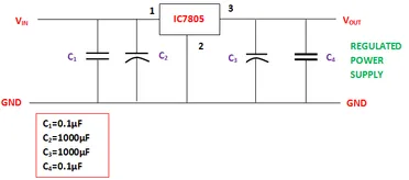
Fig 11 Regulated Power Supply Circuit
Applications
- As current Regulator
- Voltage Regulation
- Adjustable DC voltage Regulator
- In phone chargers, UPS power supply
- In portable CD players.
IC 7809
It is fixed voltage regulator IC. It is used in various applications. As already explained above this IC will provide voltage regulation of +9V as output. This IC can be used with some external components to obtain adjustable voltage.
The pin functions are similar to above.
PIN 1: It is the input pin through which positive unregulated voltage is fed.
PIN 2: It is ground pin which is neutral.
PIN 3: It is output pin and the output of the regulated voltage is taken through thus pin.
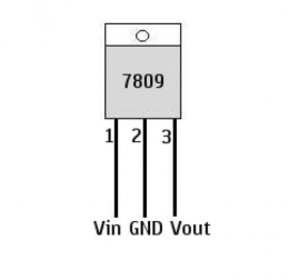
Fig 12 Pin diagram of IC 7809
IC 7812
It provides the output voltage of +12V as it belongs to the series 78XX. The ic 7812 is a positive voltage regulator which means that it generates the positive voltage with respect to the common ground.
In case if both the positive and negative voltage supply is needed in the same circuit. The voltage regulator ic 7812 is combined with its corresponding 79XX family IC that is 7912 IC.
The voltage regulator 7812 is available most commonly in TO-220 packageas well as TO-3, TO-92 and surface mount Packages.
The ic 7812 Voltage regulators do operate at their optimal capability, if the input voltage is at least 2.5 volt greater than the output voltage (i.e 14.5 V min.) and the current is 1 or 1.5 Amperes more. Though the voltage and current difference is different for other IC Packages.
PIN Configuration
PIN1 is the input pin.
PIN2 is the common pin between input and output.
PIN3 it is the output pin
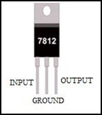
Fig 13 Pin diagram of IC 7812
IC 555
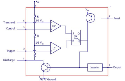
Fig 14 IC 555 Timer
For IC555 timer working as a flip flop or as a multi-vibrator, it has a particular set of configurations. Some of the major features include:
- It operates from a wide range of power ranging from +5 Volts to +18 Volts supply voltage.
- Sinking or sourcing 200 mA of load current.
- The external components should be selected properly so that the timing intervals can be made into several minutes along with the frequencies exceeding several hundred kilohertz.
- The output of a 555 timer can drive a transistor-transistor logic (TTL) due to its high current output.
- It has a temperature stability of 50 parts per million (ppm) per degree Celsius change in temperature which is equivalent to 0.005 %/ °C.
- The duty cycle of the timer is adjustable.
- Also, the maximum power dissipation per package is 600 mW and its trigger and reset inputs has logic compatibility.
Key takeaway
They can be used as frequency divider, PWM, SR F/F, missing pulse detection etc.
Measuring Instruments like CRO
They are generally used in laboratories. They are used to measure various waveforms. This device is very fast in plotting two dimensional characteristics. In this instrument a beam of electrons strikes a luminous screen and produce luminous spots. These spots move according to the variation of input variable.
Construction of CRO
The CRO consists of
1) Cathode ray tube: It is a vacuum tube which converts electrical signal into the visual signal. It has an electron gun and electrostatic deflection plates. A focused beam of electrons of high frequency is produced by electron gun. The electron beam is moved left to right by horizontal beam and vertical deflection plate moves the beam up and down.
2) Electronic gun assembly: This gun emits electron and form them into beam. It has heater, cathode, a grid, a focusing anode and an accelerating anode. There is a layer of barium and strontium to provide high emission of electrons at moderate temperature. The electron passes to control grid from the cathode grid. The CRO uses an electrostatic focusing tube.
3) Deflecting plate: The electron beam passes through two pair of deflecting plate after leaving the electron gun. The vertical deflecting plate produces vertical deflection and horizontal deflecting plate produces horizontal deflection.
4) Fluorescent Screen for CRT: The front of CRT is called face plate. It formed by shaping molten glass. The inner surface is coated with phosphor crystal which converts electric energy to light energy. When electron beam strikes the surface their energy level is raised and hence light is emitted.
5) Glass Envelop: It is conical shaped structure. There is aquadag coating between screen and inner surface of CRT. This surface is electrically connected to accelerating anode helping the electron beam to focus.
Working
The CRO figure is shown below. The electron is injected through control grid. This control grid has to control the light intensity of electron. The intensity of light depends on the negative potential of control grid. If the negative potential is low bright spot is produced and vice versa.
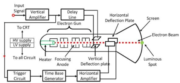
Fig 15 CRO
The electron beam further passes through focusing and accelerating anodes. These anodes being at high positive potential converge the beam to a point on screen. The beam than comes under the deflecting plates. The beam produces a spot when deflecting plate is at zero potential. The electron beam focuses upward when voltage is applied to vertical plate, and it is deflected horizontally when the voltage is applied to horizontal plate.
Measurements using CRO – Voltage, Current, Frequency, Time and Phase angle
Measurements of Voltage and Current
For measuring direct voltage, the spot is focused on the centre without applying any voltage to the deflection plate. The deflection of the spot is noticed on screen after applying direct voltage in between the deflection plates. The direct voltage is equal to the product of magnitude of deflection and the deflection factor. For measuring AC voltage, it is applied between pair of deflection plate and the straight line is measured.
The current to be measured is passed through a known non-inductive resistance and the voltage across it is measured. The current can be determined by dividing the voltage drop by non-inductive resistance.
Measurement of Frequency
The pattern on CRO screen is called as Lissajous pattern. These patterns are stationary on screen. There are two types of Lissajous patterns open pattern with free ends and closed pattern with no free ends.
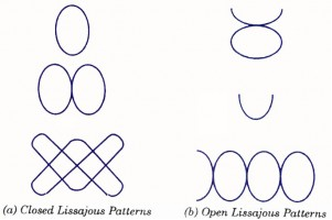
In these patterns the ratio of frequency of vertical signal to frequency of horizontal signal is equal to ratio of y-peaks to X-peaks. Thus, by counting the positive Y-peaks and X-peaks on a Lissajous pattern, ratio of frequencies of two voltage signals can be determined.
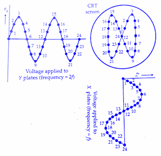
When a sine wave is applied to both plates but the frequency of wave at Y plate is twice to that of the X plate. Then the output will have a pattern of 8 with two loops because both the waves start at same instance. But when same frequency wave does not start at same instance the patterns obtained are below
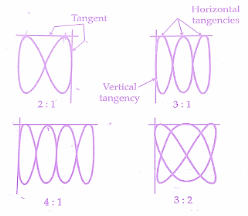
The ratio of frequency will be
 =
= 
The above equation will not hold for Lissajous pattern with free ends. For this case the equation becomes
 =
= 
Measurement of Time
The voltage signal as a function of time is seen on CRO. The number of divisions that are in one period of cycle can be varied by time/division knob. The time period is T=j nv
j: time/division
Nv: number of partitions of one cycle in horizontal way
Measurement of Phase
The Lissajous pattern helps us to determine the phase of the signal applied. When a sinusoidal voltage of same frequency is applied to both the plates then a straight line appears on screen. This pattern shows that there is no phase shift as well.
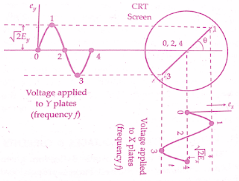
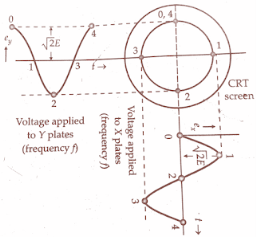
Now when two voltages of same frequency but 90o phase shift is applied then then a circle is seen on the CRO screen.
Now the other case possible will be two same voltages with same frequency but phase shift other than 90o is applied. The pattern observed on screen is an ellipse. This patter (ellipse) is also obtained when unequal voltages of same frequency are applied.
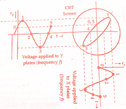
The ellipse actually provides a measurement of phase difference between two voltages.
Sinφ =  =
= 
When the major axis in 1st and 3rd quadrant then the phase difference is either 00o-90o or it can be 270o-360o.
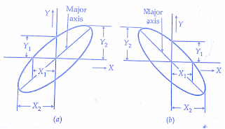
When the major axis is in 2nd and 4th quadrant (slope negative) then the phase difference is either 90o-180o or 180o-270o
Power Supply
It is an electronic instrument that supplies electric energy to the load. Its main task is to convert one form of electric energy to other. The regulated power supply means it supplies power to variety of output voltages for bench testing of electronic circuits, with variation of output voltages. Usually DC power source is used by electronic devices for operation. The regulated power supply consists of ordinary power supply and voltage regulating device. The voltage regulating device takes input from the ordinary power supply producing final output.
Function Generator
The function generator is an instrument which generates different types of wave form. The most required common wave forms are sine wave, saw tooth wave, triangle wave, square wave and these various outputs of the generator are available simultaneously. The purpose of providing simultaneously waves is fulfilled by the function generator. In function generator the o/p waveform can be generated at a desired freqn in range from few hertz to several kilohertz. In the function generator the freqn is controlled which drives the integrator. The freqn controlled vtg is used to regulate two current source namely upper current source and lower current source. The upper current source supplies constant current to an integrator. The o/p vtg of integrator then increases linearly with time. If the current charging the capacitor increases or decreases the slope of o/p vtg increases or decreases respectively. Hence this controls freqn.
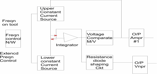
Fig 16 Block diagram of function generator
- The voltage comparator multi vibrator circuit changes the state of the n/w when the o/p vtg of integrator equals the maximum predetermined upper level.
- Because of this change in state the upper current source is removes and the lower current source is switched on
- This lower current source supplies opposite current to the integrator or ckt. The o/p of integrator decreases linearly with time when this o/p vtg equals maximum predetermine upper level on –ve side the comparator multi vibrator again changes the condition of the n/w by switching off the lower current source and switching on the upper current source
- The o/p vtg of the integrator has triangular wave form
- The freqn of this triangular wave form is determined by the upper current source and lower current source
- To get square wave the o/p of the integrator is passed through comparator.
- The vtg comparator delivers square wave o/p vtg of same freqn as that of i/p triangular wave form
- The sine wave is derived from triangular wave. The triangular wave is synthesised in to sine wave using diode resistance n/w in this shaper ckt , the slope of triangular wave is changed as it amplitude changes. This result in a sine wave with less than 1% distortion
- The two o/p amplifiers provide two simultaneous individually selected o/p of any of the wave form functions.
Application:
- It is used to generate different types of waves form simultaneous such as sine wave, square wave, triangular wave & saw tooth wave at a desired frequency from few hertz to several kilohertz.
- It is used to test bandwidth of audio frequency amplifier using square wave testing method
- It can be used in trouble shooting of various Analog as well as digital instruments.
- It is most extensively used as signal source for radio receiver alignment procedure.
Multi-meters
- A Multi meter the most common measuring instrument. The name comes from multiple meters. There are two common types of Multi meter.
- The multi-meter (DMMs) are the most common Measurement readings are displayed as numerical values on the LCD display. The display also alerts you to any pertinent symbols and warning.
- Digital meters on the other hand offer high accuracy have a high i/p impedance and are smaller in site.
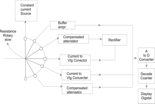
Fig 17 Block Diagram of Multi-meter
An instrument which is capable of measuring a.c. And d.c voltages a.c and d.c. Current and resistances over several range is called digital multimeter. The various measurement possible by DMM are resistance a.c voltage and current d.c voltage and current.The selection of the parameter is possible with the help of rotary switch connected to i/p probes of DMM.
- Resistance Measurement: The rotary switch is in position 1 and resistance is connected to input probes. The constant current source Drives a current through unknown resistance. This produces Voltage across resistance which is directly proportional to the resistance. It is given to the buffer amplify and then to analog to digital converter. The ADC converts it to equivalent digital signal and it is displayed with the help of digital display a.c voltage measurement : The rotary switch is in position 2 and i/p a.c voltage is applied to probes if it is above the selected range it is attenuated with the help of compensated attenuator It is rectified to produce proportional d.c voltage then it is given to ADC which display it in volts
- A.c current measurement: the rotary switch is in position 3 and unknown current is applied across i/p probes it is converted to proportional voltage using current to voltage convertors
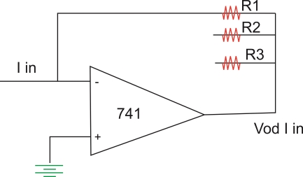
This I V converter is op-amp circuit as shown above. The op-amp/p current is zero hence I in flows through R1 and drop across R1osVo hence vtg o/p  the resistance R1 R2 and R3 are used for the proper range selection. This vtg is rectified and then given to ADC which displays the current in amperes.
3. D.c current measurement: The rotary switch is in position 4 and unknown d.c current is applied across i/p probes this vtg is given to ADC without rectification as this is proportional to d.c current ADC display it in amperes on digital display.
4. D.C voltage measurement: The rotary switch is in position 5 and unknown vtg is applied across i/p probes it is attenuated and directly given to ADC display it in volts.
Specifications of Digital Multi-meter:
- D.C Voltage : this includes various d.c vtg ranges available along with the resolution and accuracy
- A.c Voltage : this includes various a.c vtg ranges available along with the resolution and accuracy.
- A.C current : this includes various a.c current ranges available along with the resolution and accuracy.
- Resistance : this includes the available resistance range typical six range are available from 200Ω to 20 MΩ the accuracy is
 0.1% of reading + two digits + 0.002Ω on the lowest range.
 - Input Impedance : The i/p Impedance is about 10 MΩ on all the range
- Normal mode noise rejection : this indicates the ability of the meter
It is greater than 60 dB at 50 HZ while the common mode noise rejection is greater than 90 dB at 50 HZ and greater than 120 dB at d.c
7. Overload protection: The overload protection of 1000 V d.c and 75 0ɤ.m.s. a.c is provided.
8. Diode test: The vtg drop across the diode can be measured for which 1 mA + 10% of constant current source is used.
9. Conductance: It can display Conductance in siemens
10. Relative Reference: when RF1 button is pressed the displayed reading is stored as a reference and then subtracted from the subsequent readings to indicate only amount of deviation from the reference.
11. Frequency: The frequency ranges is 200HZ to 200 kHZ auto selection.
References:
1. Integrated Devices & Circuits by Millman & Halkias, TMH Publications.
2. Electronics Devices and Circuit Theory by R. Boylestad & L. Nashelsky, Pearson Publication
3. Electronic Communication System by G. Kennedy, TMH Publications.
4. Basic Electronics by Sanjeev Kumar & Vandana Sachdeva, Paragaon International Publication