Unit - 3
Transistors
Bipolar junction transistor or BJT is simply known as Transistor. A transistor consists of two pn junctions formed by sandwiching either p-type or n-type semiconductor between a pair of opposite types.
The prefix 'trans' means the signal transfer property of the device while 'istor ' classifies it as a solid element in the same general family with resistors. Accordingly, there are two types of transistors
- n-p-n transistor
- p-n-p transistor
An n-p-n transistor is composed of two n-type semiconductors separated by a thin section of p-type as shown in Figure 1 (i).
However, a p-n-p transistor is formed by two p-sections separated by a thin section of n-type as shown in Figure 1(ii).

Figure1: (i) n-p-n transistor (ii) p-n-p transistor
In each type of transistor, the following points may be noted:
(i) Transistor may be regarded as a combination of two diodes connected back to back.
(ii) There are three terminals, one taken from each type of semiconductor.
(iii) The middle section is a very thin layer. The thin layer plays an important role in the function of a transistor.
A transistor has two pn junctions. One junction is forward biased and the other is reverse biased. The forward biased junction has a low resistance path whereas a reverse biased junction has a high resistance path. The weak signal is introduced in the low resistance circuit and output is taken from the high resistance circuit. Therefore, a transistor transfers a signal from a low resistance to high resistance.
A transistor (pnp or npn) has three sections of doped semiconductors. The section on one side is the emitter and the section on the opposite side is the collector. The middle section is called the base and forms two junctions between the emitter and collector.
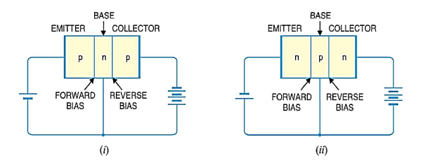
Figure 2: (i) p-n-p transistor (ii) n-p-n transistor
Emitter: The section on one side that supplies charge carriers (electrons or holes) is called the emitter. The emitter is always forward biased w.r.t. Base so that it can supply a large number of majority carriers. In Figure 2 (i), the emitter (p-type) of pnp transistor is forward biased and supplies hole charges to its junction with the base. Similarly, in Figure 2 (ii), the emitter (n-type) of npn transistor has a forward bias and supplies free electrons to its junction with the base.
Collector: The section on the other side that collects the charges is called the collector. The collector is always reverse biased. Its function is to remove charges from its junction with the base. In Figure 2 (i), the collector (p-type) of pnp transistor has a reverse bias and receives hole charges that flow in the output circuit. Similarly, In Figure 2 (ii), the collector (n-type) of npn transistor has reverse bias and receives electrons.
Base: The middle section which forms two pn junctions between the emitter and collector is called the base. The base emitter junction is forward biased allowing low resistance for the emitter circuit. The base-collector junction is reverse biased and provides high resistance in the collector circuit.
Before studying action of transistor, some important facts about transistor should be keep in mind.
- The transistor has two pn junctions i.e. it is like two diodes. The junction between emitter and base may be called emitter-base diode or simply the emitter diode. The junction between the base and collector may be called collector-base diode or simply collector diode.
- The emitter diode is always forward biased whereas collector diode is always reverse biased.
- Three regions of transistor are emitter, base and collector. The base is much thin as compared to emitter while "collector is wider than both. To keep it simple it is assumed emitter and collector is considered to be of same size.
- The emitter is heavily doped so that it can inject a large number of charge carriers (electrons or holes) into the base. The base is lightly doped and very thin it passes most of the emitter injected charge carriers to the collector. The collector is moderately doped.
- The resistance of emitter diode (forward biased) is very small as compared to collector diode (reverse biased). Therefore, forward bias applied to the emitter diode is generally very small whereas reverse bias on the collector diode is much higher.
Working of Transistor
(i) Working of npn transistor: As discussed in the npn transistor emitter-base junction is forward biased to emitter-base junction and collector-base junction is reverse biased. The forward bias causes the electrons in the n-type emitter to flow towards the base. This constitutes the emitter current Ie.
Ie = Ib + Ic
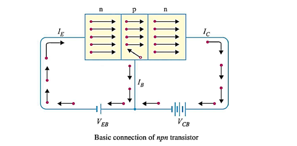
Figure 3: n-p-n transistor
As these electrons flow through the p-type base, they tend to combine with holes. As the base is lightly doped and very thin, therefore, only a few electrons (less than 5%) combine with holes to constitute base current Ib. The remainder i.e. more than 95% cross over into the collector region to constitute collector current Ic In this way, almost the entire emitter current flows in the collector circuit. It is clear that emitter current is the sum of collector and base currents i.e.
(ii) Working of pnp transistor: In the pnp transistor emitter-base junction is forward biased to emitter-base junction and collector-base junction is reverse biased. The forward bias causes the holes in the p-type emitter to flow towards the base. This constitutes the emitter current Ie. As these holes cross into n-type base, they tend to combine with the electrons. As the base is lightly doped and very thin, therefore, only a few holes (less than 5%) combine with the electrons.
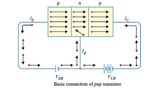
Figure 4: p-n-p transistor
The remainder (more than 95%) cross into the collector region to constitute collector current Ic. In this way, almost the entire emitter current flows in the collector circuit. It may be noted that current conduction within pnp transistor is by holes. However, in the external connecting wires the current is still by electrons.
Thus the input circuit (i.e. emitter-base junction) has low resistance because of forward bias whereas output circuit (i.e. collector base junction) has high resistance due to reverse bias. As we have seen, the input emitter current almost entirely flows in the collector circuit. Therefore a transistor transfers the input signal current from a low resistance circuit to a high-resistance circuit.
Transistor’s Configuration:-
1) Common Base configuration(C.B)
2) Common emitter Configuration(C.E)
3) Common Collector Configuration(C.C)
COMMON BASE CONFIGURATION
The notation and symbols of pnp and npn transistors are given below:
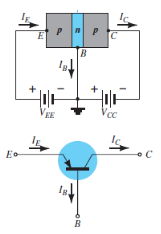
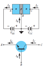
Figure 5: PNP CB and NPN CB (Ref. 2)
Here the base is common to both the input and output sides of the configuration.
The flow of holes will govern the direction of current.
Hence, Ic = Ib + Ie
Where Ic, Ib, Ie are the collector, base and emitter currents respectively.
The graphical symbol of the PNP common base configuration is
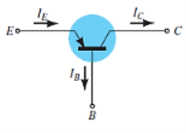
Figure 6: PNP common base(Ref. 2)
The arrow in the above symbol shows the direction of emitter current in the device.
Now, to study the behavior of the device we require two characteristics:
Input Characteristic Curve
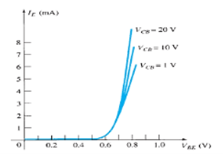
Figure 7: Input Characteristic Curve (Ref. 2)
- It is the relation between the input current IE to the input voltage VBE for various levels of output voltage VCB.
- It is also known as driving point characteristics.
Output Characteristic Curve
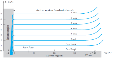
Figure 8: Output Characteristic Curve (Ref. 2)
- It is the relation between the output current IC to the output voltage VCB for various levels of input current IE.
- It is also known as collector set of characteristics.
- It has three basic regions:
- Active Region
Here, base-emitter junction is forward biased and collector-base junction is reverse biased.
As input current IE increases above zero, output current IC increases to a magnitude equal to IE as determined by the basic transistor current relationship.
So the first approximation determined by the curve is
IC ≈ IE
2. Cut-off Region
It is defined as the region where the collector current IC is equal to 0A.
Here, the base-emitter junction and the collector-base junction both are in reverse bias.
3. Saturation Region
It is the region that lies towards the left of VCB = 0V.
Here, the base-emitter junction and the collector-base junction both are in forward bias.
COMMON EMITTER CONFIGURATION
The notation and symbols of npn and pnp transistors are given below:
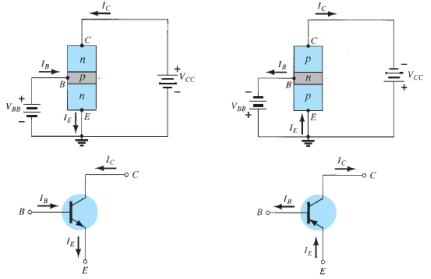
Figure 9: NPN CE and PNP CE (Ref. 2)
In the above figure all the currents are shown in their actual conventional directions.
The current relation developed earlier is still applicable,
IE = IB + IC
Where IE , IB , IC are the collector, base and emitter currents respectively.
The graphical symbol of the PNP common emitter configuration is
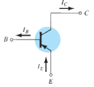
Figure 10: PNP common emitter (Ref. 2)
Now, to study the behavior of the device we require two characteristics:
Input Characteristic Curve
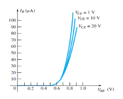
Figure 11: Input Characteristic Curve (Ref. 2)
It is the graph between the input current IB to the input voltage VBE for a range of values of output voltage VCE.
Note that the magnitude IB of is in micro amperes and that of IC is in milli amperes.
Output Characteristic Curve
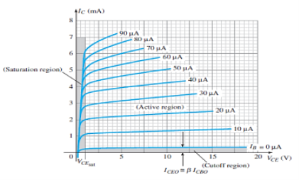
Figure 12: Output Characteristic Curve (Ref. 2)
It is the graph between the output current IC to the output voltage VCE for a range of values of input current IB.
It has three basic regions:
Active Region
- Here, the base-emitter junction is forward biased and collector base junction is reverse biased.
- These are the same conditions that existed in the active region of the common base configuration.
- This can be employed for voltage, current or power amplification.
Cut-off Region
- Here IC is not equal to zero when IB is zero.
- For linear amplification purposes, it is defined as IC = ICEO .
- The region below IB = 0µA is to be avoided for undistorted output signal.
- When the transistor is used as a switch, the condition should be ideally IC = 0mA for a chosen VCE voltage.
Saturation Region
- It is the region that lies towards the left of VCE = 0V.
COMMON COLLECTOR CONFIGURATION
The notation and symbols of npn and pnp transistors are given below:
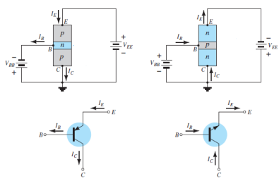
Figure 13: NPN CC and PNP CC (Ref. 2)
In the above figure all the currents are shown in their actual conventional directions.
It is used for impedence matching purposes as it has high input impedence and low output impedence.
It can be designed using common emitter characteristics.
The output characteristics of common collector is same as that of common emitter configuration for all practical purposes.
The output characteristics are a plot between IE versus VCE for all values of IB.
The input current of common collector is same as that of common emitter configuration.
Here the region of operation will ensure that maximum ratings are not being exceeded and output ratings have minimum distortion.
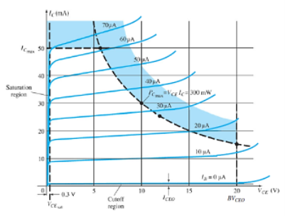
Figure 14: Output Characteristic Curve (Ref. 2)
The characteristics specifying the minimum VCE that can be applied without entering the non-linear region is saturation region.
The maximum power dissipation is given by,
P = VCE . IC
Key Takeaways
- A transistor consists of two pn junctions formed by sandwiching either p-type or n-type semiconductor between a pair of opposite types.
- There are two types of transistors n-p-n transistor and p-n-p transistor.
- The emitter diode is always forward biased whereas collector diode is always reverse biased.
- Three regions of transistor are emitter, base and collector. The base is much thin as compared to emitter while "collector is wider than both. To keep it simple it is assumed emitter and collector is considered to be of same size.
- The emitter is heavily doped so that it can inject a large number of charge carriers (electrons or holes) into the base. The base is lightly doped and very thin it passes most of the emitter injected charge carriers to the collector. The collector is moderately doped.
- Transistor’s Configuration:-Common Base configuration(C.B), Common emitter Configuration(C.E), Common Collector Configuration(C.C)
Comparison of all configuration
Sr.no | Parameter | CB | CE | CC |
1 | Common terminal between I/p & o/p | Base | Emitter | Collector |
2 | Input Current | IE | IB | IB |
3 | Output Current | IC | IC | IE |
4 | Current Gain |   |   | ɤ=   |
5 | Input Voltage. | VEB | VBE | VBC |
6 | Output Voltage. | VCB | VCE | VCC |
Comparison of all Modes
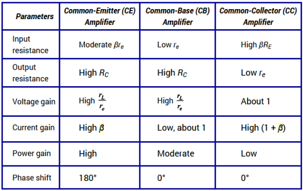
BJT as a switch
Suppose we had a lamp that we wanted to turn on and off with a switch. Such a circuit would be extremely simple, as in the figure below.

a- mechanical switch
b- NPN transistor switch
c- PNP transistor switch
Figure 15. Transistor as switch
Suppose we insert a transistor in place of the switch to show how it can control the flow of electrons through the lamp. Remember that the controlled current through a transistor must go between collector and emitter.

Figure 16. Transistor: a) cut-off lamp b) saturated, lamp on.
The choice between NPN and PNP is really arbitrary. All that matters is that the proper current directions are maintained for the sake of correct junction biasing.
In the above figures, the base of either BJT is not connected to a suitable voltage, and no current is flowing through the base. Consequently, the transistor cannot turn on. Therefore, connect a switch between the base and collector wires of the transistor as in figure.
If the switch is open as in figure (a), the base wire of the transistor will be left “floating” and there will be no current through it. In this state, the transistor is said to be cut-off.
If the switch is closed as in figure (b), current will be able to flow from the base to the emitter of the transistor through the switch. This base current will enable a much larger current flow from the collector to the emitter, thus lighting up the lamp. In this state of maximum circuit current, the transistor is said to be saturated.
BJT as an Amplifier
Transistor raises the strength of a weak signal and hence acts an amplifier. The transistor amplifier circuit is shown in the figure below.
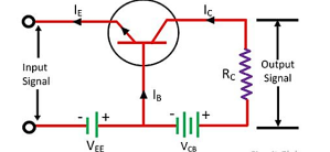
Figure 17. Transistor as an Amplifier
The transistor has three terminals namely emitter, base and collector. The emitter and base of the transistor are connected in forward biased and the collector base region is in reverse bias. The forward bias means the P-region of the transistor is connected to the positive terminal of the supply and the negative region is connected to the N-terminal and in reverse bias just opposite of it has occurred.
Vee is applied to the input circuit along with the input signal to achieve the amplification. The DC voltage VEE keeps the emitter-base junction under the forward biased condition regardless of the polarity of the input signal and is known as bias voltage.
When a weak signal is applied to the input, a small change in signal voltage causes a change in emitter current this change is almost the same in collector current because of the transmitter action.
In the collector circuit, a load resistor RC of high value is connected. When collector current flows through such a high resistance, it produces a large voltage drop across it. Thus, a weak signal (0.1V) applied to the input circuit appears in the amplified form (10V) in the collector circuit.
Input Resistance
When the input circuit is forward biased, the input resistance will be low. The input resistance is the opposition offered by the base-emitter junction to the signal flow.
Hence, it is the ratio of small change in base-emitter voltage (ΔVBE) to the resulting change in base current (ΔIB) at constant collector-emitter voltage.
Input resistance, Ri=ΔVBE/ΔIb
Where Ri = input resistance, VBE = base-emitter voltage, and IB = base current.
Output Resistance
The output resistance of a transistor amplifier is very high. The collector current changes very slightly with the change in collector-emitter voltage.
The ratio of change in collector-emitter voltage (ΔVCE) to the resulting change in collector current (ΔIC) at constant base current.
Output resistance = Ro=ΔVCE/ΔIC
Where Ro = Output resistance, VCE = Collector-emitter voltage, and IC = Collector-emitter voltage.
Current gain
It is the ratio of change in collector current (ΔIC) to the change in base current (ΔIB).
Current gain, β=ΔIC/ ΔIB
Voltage Gain
It is the ratio of change in output voltage (ΔVCE) to the change in input voltage (ΔVBE).
Voltage gain, AV=ΔVCE/ΔVBE

Power Gain
It is the ratio of output signal power to the input signal power.
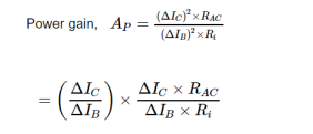
= current gain x voltage gain
Construction
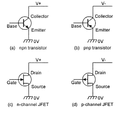
- An FET is a three-terminal amplifying device.
- Its terminals are source, gate, and drain, which acts respectively like emitter, base, and collector of a normal transistor.
- There are two distinct families of FETs.
- The first is known as ‘junction-gate’ types of FETs or JUGFET or JFET.
- The second family is called ‘insulated-gate’ FETs or Metal Oxide Semiconductor FETs or MOSFET.
- ‘N-channel’ and ‘p-channel’ are the two versions of both types of FET.
Working
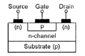
- N-channel FET consists of n-type semiconductor material with a drain terminal and a source terminal at opposite ends.
- A p-type gate is joined in the middle section of the n-type bar, thus forming a p-n junction.
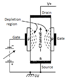
- The drain terminal is connected to a positive supply and the gate is biased at a value that is negative (or equal) to the source voltage, thus reverse-biasing the JFET’s internal p-n junction, and accounting for its very high input impedance.
- When gate = 0V, a current flow from drain to source via a conductive ‘channel’ and the n-type bar is formed.
- When gate = negative , a high resistance region is formed within the junction, thus reduces the magnitude of the drain-to-source current and width of the n-type conduction channel.
- Thus, the basic JFET passes maximum current when its gate bias is zero, and its current is reduced or ‘depleted’ when the gate bias is increased. It is thus known as a ‘depletion-type’ n-channel JFET.
JFET parameters
1. Gate Cut Off Voltage
At a fixed drain voltage, the drain current (ID) of a JFET depends on the gate to source voltage (VGS). If the gate to source voltage decreases in n channel JFET, the drain current also gets decreased accordingly.
The relation between gate to source voltage and drain current is given by
2. Shorted Gate Drain Current
When (VGS = 0) and positive drain to source voltage (VDS) is being increased slowly, the drain current gets increased linearly. But after pinch-off voltage (Vp), the drain current increases and gets a constant value. This is the maximum drain current that flows through the channel and is called shorted gated drain current and denoted by IDSS.
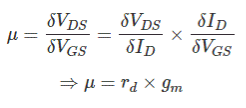
3. Transconductance
Transconductance is defined as the ratio of change in drain current (δID) to change in the gate to source voltage (δVGS) with a constant drain to source voltage (VDS = Constant).
4. Dynamic Output Resistance
It is the ratio of change of drain to source voltage (δVDS) to the change of drain current (δID) keeping a constant gate to source voltage (VGS = Constant). The ratio is denoted as rd.

5. Amplification Factor
It is defined as the ratio of change of drain voltage (δVDS) to change of gate voltage (δVGS) at a constant drain current (ID = Constant).
There is a relation between transconductance (gm) and dynamic output resistance (rd) and is given as.
JFET characteristics
There are two types of static characteristics viz
(1) Output or drain characteristic
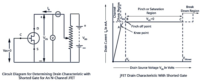
(a) Drain Characteristic with Shorted-Gate
- The curve drawn between drain current Ip and drain to source voltage VDS with gate to source voltage VGS as the parameter is called the drain or output characteristic.
- When Vns = zero, there is no potential at the drain, therefore no current flows.
- Hence drain current ID = 0.
- For small voltage Vna, the N-type bar acts as a semiconductor resistor, and the drain current increases linearly with the increase in Vds.
- The region present to the left of the knee point is called the channel ohmic region, as in this region the FET behaves like an ordinary resistor.
(b)Drain Characteristics With External Bias
Here, the circuit diagram determines the drain characteristics with different values of external bias and a family of drain characteristics for different values of gate-source voltage VGS.
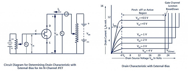
As the negative gate bias voltage increases:
(1) The maximum saturation drain current becomes smaller because the conducting channel becomes narrower.
(2) Pinch-off voltage reaches at a lower value when VGS = 0.
(3) The ohmic region portion decreases.
(4) The value of drain to source voltage VDS for the avalanche breakdown of the gate junction is reduced.
Hence, in the pinch-off or active region it is necessary to satisfy the following conditions:
VP < VDS < VDS (max)
VGS (OFF)< VGS < 0
0 < ID < IDSS
(2) Transfer characteristic.
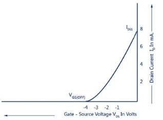
It is determined by experimentally keeping drain to source voltage, VDS constant and determining drain current, ID for various values of gate-source voltage, VGS. The curve is plotted between gate to source voltage, VGS and drain current, ID. It is observed that
(i) ID decreases with the increase in negative gate to source voltage
(ii) ID = IDSS when VGS = 0
(iii) ID = 0 when VGS = VD
Key takeaway
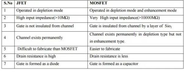
MOSFETs are three terminal devices with a Gate, Drain and Source and both P-channel (PMOS) and N-channel (NMOS) MOSFETs are available. The main difference this time is that MOSFETs are available in two basic forms:
- Depletion Type – the transistor requires the Gate-Source voltage, ( VGS ) to switch the device “OFF”. The depletion mode MOSFET is equivalent to a “Normally Closed” switch.
- Enhancement Type – the transistor requires a Gate-Source voltage, ( VGS ) to switch the device “ON”. The enhancement mode MOSFET is equivalent to a “Normally Open” switch.
The symbols and basic construction for both configurations of MOSFETs are shown below.
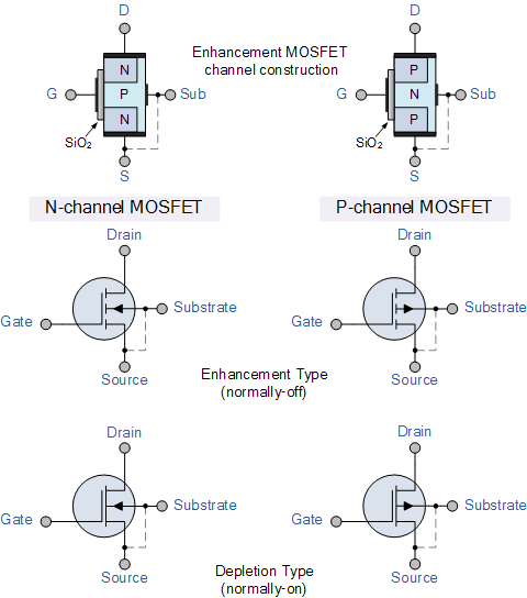
The four MOSFET symbols above show an additional terminal called the substrate and is not normally used as either an input or an output connection but instead it is used for grounding the substrate. It connects to the main semiconductive channel through a diode junction to the body or metal tab of the MOSFET.
The line in the MOSFET symbol between the drain (D) and source (S) connections represents the transistors semiconductive channel. If this channel line is a solid unbroken line then it represents a “Depletion” (normally-ON) type MOSFET as drain current can flow with zero gate biasing potential.
If the channel line is shown as a dotted or broken line, then it represents an “Enhancement” (normally-OFF) type MOSFET as zero drain current flows with zero gate potential. The direction of the arrow pointing to this channel line indicates whether the conductive channel is a P-type or an N-type semiconductor device.
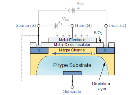
The construction of the Metal Oxide Semiconductor FET is different to that of the Junction FET.
Both the Depletion and Enhancement type MOSFETs use an electrical field produced by a gate voltage to alter the flow of charge carriers, electrons for n-channel or holes for P-channel, through the semi-conductive drain-source channel.
The gate electrode is placed on top of a very thin insulating layer and there are a pair of small n-type regions just under the drain and source electrodes.
With the insulated gate MOSFET device no such limitations apply so it is possible to bias the gate of a MOSFET in either polarity, positive (+ve) or negative (-ve).
This makes the MOSFET device especially valuable as electronic switches or to make logic gates because with no bias they are normally non-conducting and this high gate input resistance means that very little or no control current is needed as MOSFETs are voltage controlled devices.
Both the p-channel and the n-channel MOSFETs are available in two basic forms, the Enhancement type and the Depletion type.
MOSFET is another type of field effect transistor. The MOSFET has become one of the most important devices used in design and construction computers
MOSFET [metal oxide semiconductor field effect transistor]
Type of MOSFET
- Depletion type MOSFET
- Enhancement type MOSFET
- Power MOSFET
Enhancement type MOSFET: classified in to two type n. Channel or p. Channel E MOSFET
A) N-channel E MOSFET
B) P-channel E MOSFET
N-channel E MOSFET
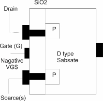
Figure 18: N-channel E MOSFET
- A slab of P-type semiconductor is used as substrate. The substrate is sometimes connected to the source otherwise it is brought out as the fourth terminal.
- The drain and source terminal are connected to the n-type doped regions through the metallic contacts.
- The insulating sio2 layer is still present which isolates gate terminal from the substrate.
Effect of the insulting sio2 layer:
Due to the presence of the sio2 layer between gate terminal and n-type channel the i/p impedance of MOSFET is very high this is a desirable fracture of a MOSFET. Due to high i/p impedance the gate current IG= 0 for the d.c operating conditions.
Operation: the operation can be explained with two different operating
- Operation with VGS = 0
- Operation when VGS is +ve
1) Operating with VGS = 0 Volt
If VGS = 0 and a positive voltage is applied between its drain and source, then due to the absence of the n-type channel a zero drain current will result.
2) Operation when Vgs Positive:
The positive potential at the gate terminal will repel the holes present in the p-type substrate.
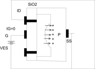
Figure 19: Operation on N-channel E MOSFET
Formation of induced channel in n-channel enhancement MOSFET
This creates a depletion region near the sio2 insulating layer. But the minority carriers ie the electrons in the p-type substrate will be attracted towards the gate terminal and gather near the surface of sio2 as shown above
As we increase the positive VGS the number of e- gathering near the sio2 layer increases to such an extent that it creates an induced n-channel which connects the n-type doped regions.
The drain current then starts flowing through this induced channel. The value of VGS at which this conduction begins is called as the threshold Vtg. & is indicated.
V-I Characteristics
Characteristics of n-channel enhancement type MOSFET:
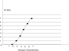
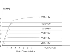
Transfer characteristics drain characteristics
Figure 20: Characteristics of n-channel enhancement type MOSFET
P-channel enhancement type MOSFETS:
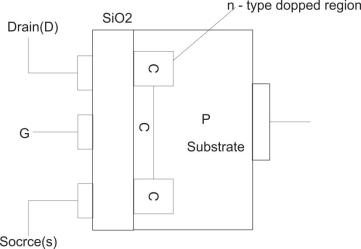
Figure 21: P-channel enhancement type MOSFETS
The construction of p-channel EMOSFET is exactly opposite to that of a n-channel EMOSFET.
Characteristics:
Drain Characteristics of transfer Characteristics of p-channel E MOSFET
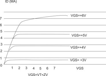
Figure 22: Characteristics of p-channel enhancement type MOSFET
Regions Of Operation, MOSFET As Switch & Amplifier
Operation: the operation can be explained with two different operating
Operation with VGS = 0
Operation when VGS is +ve
Operating with VGS = 0 Volt
If VGS = 0 and a positive voltage is applied between its drain and source, then due to the absence of the n-type channel a zero drain current will result.
Operation when Vgs Positive:
The positive potential at the gate terminal will repel the holes present in the p-type substrate.
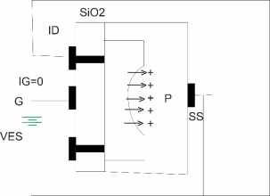
Figure 23: Formation of induced channel in n-channel enhancement MOSFET
Formation of induced channel in n-channel enhancement MOSFET
- This creates a depletion region near the sio2 insulating layer. But the minority carriers ie the electrons in the p-type substrate will be attracted towards the gate terminal and gather near the surface of sio2 as shown above
- As we increase the positive VGS the number of e- gathering near the sio2 layer increases to such an extent that it creates an induced n-channel which connects the n-type doped regions.
- The drain current then starts flowing through this induced channel. The value of VGS at which this conduction begins is called as the threshold Vtg. & is indicated
Effect of increase in the drain to source Vtg.:
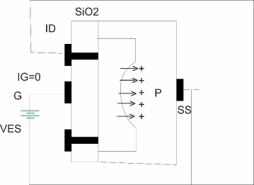
Figure 24: Effect of increase in the drain to source Vtg:
Effect of changes in VDS at fixed VGS on the channel width:
- The positive gate to source voltage VDS is kept constant and the drain to source voltage VGS is increased gradually.
- Due to this the gate terminal becomes less and less positive with respect to the drain so less number of electron are attracted towards gate terminal & the induced channel becomes narrow.
- Eventually the channel width will be reduced to a point of pinch off and the saturation condition will be established which is same as that in a JFET
- That means any further increase in VDS at the fixed value of VGS will not affect the saturation level of ID unless breakdown condition are encountered.
Symbols:
1) N-channel EMOSFET
2) P-channel EMOSFEJ
BJT is a bipolar device [minority & majority carriers both contributes to the current flow]
E MOSFET is a unipolar device ie current flows only due to the majority carriers
BJT thermal runaway can damage BJT thermal runway does not take place.
BJT low i/p impedance, E MOSFET High i/p impedance
- Voltage ampɤ :
- Current and vtg gain
Current gain AI is defined as the ratio of o/p current

Vtg gain is given by
Av = Vo/V


In this expression if Ro is very small as compared to RL then Av A
A
Thus we can say that the overall gain of the ampere Av will approach its open circuit value A if Ro << RL
Problem: An amplifier has a signal i/p Vtg. Vi of 0.25v and draws 1mA from the source. The amɤ delivers & v to a load at 10 mA. Determine the current Vtg and power gains. Also find the i/p resistance of this ampɤ what must be the open ckt. Vtg of the source Vs to provide an ampɤ i/p VtgVi of 0.25 v when the internal resistance of the source is 50 Ω?
Given Vi = 0.25v, Ii = 1 Ma, Vo = 8 v, Io = 10 mA, Rs = 50 Ω.
Solution:
Vtg gain Av = 
Current gain =
= 
Power gain AP = Av  = 32
= 32 
Input resistance Ri =  = 250
= 250
Open circuit Vtg of Vs
Vi = 
Vs = 
Vs = 
Vs = 0.3v
MOSFET as switch:
- MOSFET can act as a switch jest like a transistor a typical switching Ckt using N-channel EMOSFET shown below
- A positive going i/p pulse (high i/p) turns on the EMOSFET. Maxm drain current flows and the o/p Vtg drops from +VDD to RD ID (on). So the EMOSFET acts as closed switch.
- Similarly when the i/p is low (zero) no drain current and hence the o/p is equal to +VDD. So the EMOSFET acts as open s/w
EMOSFET as an AMP:
The purpose of amplifier is to amplify the weak signal faithfully. For amplification MOSFET should operate in a saturation region.
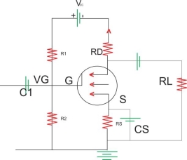
Figure 25: EMOSFET as an AMP
N-channel E-MOSFET Ampɤ
- It can operate with positive gate and drain Vtg where as in p-channel with –ve gate and drain Vtg
- For amplification MOSFET should operate in saturation region where the drain current ID remains constant
- The threshold Vtg (VT) is the minimum gate Vtg (VGS) required to induce the channel between source to drain
- Fig shows single stage common source ampɤ using Vtg bias method
- Vin is A.c. Signal
- Resistors R1 ,R2 and R5 provides the proper and stabilized operating point
- C in i/p coupling capacitor where is coat is the o/p coupling capacitor which blocks the d.c signal
- Cs is the bypass capacitor so that signal available at source terminal. Never pass through Rs otherwise o/p Vtg reduces.
Key Takeaways
- MOSFET is another type of field effect transistor. The MOSFET has become one of the most important devices used in design and construction computers
- MOSFET [metal oxide semiconductor field effect transistor]
- Type of MOSFET are Depletion type MOSFET, Enhancement type MOSFET and Power MOSFET
- Enhancement type MOSFET: classified in to two type n. Channel or p. Channel E MOSFET
- The operation can be explained with two different operating; Operation with VGS = 0 and Operation when VGS is +ve
- Vtg gain is given by

- MOSFET can act as a switch jest like a transistor a typical switching.
References:
1. Integrated Devices & Circuits by Millman & Halkias, TMH Publications.
2. Electronics Devices and Circuit Theory by R. Boylestad & L. Nashelsky, Pearson Publication
3. Electronic Communication System by G. Kennedy, TMH Publications.
4. Basic Electronics by Sanjeev Kumar & Vandana Sachdeva, Paragaon International Publication