Unit - 1
Introduction to LTI elements
Electronic systems are built around analog and digital components. They comprise resistors, capacitors, diodes, inductor, operational amplifiers and transistors. These components are often called active and passive elements. Majority of the analog circuits consist passive and active ones that are responsible for power management.
What is an Active element?
Active components control the charge flow in electronic circuits. It is the core component to operate any device. The two parameters to consider for proper device operation are current and voltage. Hence the voltage and current in a circuit may be boosted or stepped down based on the flow of electrons injected by an active device. Components like Diodes, Transistors, voltage operated devices, Vacuum tubes, voltage and current sources comes under active elements. An active component without doubt, amplifies the power of a signal (voltage or current). Transistor is a good example that acts as an amplifier in radio and RF circuits.
In addition, active elements are categorised into two sections. They are voltage controlled and current controlled sources. Voltage controlled devices produce their output current depending upon the input voltage. BJT (Bipolar junction transistor) is a voltage controlled device which supplies static voltage as a control signal.
What is Passive element?
Passive elements are quite opposite to active ones. They don’t require any external voltage to perform their job. Examples: Resistor, Capacitor, Inductor etc.
But they are not capable to provide energy on their own. They require assistance from active devices. For example, a resistor is a versatile component used as pull up or pulls down resistor in most of the hardware design.
We can use the pull-up and pull-down as control signal from the microcontroller interrupt to turn and turn off external devices. Inductors and capacitors have the capability to store energy for longer time and discharge.
Resistor

V=IR
P=I2R

Behaviour of Resistance:
Ac circuit containing pure resistance (R)
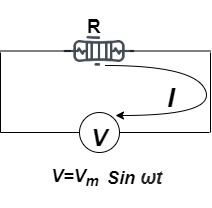
Fig: Circuit containing R
Consider Circuit Consisting pure resistance connected across ac voltage source
V = Vm Sin ωt ①
According to ohm’s law i =  =
= 
But Im = 
 ②
②
From ① and ② phase or represents RMD value.
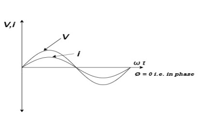
Fig: Waveform with element R
Power P = V. i
Equation P = Vm sin ω t Im sin ω t
P = Vm Im Sin2 ω t
P =  -
- 
Constant fluctuating power if we integrate it becomes zero

Average power
Pavg = 
Pavg = 
Pavg = Vrms Irms
Capacitors
Capacitor is a charge storing device (voltage)
Q ∝ V
Q = C V


AC circuit with a pure capacitance
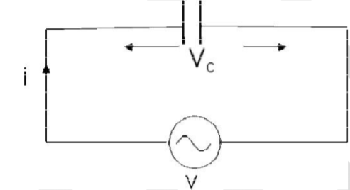
Fig: Circuit with pure Capacitance
Consider an AC circuit with a pure capacitance C as shown in the figure. The alternating voltage v is given by
V = Vm Sin ωt
 = Vm
= Vm  00
00
We can find the current through the capacitor as follows
q=CV
q= Cvm Sin ωt
 = ωCvm cos(ωt)
i= ωCvm cos(ωt)
i=im sin ( t+
t+ )
)
im= ωCvm
Xc = vm/im = 1/ωC
We observe that in a pure capacitive circuit, the current leads the voltage by 90⁰. Hence the voltage and current waveforms and phasors can be drawn as below.
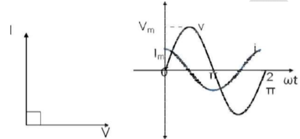
Fig: Phasor for C
Capacitive reactance
The capacitive reactance XC is given as
Xc= 1/2πfC
im = vm/Xc
Inductors
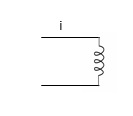
Based on electromagnetic induction
Faraday’s Law
Φ∝i
Φ = L.i


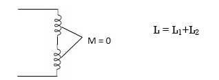

AC circuit with a pure inductance
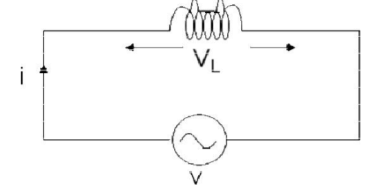
Fig: Circuit with pure inductance
Consider an AC circuit with a pure inductance L as shown in the figure. The alternating voltage v is given by
V = Vm Sin ωt
The current flowing in the circuit is i. The voltage across the inductor is given as VL which is the same as v. We can find the current through the inductor as follows
I=L 
Vm Sin ωt= L 
Di= Sin ωt
i = 

i =  sin (
sin ( t-
t- )
)
i= im sin ( t-
t- )
)
im = 
We observe that in a pure inductive circuit, the current lags behind the voltage by 90⁰. Hence the voltage and current waveforms and phasors can be drawn as below
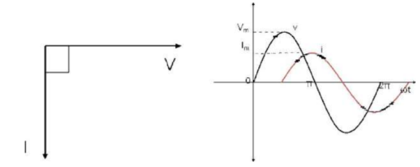
Fig: Phasor for Pure L
Inductive reactance
The inductive reactance XL is given as
XL = 2πfL
im = 
Key takeaway
Inductor do not respond any change as far as current is concerned.
Capacitor does not respond any change as far as voltage is concerned.
S.No. | Active Element | Passive Element |
1 | They require external power supply to operate | They do not require external power supply to operate |
2 | They have a function of gain | They do not have a function of gain |
3 | They produce energy in the form of voltage or current | They store energy in the form of voltage or current |
4 | Examples: Semiconductors, diodes and transistors | Examples: Resistor, capacitor and inductors |
Singularity functions are discontinuous functions or their derivatives are discontinuous. A singularity is a point at which a function does not possess a derivative. In other words, a singularity function is discontinuous at its singular points. Hence a function that is described by polynomial in t is thus a singularity function. The commonly used singularity functions are
Step Function,
Ramp Function, and
Impulse Function
The convolution theorem states that f1(t) and f2(t) are two time functions which are zero for t<0 and if Laplace transform are F1(s) and F2(s)then the transform of convolution of f1(t) and f2(t) is the product of individual transforms F1(s) and F2(s).
f(t) = f1(t)*f2(t) = 
= f2(t)*f1(t) = 
The convolution theorem of Laplace transform is
L[f1(t)*f2(t)] = L[f2(t)*f1(t)] = F1(s)F2(s)
The Laplace Transformation transforms convolution into multiplication.
The graphical presentation of the convolution integral helps in the understanding of every step in the convolution procedure. According to the definition integral, the convolution procedure involves the following steps:
1) Apply the convolution duration property to identify intervals in which the convolution is equal to zero.
2) Flip about the vertical axis one of the signals (the one that has a simpler form (shape) since the commutativity holds), that is, represent one of the signals in the time scale.
3) Vary the parameter from - to +
to + , that is, slide the flipped signal from the left to the right, look for the intervals where it overlaps with the other signal, and evaluate the integral of the product of two signals in the corresponding intervals.
1) Step Function:
U(t)=1 t≥0
=0 t<0
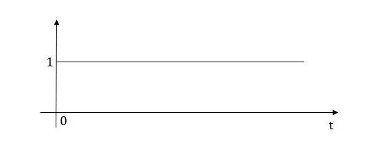
Fig: Step Signal
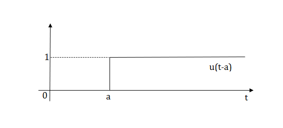
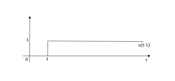
Fig: Shifted unit step signal
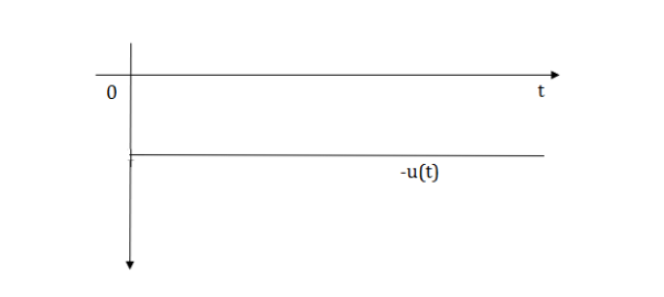
Fig: unit step signal -u(t)
2) Pulse Function:
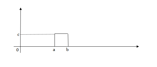
Fig: Pulse signal
L[u(t)]= =
=
f(t)<—>F(s)
f(t-a)= F(s)
F(s)
L[u(t-a)]=
Laplace transforms of pulse
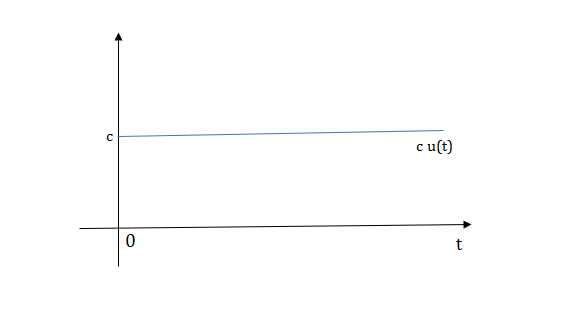
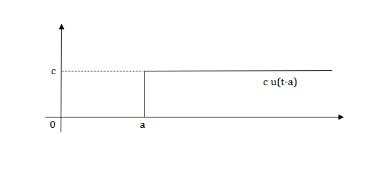
Fig: Shifted Pulse signal
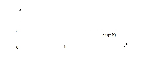
Fig: Shifted Pulse signal
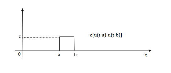
Fig: Final required Pulse signal
Q.1) Write equation for given waveform

Sol: 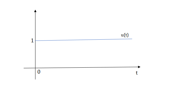
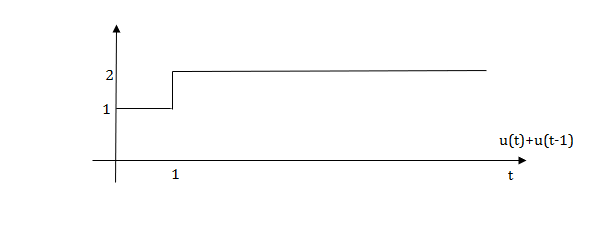
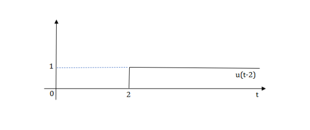
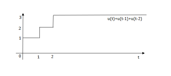
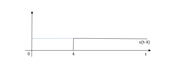
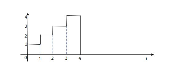
The final equation is=u(t)+u(t-1)+u(t-2)+u(t-3)-4u(t-4)
As the waveform is stopped at t=4 with amplitude 4,so we have to balance that using -4u(t-4).
Ramp function:
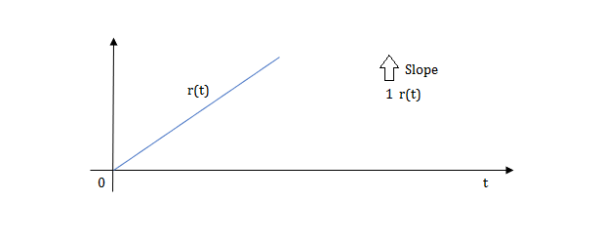
Fig: Ramp Function
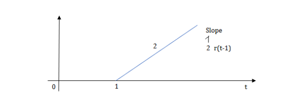
Fig: Shifted Ramp Function
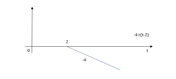
Fig: Shifted Ramp Function
L[r(t)] =
R(t)=tu(t)
R(t)=∫u(t)
Impulse Signal:
This signal has zero amplitude everywhere expect at the origin. Fig below shown the representation of Impulse signal.
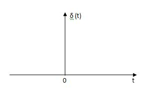
Fig: Impulse Function
The mathematical representations
A (t) = 0 for t ≠0
 dt = A e
Where A represent energy or area of the Laplace Transform of Impulse signal is
L [A (t) ]= A
The transfer function of a linear time invariant System is the Laplace transform of the impulse response of the system
Q) Write the equation for the given waveform?
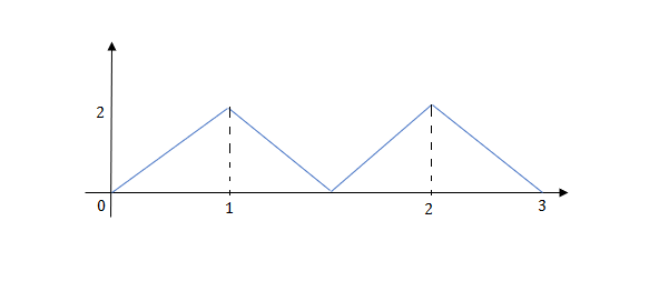
Sol: Calculating slope of above waveform
Slope for (0,0) and (1,2)
a1 slope= =2
=2
a2 slope= =-4
=-4
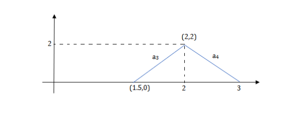
a3 slope =4 and a4= -2
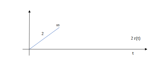
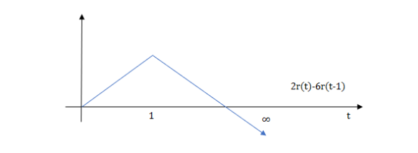
At t=1 slope changes from 2 to -4 so we need to add -6r(t-1) to 2r(t) to get the slope of -4.
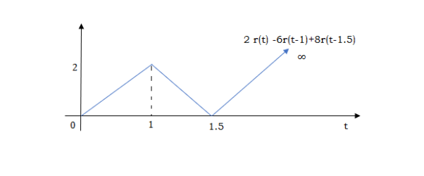
At t=1.5 slope changes from -4 to 4 so adding 8r(t-1.5) to get slope of 4
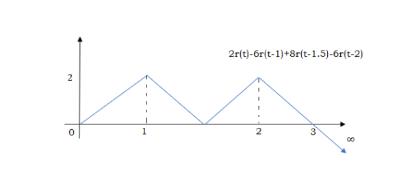
At t=2 slope changes from +4 to -2 so we add -6r(t-2). But we need to stop the waveform at t=3. Hence we have to make slope 0. Which can be done by adding +2r(t-3). Final equation is given as
2r(t)-6r(t-1.5)+8r(t-1.5)-6r(t-2)+2r(t-3)
Sinusoidal Waveform
Average Value:
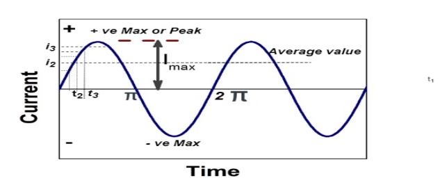
Fig: Sinusoidal waveform
The arithmetic mean of all the value over complete one cycle is called as average value

 =
= 
For the derivation we are considering only hall cycle.
Thus  varies from 0 to ᴫ
i = Im Sin


Solving
We get


Similarly, Vavg=
The average value of sinusoid ally varying alternating current is 0.636 times maximum value of alternating current.
RMS value: Root mean square value
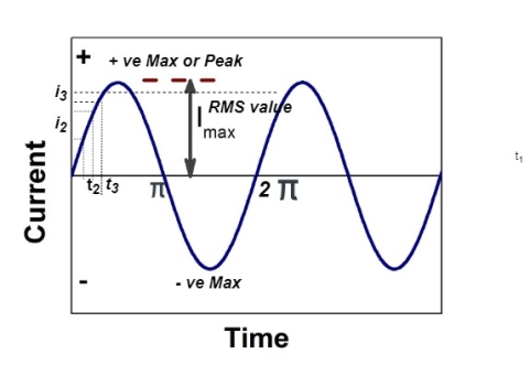
Fig: Sinusoidal waveform
The RMS value of AC current is equal to the steady state DC current that required to produce the same amount of heat produced by ac current provided that resistance and time for which these currents flows are identical.

I rms = 
Direction for RMS value:
Instantaneous current equation is given by
i = Im Sin 
But 
I rms = 
= 
=
=
Solving
=
=
Similar we can derive
V rms=  or 0.707 Vm
 the RMS value of sinusoidally alternating current is 0.707 times the maximum value of alternating current.
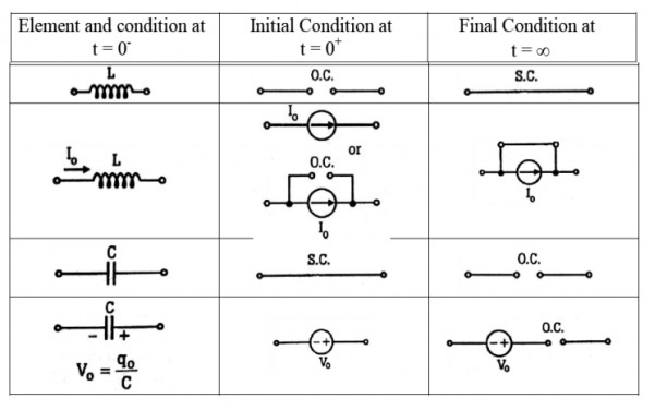
1.3 Behaviour of R, L and C at t=0+ and t=
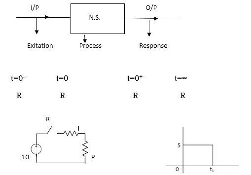
For R:
Time t=0- , time t=0-1 time t= infinity
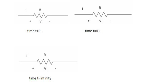
Fig: Behaviour of R for t=0-, t=0+ and t= infinity
# In the case of the capacitor:
At time t= 0-
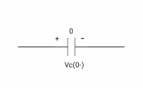
:. The capacitor is initially uncharged
Q (0-) =0
Q=cv
Q(0-) = cvc (0-)
Vc (0-) =0
At time t= 0+
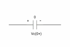
By low of conservation of charges
Q(0-) = Q(0+)
Cvc(0-) =cvc(0+)
Vc (0+) =0
Hence acts as

Fig: Capacitor when charged for t=infinity acts as SC
If the capacitor is initially uncharged at t= 0- then the voltage across the capacitor is zero at t=0+ capacitor will follow low of conservation of charges and Vc(0+) =0 it means at t=0+ capacitor behaves as a short circuit, in other words, the voltage across the capacitor cannot change instantaneously.
At time t= infinity,
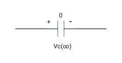

Fig: Capacitor fully charged behaves as OC
i = cdvc/dt constant and maximum
Hence, i= 0
At t= infinity, the capacitor will be fully charged or voltage across the capacitor is constant and current through the capacitor is zero so, the capacitor will behave as open –circuit
Say capacitor is initially charged
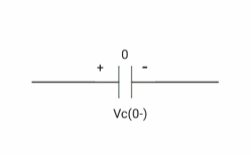
Q(0-) = Q(0+)
Cvc(0-) =cvc(0+)
V1 = Vc (0+)
At time t= 0-,

At time t= 0+,

At time t= 0+
It capacitor is initially charged at t= 0- as voltage across capacitor is V1 than at t=0+ inductor behaves as a voltage as a voltage source with value V1
At t=infinity

Fig: Capacitor fully charged behaves as OC
If the capacitor is initially charged and it is connected to any independent source for a long time than the current through the capacitor is zero and the capacitor will be fully charged and it behaves as OC.
For L
At t=0- the inductor is initially unenergized

Φ(0-) = 0
Φ = Li
Φ(0-) =L i(0-)
i(0-) = 0
At t=0+
By law of conservation of flux
Φ(0-) = Φ(0+)
L i(0-) = L i(0+)
i(0+) = 0
Hence acts as

If the inductor is initially unenergized or the initial flux is zero then the initial current through the inductor is also zero at t=0-. At t=0+ inductor will follow the law of conservation of flux and current through inductor at t=0+comes out to be zero which means that current through inductor changes instantaneously at t=0+ and it behaves as OC.
At time t = infinity
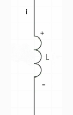
VL= Ldi/dt
VL= 0

At t= inductor will be fully charged or current through the inductor is maximum and constant and the voltage across the inductor is zero or inductor behaves as S.C.
If initially energized or has some flux or some initial current
At time t= 0-

At t=0+
By law of conservation of flux
Ø= Li =0
Ø(0)= Li(0-)
i(0-)= i(0+)
i(0+) = i1
Hence acts as
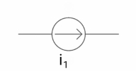
Fig: Behavior of inductor for t= 
If the inductor is initially energized at t=0- then at t=0+ it behaves as a current source because the current through the inductor cannot change instantaneously.
At t=  inductor will be fully energized the current through it will be maximum and constant and the voltage across the inductor is zero and behaves as SC
Key takeaway
The zero-input solution characterizes the natural response of the circuit. In other words, the zero-input solution is the solution when the circuit is energized at t = 0− and then left on this own (no external forcing). The question is to find the variation of the circuit variables or the evolution of the circuit variables under the KVL and KCL constraints, given the initial conditions. Stated differently the question is what is happening in the circuit due to the initial conditions in the absence of external input.
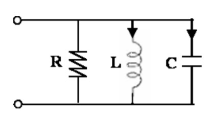
Fig: Zero-Input Parallel RLC Circuit
In resistive LTI circuits, the equation defining the solution of the circuit is a linear equation system. As we have noted before, the number of unknowns for such a description can be the number of nodes or the number of meshes. For resistive circuits with non-linear elements, the defining equation system is a non-linear equation. The non-linear relation is a quadratic equation if we have component with the relation V = i 2R.
The integral equations have certain advantages in terms of computation and there is a strong mathematical theory for the integral equations. In this course we prefer the differential equations descriptions for which there is an equally strong theory. (The differential equations can be more fundamental in equation writing since they describe the behaviour of the system via local differences.) The differential equation describing the circuit given in Figure is given as
(D2+ )VC(t) =
  D{is(t)}
When the input is(t) = 0 (zero-input), the equation characterizing the zero-input
(D2+ )VC(t) = 0
With VC(0+) = V0 and VC(0+) = -( )
)
The general solution for the following differential equation
(D2+2αD+ω02) VC(t)= 0
VC(t)= c
If this function is indeed the solution, then the differential equation should be satisfied for all t > 0. To check the guess, we insert the function into the differential equation and get the following equation
c (λ2 + 2αλ + ω02) = 0
The last equation shows that the guess is correct if c = 0 or λ2 + 2αλ + ω2o = 0. The solution c = 0 becomes VC(t) = 0 which cannot be the right solution the unless all initial conditions are zero. Thus, the non-trivial solutions should have λ which satisfies
(λ2 + 2αλ + ω02) = 0
This equation is called the characteristic equation of the system. The roots of the characteristic equation are called the natural frequencies. The roots can be written as follow
Natural Frequencies: λ1,2 = −α ±
The solution for the zero-input can then be written as follows
VC(t)= c1 +c2
+c2
Where λ1 and λ2 are the natural frequencies and c1 and c2 are the arbitrary constants.
Types of Zero-Input Responses:
The zero-input responses are categorized by the natural frequencies, that is the roots of the characteristic equation given above equation determine the type of response. The possibilities for the roots are
i. Distinct real roots (∆ > 0, i.e α > ωo)
Ii. Repeated real roots (∆ = 0, i.e. α = ωo)
Iii. Complex conjugate roots (∆ < 0, i.e. α < ωo)
The parameter α, which is 1/(RC) for the parallel RLC circuit, is called the damping factor. The parameter ωo, which is 1/ √ LC for the parallel RLC, is called the resonance frequency
α = 1/2RC
ωo = 1/ √ LC
Characteristic Equation: λ2 + 2αλ + ω2o = 0
α: Damping factor (1/sec, Hz.)
ωo: Natural frequency (1/sec, Hz.)
i. Overdamped Circuits (α > ωo):
The natural frequencies for the overdamped circuits are real valued and distinct. For the parallel RLC circuit with R = 1/5 Ω, L = 1/8 H and C = 1/2 F, we have α = 5 and ωo = 4. Since α > ωo, the response is overdamped, i.e. damping is greater than than ωo. The characteristic equation for this circuit is λ2+10λ+16 = 0 and the natural frequencies are λ = {−8, −2}.
The zero-input solution is then VziC(t) = c1e −2t + c2e −8t, t ≥ 0.
The constants c1 and c2 are to be determined according to the initial conditions at t = 0+.
Ii. Critically Damped Circuits (α = ωo): The natural frequencies for critically damped circuits are real valued and repeated. Let’s take R = 1/4 Ω, L = 1/8 H and C = 1/2 F, then α = ωo = 4 and the characteristic equation is λ2 + 8λ + 16 = 0. The natural frequencies are λ = −4.
The zero-input solution is then V ziC (t) = c1e −4t + c2te−4t, t ≥ 0.
Iii. Underdamped Circuits (α < ωo): The natural frequencies for critically damped circuits are complex valued and two natural frequencies are the complex conjugates of each other. Let’s take R = 1/3 Ω, L = 1/8 H and C = 1/2 F in the parallel RLC circuit, then α = 3 and ωo = 4. It is clear that the damping coefficient smaller than the natural frequency, hence the name underdamped. The characteristic equation for this system is λ2 + 6λ + 16 = 0. The natural frequencies are λ = −3 + j √ 7, −3 − j √ 7.
The zero-input solution is then: VziC(t) = c1e (−3−j √ 7)t + c2te(−3+j √ 7)t
Zero-State Response
The zero-state solution assumes the circuit is not energized initially, that is the initial voltage of all capacitors and the initial current of all inductors are zero. The zero-stage solution is the response due to the applied input in the absence of any initial conditions, that is when the system is at rest initially. The general approach is as follows:
i. Find the initial conditions at t = 0+ by inspecting the t = 0+ circuit.
Ii. Solve the differential equation for t > 0 with the t = 0+ initial conditions.
For the zero-state solution, the circuit is initially at rest; therefore t = 0− values for the capacitor voltages and inductor currents are zero. From our earlier discussions, we know that the capacitor voltages and inductor currents is a continuous function of time if the input is bounded. As discussed before, this is a consequence of the terminal equations for the capacitor (VC(t) = VC(0)+1/C ∫ IC(t ′ )dt′ ) and the inductor (IL(t) = IL(0)+1/L ∫VL(t ′ )dt′ ). Therefore, if there is no impulsive source in the circuit, VC(0+) = VC(0−) and IL(0+) = IL(0−) is granted. The continuity of the VC(t) and IL(t) is the golden rule that should always be remembered.
Below we find the zero-state response to ramp, unit step and impulse input. The method shown below can also be used to directly write the complete solution, i.e. solving a circuit without zero-input and zero-state decomposition. As we have discussed before, this decomposition enables us to apply the superposition for the zero-stage responses. Therefore, it is very useful if we have a superposition of elementary functions at the input. In this case, the zero-state response to the superposed input is the superposition of zero-state responses to each input. This is the reason (the possibility of superposition) that makes the zero-state responses important to us.
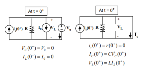
Fig: At t=0+ circuit for ramp input
i. Ramp Response:
Figure above shows the circuit at t = 0+ when the input is the ramp function. An inspection of this circuit, reveals that all circuit variables in this current has the value of zero t = 0+, that is IC(0+) = 0 and therefore VC(0+) = 0. Hence the t = 0+ initial conditions for the ramp input is VC(0+) = V˙C(0+) = 0 and the first step of the procedure given above is completed. The differential equation for the ramp input, i.e. is(t) = r(t) is as follows
(D2+ )VC(t) =
  D{is(t)} =
  u(t)
u(t)
For t > 0, the differential equation is
(D2+ )VC(t) =
The zero-state solution is then
VzsC(t) = L + c1e λ1t + c2e λ2t, t > 0
Here λ1, λ2 are the natural frequencies and the constants c1, c2 should be selected the meet the initial conditions at t = 0+.
Ii. Step Response: Figure shows the circuit at t = 0+ when the input is the step function.
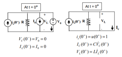
Fig: At t = 0+ circuit for the unit step input
A simple analysis of the t = 0+ which does not contain any dynamic elements, but only sources and resistors reveals that VC(0+) = 0 and VC(0+) = 1/C. It should be noted that VC(0+) is due to the continuity of the capacitor voltage for the bounded inputs (the golden rule!) and does not follow from any analysis. Then the differential equation for the unit step input, i.e. is(t) = u(t) is as follows
(D2+ )VC(t) =
  D{is(t)} =
 (t)
(t)
On the right hand side of the differential equation we have a δ(t) function which is quite a problem if we were presented with such a differential equation at a differential equations course; but note that for t > 0, the differential equation is
(D2+ )VC(t) =0 [for t>0]
The zero-state solution for t > 0, is then
VzsC(t) = c1e λ1t + c2eλ2t, t > 0
Here λ1, λ2 are the natural frequencies and the constants c1, c2 should be selected the meet the initial conditions at t = 0+.
Iii. Impulse Response: Figure shows the circuit that is be analysed for VC(0+) and VC(0+) values.
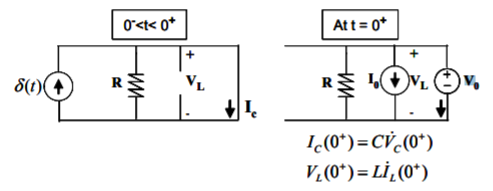
Fig: At t = 0+ circuit for the impulse input
The input is not a bounded one, therefore we cannot apply the rule stating that the capacitor voltage and inductor current is continuous. The circuit on the left side of Figure shows that IC(t) = δ(t) “during the application of the impulse”. Hence VC(0+) = VC(0−) + 1/C  = 1/C. To find IL(0+), we need to find VL(t) during the application of the impulse. It can be noted from Figure that VL(t) = 0 in between 0− and 0+ and hence IL(0+) = 0.
To solve the differential equation written for VC(t), we need the initial conditions for VC at t = 0+. To find VC(0+), we examine t = 0+ circuit, which is the circuit just after the application of the impulse. This circuit is given on the right side of Figure. In this circuit V0 = 1/C and I0 = 0. Then a resistive circuit analysis reveals that IC(0+) = −VC(0+)/R = −1/(RC), then V˙C(0+) = −1/(RC2 ). We are done with the finding of the initial conditions.
The differential equation for the unit impulse input, i.e. is(t) = δ(t) is as follows
(D2+ )VC(t) =
  D{is(t)} =
 (t)
(t)
The differential equation reduces to
(D2+ )VC(t) =0
The zero-state solution for t > 0, is then
VzsC(t) = c1e λ1t + c2e λ2t, t > 0
Here λ1, λ2 are the natural frequencies as before and the constants c1, c2 should be selected the meet the initial conditions at t = 0+
Complete response of transient behaviour of RL, RC and RLC circuits using integrodifferential equation
A linear differential equation which describes any circuit has two parts in its solution, one is complimentary function and other is particular solution. The complimentary solution gives the transient response and the particular solution deals with steady state response. The complete or total response of network is the sum of the transient response and steady state response which is represented by general solution of differential equation.
First order homogenous differential equation.


Integrating both sides
y(t)=k
First order non homogenous differential equation


Integrating above equation we get
y(t) =∫ Q
=∫ Q 
y(t)= ∫ Q
∫ Q 
The first term of above solution is known as particular Integral and second is known as complementary function.
FOR RL Circuit
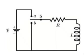
Fig: Series RL circuit
After switch is closed applying KVL
 =0
=0
This is first order homogeneous differential equation so
 dt
dt
Integrating both sides
Ln i=  t+K
t+K
Taking antilog of both sides
i=k
At t=0
i(0)= =I0
=I0
 =ke0
=ke0
The particular solution is given as
i=  for t≥0
= for t<0
FOR RC Circuit
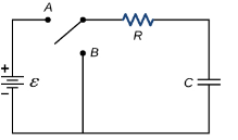
Fig: Series RC circuit
 =V
=V
For t>0 applying KVL
Ri(t)+ +V=0
+V=0

Hence general solution of above equation is calculated same as for RL circuit
i=k
i(0)=- 
Hence, particular solution for network is given as
i=-  for t for t≥0
= for t<0
Time constant for RL circuit
From above section for RL circuit at t≥0
i= 
i=I0
I0= 

Time taken for current to drop from unity to zero is called as time constant T.

 sec
sec
FOR RC Circuit
It can be calculated in the same manner as for series RL circuit
The time constant is given as 
T=RC
The network equations can be written for knowing the current or voltage of any branch or element in the given circuit. The equations can be voltage equations or current equation for the circuit given.
The voltage equations are written as
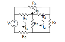
Fig: Circuit for loop analysis
For Loop 1 with il

For Loop 2 with i2

For Loop 3 with i3

The current equations are written as
For these we assume every node as a voltage point and write the current equation for every element. For current source, current entering is negative.
Examples
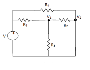
Fig: Circuit for Node analysis
For node V1

For node V2

For V

Example: Using nodal analysis find voltage across 5resistor.
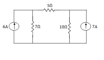
Solution:
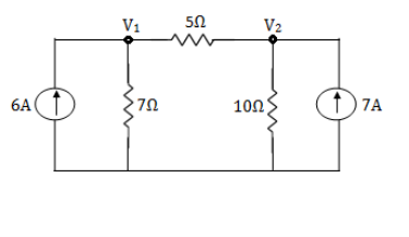
For V1


 1
1
For V2


 2
2
Solving 1 and 2:


For 5 voltage = 
= -50.9 + 57.27
= 6.37V
Que Write the loop equations for the given circuit below?
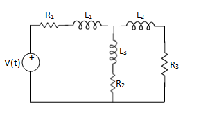
Solution:
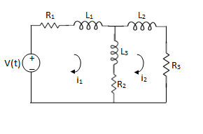
For loop 1

For loop 2

Q) Use mesh equations to find iA for the circuit given below?
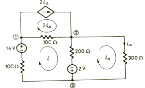
Sol: For loop with current I the equations will be
100i+100(i-2iA)+200(i-iA)-2-14=0
400i-400 iA=16……….(1)
Equation for loop with current iA
2+200(iA-i)+300 iA = 0
-200i+500 iA= -2………(2)
Solving above equations we get
i=60mA
iA = 20mA
Q) Write the integro-differential equation for the loop currents shown below.
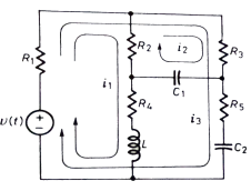
Sol: Equation for loop 1 with current i1
v(t)=(R1+R2+R4)i1 +L -R2 i2+ R5i3
Equation for loop 2 with current i2
-R2i1+(R2+R3) i2 + +R3i3 = 0
Equation for loop 3 with current i3
V(t) = R1i3+R3i3+(R1+R3+R5) i3+
Q) For the given network write the integro differential equation?
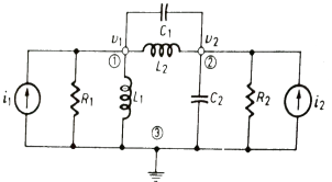
Sol: Let V1 and V2 be the node voltages.
Equation for node v1 will be
 +
+ +
+ +C1
+C1 = i1
= i1
 + C2
+ C2 + C1
+ C1 +
+ = i2
= i2
Q) In network below switch is moved from 1 to 2 at t=0 a steady state is achieved already. Fond capacitor voltage Vc(t) and current i(t) through 200Ω?
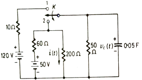
Fig: Circuit Diagram
Sol: The Voltage across capacitor is given by
Vc(t)= K1+K2 
The steady state is reached when t= the above equation becomes
Vc( )= Lt t-->
 K = K1
At t=0
Vc(0)= K1+K2
K2= Vc(0)- Vc( )
)
The final response for the circuit is given as
Vc(t)= Vc( )-[Vc(
 )-Vc(
)-Vc( )]
)]
When switch is at position 1
Vc(0)=  x 50 = 100V
So, voltage of capacitor at t=0 and t=0+ will remain same.
TO find Req we replace voltage source by short circuit
Req = 60||200||50 = 24 Ω
The time constant will be T = ReqC = 24x0.05 = 1.2sec
Switch at position 2
The steady state voltage across capacitor is given by
 =
=  +
+ 
Vc( ) = 20V
The complete response will be
Vc(t)= Vc( )-[Vc(
 )-Vc(
)-Vc( )]
)]
Vc(t)= 20 –[20-100]
Vc(t)= 20+ 80 
The value of current at switch position 1
I= 50/(200+60) = 0.192A
When switch is at 2
i(0+) = 100/200= 0.5A
i( ) = Vc(
 ) /200 = 0.1A
The complete response of current is
i(t)= i( )-[i(
)-[i( )-i(
)-i( )]
)]
i(t)= 0.1-[0.1-0.5]
i(t)=0.1+0.4
Ques Find the value of V0(t) for circuit below?
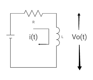
Sol:
Time constant, c= L/Req = L/R
V( ) = 0
) = 0
V(0) = VR
i( ) = VR/R
i(0) =0
By KVL,
VR=i(t) R + L di/dt(t)
On solving
V0(t)= VR e-tR/L
Ques Find iL(t) for the circuit below. For t>0?
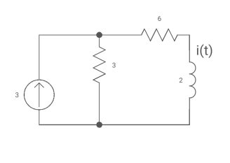
Sol: The circuit for Req will be
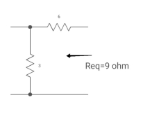
Fig: Circuit for Req
Req = 6+3
= 9ohm
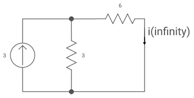
Fig: Circuit when inductor acts as short circuit
T= L/Req = 2/9 sec
i(0) =0
i( ) = 3*3/6+3 = 1A
i(t) = 1 [1-e4.5t]
Ques Capacitor is initially uncharged find Vc (t); t >0
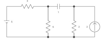
Fig: Circuit Diagram
Sol:
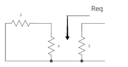
Fig: Circuit for Req
Req = (3116)+2
=2+2 = 4ohm
T= C Req= 2 sec
Clearly Vc(0) =0
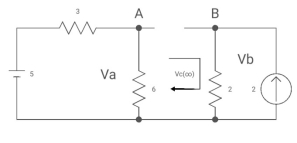
Fig: Circuit when capacitor acts as open circuit
By voltage divides, VA = 5*6/3+B = 30 v/9
Clearly by ohms low
VB = 2*2 = 4v
Apply KVL, VA-Vc-VB =0
Vc( ) = 30/9 – 4 = -2/3 V
Vc (t) = -2/3 [1- e0.25t]
CURVE:
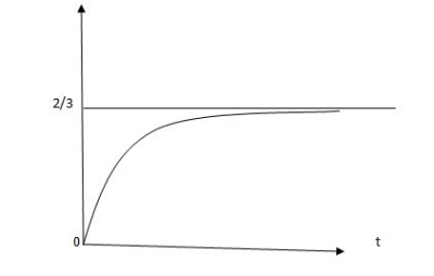
Vc(t) =2/3 [1-e-0.5t]
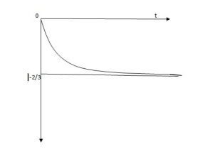
Fig: Response for above circuit
Vc(t) = -2/3 [1-e-0.5t]
Ques Find i(t) for the given circuit below?
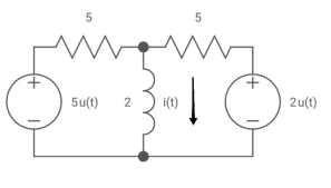
Sol: We know i(t) = i ( ) +[i(0)- i(
 )] e-t/T
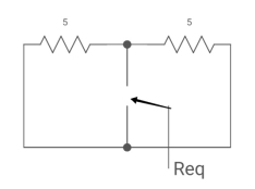
Fig: Circuit for Req
Req = 5*5/5+5 = 5/2 ohm
T=L/Req = 4/5 sec
Also
i(0) =0
i( ) = u(t) +2/5 u(t)
i(t) = 1.4 [1-e-5/4t)]u(t)
Ques: If switch ‘s’ closed for long time before opening at t=0-. Find Vx (0+)?
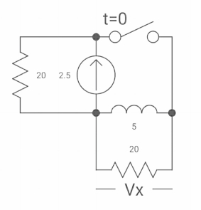
Fig: Circuit diagram
Sol: At t= 0- switch was closed,
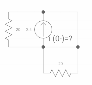
Fig: Switch is open
iL(0-) = 2.5A
At t= 0+
Inductor is initially charged so iL(0-) = iL(0+)
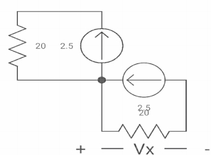
Fig: when switch is closed for long
-Vx = 20x2.5
Vx = -50A
Ques: Find VR(0+) and dil/dt(t) = 0+ If switch is opened at t= 0?
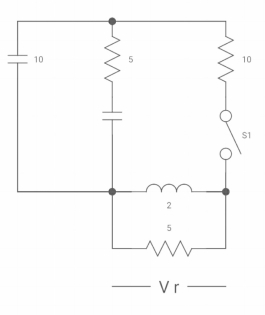
Sol: At time t=0-
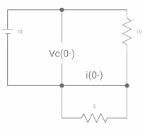
Fig: Capacitor SC switch closed for long
At t=0-
Vc(0-) = 10V
IL(0-) = 10/10 = 1 A
Also, iL(0-) = iL(0+) = 1A
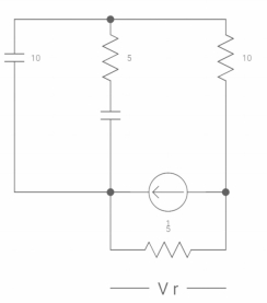
VR(0+) = 5V
Ldi(t)/dt = VL (t)
DiL(t)/dt = VL(t)/L
At t= 0+
d iL (0+) /dt = VL(0+)/L
-VL (0+)-VR =0
VL (0+) = -5V
DiL(t)/dt at t=0+
VL(0+)/L =-5/2
Dil/dt(o+) = 2.5 A/s
Ques: Find Vc(o+) and iR (o+) it switch‘s’ is closed at t=0?

Sol: At t=0-
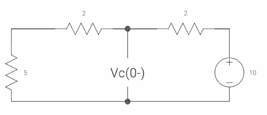
Fig: When switch opened at t=0
As capacitor is fully charged so acts as open circuit
Vc (0-) = 7*10/7+2 = 70/9v
At t=0+
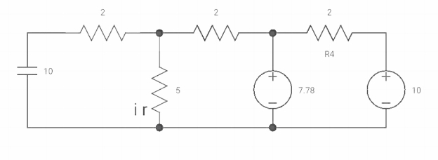
Fig: At t=0+ circuit
Vc(0+) = Vc (0) = 40/9v
By applying kcl at A,
VA-10/2+ VA/5+VA-7019/2 =0
VA [1/5+1/2+1/2] = 5+35/9
Va [6/5] = 80/9
Va= 400/54v
IR (0+) = Va/5 = 400/54*5 = 80/54 A
Q) Find diL(t)/dt and dVc(t)/dt at t=0+. If switch is opened at t=0?
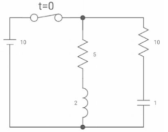
Sol: At t=0-
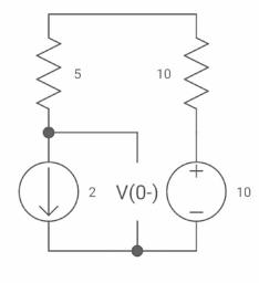
Fig: Switch closed for long
Vc(0-) =10V = Vc(0+)
iL(0-) = 2A
DiL(t)/dt = VL(t)/L
At t=0+
DiL(0+)/dt = VL(0+)/L
Similarly, C = ic(t)
 = ic(t)/C
At t=0+
 = ic(0+)/C
ic(0+) = -2A
Complete response of transient behaviour of RL, RC and RLC circuits using Laplace Transform
Analysis of electrical circuits using Laplace Transform for standard inputs
LAPALACE TRANSFORM:
If LT[f(t)]= F(s)
Where F(s)= dt
dt
f(t) F(s)
F(s)

 sF(s)-f(0-)
 f(t)
f(t) S2F(s)-sf(0-)-f’(0-)
Now, we find Laplace for 
 =
= +
+
Now if f(t)=ic(t) [current through capacitor]
 =
= +
+
 =
= +
+
=[q(0)-q( )]+
)]+
=[q(0)-0]+
Multiplying both sides by 1/C
 =
= +
+
Vc(t)= +
+
Vc(t)=Vc(0)+
By Laplace Transform
Vc(s)= +
+
Vc(s)= +
+
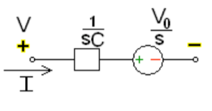
Fig: Laplace transformed circuit for C
Now by source conversion
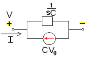
Fig: Source transformed circuit for C
 =
= +
+
Now if f(t)=VL(t) [voltage across inductor]
 =
= +
+
 =
= +
+
= -
- ]+
]+
= -0]+
-0]+
Multiplying both sides by 1/L

 =
= +
+
iL(t)=iL(0)+
By Laplace Transform
IL(s)= +
+
IL(s)= +
+
NOTE: Voltage------->Series circuit
Current------->Parallel circuit
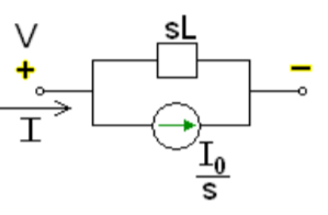
Fig: Laplace transformed circuit for L
By source transformation
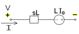
Fig: Source transformed circuit for L
Current through capacitor
iC(t)=
IC(s)=C[sVc(s)-Vc(0)]
Vc(s)= +
+
Voltage about inductor,
VL(t)=
VL(s)=L[sIL(s)-iL(0)]
IL(s)= +
+
Examples
Que For given RL circuit find the differential equation for current i?

Fig: Series RL circuit
After switch is closed applying KVL
 =0
=0
This is first order homogeneous differential equation so
 dt
dt
Integrating both sides
Ln i=  t+K
t+K
Taking antilog of both sides
i=k
At t=0
i(0)= =I0
=I0
 =ke0
=ke0
The particular solution is given as
i=  for t≥0
= for t<0
Ques: Find IL(0) for the given circuit below
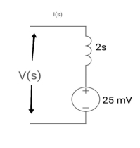
Sol: From above circuit
L = 2H
LiL (0) = 25 mv
IL (0) = 12.5 m A
Que: Find value across capacitor?
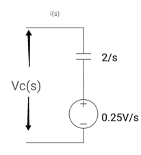
Sol: From above circuit we can write
1/cs = 2/s
C=1/2f
Vc (0)/s = 0.25v/s
Vc(0)= .25v
Ques: Find voltage across capacitor?
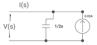
Sol: 1/cs = 1/2S
C=2F
CVc (0) = 0.02
Vc(0)= 0.01V
Que:
(a) switch is at before moving to position = at t= 0, at t= 0+, i1(t) is
(a) –V/2R (b) –V/R (c) – V/4R

Sol:
I1(t) L.T I1(s)
I2(t) L.T I2(s)
Then express in form
[ I1(s)/I2(s)] [::] = [:]
Drawing the ckl at t = 0-

:. The capacitor is connected for long
Vc1(0-)= V
iL(0-) =0
Vc2(0-)=0
At t= 0+


i1 (0+) = -V/2R
For t>0 the circuit is
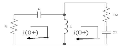
Apply KVL
-R i1(t) -1/c  dt -L
dt -L =0
=0
Also, we can deduce i1(t)- i2 (t) = iL(t)
-Ri1(t) -1/c  - L
- L = 0
= 0
-RI1(s)-[ -
- ]-L[sI1(s)-iL(0-)]=0
- RI1(s)- -
-  -s L I2(s)=0
 - s L I2(s)= -
  (1)
(1)
Again
-Ri2(t) ) -1/c  dt -L
dt -L =0
=0
-Ri1(t) -1/c  - L
- L = 0
= 0
Taking Laplace Transform
-RI2(s)- [ -
- ]- L[s IL(s)- iL(0-)]=0
-RI2(s)-  -
- Ls[ I1(s)- I2(s)]=0
 - s L I1(s)=0 (2)
Hence in matrix representation

 =
= 
Ques: All initial conditions are zero i(t) L.T, I(s), then find I(s)?
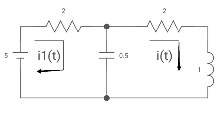
Sol: Drawing Laplace circuit
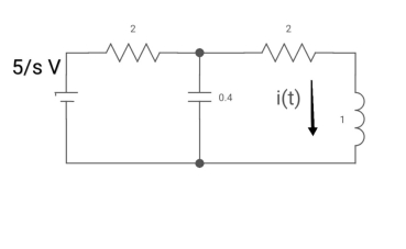
(2+S) 11 2/S
Zeq = [(2+S)2/S]/[2+S+2/S]=[2(S+2)]/[S2+2s+2]

V1(s) = [5/S{2(S+2)/S2+2S+2}]/[2+{2(S+2)/ S2+2S+2}]
V1(s) = [5(S+2)/S]/[S2+ 3S +4]
I(s) = V1(s)/(S+2) = (5/S)/(S2+35+4)
Initial and Final Value Theorem
The initial value theorem

This theorem is valid if and only if f(t) has no impulse functions.
The final value theorem

This theorem is valid if and only if all but one of the poles of F(s) are in the left-half of the complex plane, and the one that is not can only be at the origin.
Steps for Laplace transform circuit analysis:
1. Redraw the circuit (nothing about the Laplace transform changes the types of elements or their interconnections).
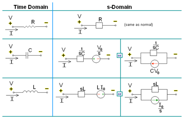
2. Any voltages or currents with values given are Laplace transformed using the functional and operational tables.
3. Any voltages or currents represented symbolically, using i(t) and v(t), are replaced with the symbols I(s) and V(s).
4. All component values are replaced with the corresponding complex impedance, Z(s).
5. Use DC circuit analysis techniques to write the s-domain equations and solve them. Check your solutions with IVT and FVT.
6. Inverse-Laplace transform s-domain solutions to get time domain solutions. Check your solutions at t = 0 and t = .
Transformed network with initial conditions
Que: The switch is at before moving to position = at t= 0, at t= 0+, i1(t) is
(b) –V/2R (b) –V/R (c) – V/4R (d) 0
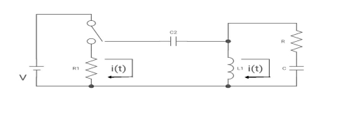
Sol:
I1(t) L.T I1(s)
I2(t) L.T I2(s)
Then express in form
[ I1(s)/I2(s)] [::] .[:]
Drawing the ckl at t = 0-
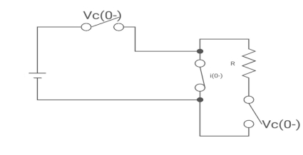
Fig: circuit at t=0-
:. The capacitor is connected for long
Vc1(0-)= V
iL(0-) =0
Vc2(0-)=0
At t= 0+
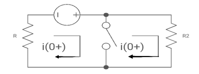
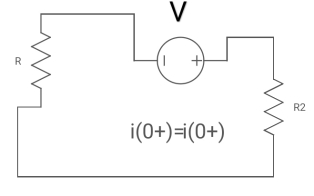
Fig: Circuit at t=0+
i1 (0+) = -V/2R
For t>0 the circuit is

Fig: KVL in Circuit
Apply KVL
-R i1(t) -1/c  dt -L
dt -L =0
=0
Also, we can deduce i1(t)- i2 (t) = iL(t)
-Ri1(t) -1/c  - L
- L = 0
= 0
-RI1(s)-[ -
- ]-L[sI1(s)-iL(0-)]=0
- RI1(s)- -
-  -s L I2(s)=0
 - s L I2(s)= -
  (1)
(1)
Again
-Ri2(t) ) -1/c  dt -L
dt -L =0
=0
-Ri1(t) -1/c  - L
- L = 0
= 0
Taking Laplace Transform
-RI2(s)- [ -
- ]- L[s IL(s)- iL(0-)]=0
-RI2(s)-  -
- Ls[ I1(s)- I2(s)]=0
 - s L I1(s)=0 (2)
Hence in the matrix representation

 =
= 
Ques: All initial conditions are zero i(t) I(s), then find I(s)?

Sol: Drawing Laplace circuit

(2+S) 11 2/S
Zeq = [(2+S)2/S]/[2+S+2/S]=[2(S+2)]/[S2+2s+2]
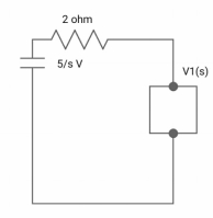
V1(s) = [5/S{2(S+2)/S2+2S+2}]/[2+{2(S+2)/ S2+2S+2}]
V1(s) = [5(S+2)/S]/[S2+ 3S +4]
I(s) = V1(s)/(S+2) = (5/S)/(S2+35+4)
Que) There is no initial energy stored in this circuit. Find i1(t) and i2(t) for t>0?
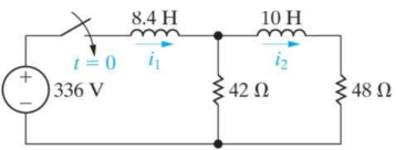
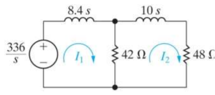
Sol:

When circuit is closed the network is shown


Que) Find v0 (t) for t > 0.
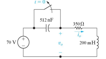
Sol: Taking Laplace transform of above circuit we have,
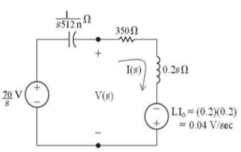
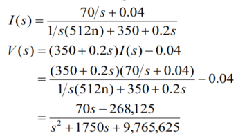
Que) There is no initial energy stored in this circuit. Find vo if ig = 5u(t) mA.
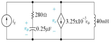
Sol: Laplace Transform of above circuit we get
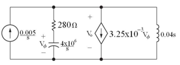

By voltage division we get


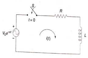
Que) Find value of current i(t) for the given circuit?
Sol:
Applying KVL we get

Taking Laplace transform of above equation we get

There is no initial current in inductor before closing the switch so i(0+)=0.


Taking ILT we get

Que) For the circuit shown below find the value of i1(t) and i2(t) and output voltage across 5 Ohm resistor when the switch is closed also find initial and final values of current?
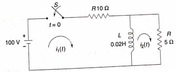
Sol: By KVL we have

Taking LT of above equations, we get

Solving above equation we get


By inverse Laplace transform we get
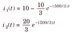
The voltage across 5 Ohm resistor is

The initial value of i1(t) is

The final value of i2(t) is

The initial value of i2(t) is

The Final value of i2(t) is

References:
- M. E. Van Valkenburg, “Network Analysis”, Prentice Hall, 2006.
- D. RoyChoudhury, “Networks and Systems”, New Age International Publications, 1998.
- W. H. Hayt and J. E. Kemmerly, “Engineering Circuit Analysis”, McGraw Hill Education, 2013.
- C. K. Alexander and M. N. O. Sadiku, “Electric Circuits”, McGraw Hill Education, 2004.
- K. V. V. Murthy and M. S. Kamath, “Basic Circuit Analysis”, Jaico Publishers, 1999.