Unit - 3
MOSFET circuits
A MOSFET is the common transistor used in digital circuits. It can be made with either p-type or n-type semiconductors, complementary pairs of MOS transistors can be used to make switching circuits with very low power consumption, in the form of CMOS logic.
MOSFETs are particularly useful in amplifiers due to their input impedance being nearly infinite which allows the amplifier to capture almost all the incoming signal.
MOSFETs are available in two basic forms:
- Depletion Type: The transistor requires the Gate-Source voltage (VGS) to switch the device “OFF”. The depletion-mode MOSFET is equivalent to a “Normally Closed” switch.
- Enhancement Type: The transistor requires a Gate-Source voltage(VGS) to switch the device “ON”. The enhancement-mode MOSFET is equivalent to a “Normally Open” switch.
Structure:
It is a four-terminal device with source(S), gate (G), drain (D) and body (B) terminals. The body is frequently connected to the source terminal, reducing the terminals to three. It works by varying the width of a channel along which charge carriers flow (electrons or holes).

Figure 1. MOSFET has a vertically oriented four-layer structure.
- The p-type middle layer term as the body.
- The n– layer is the drift layer.
- This layer is lightly doped as compared to the drain and source layer.
- The breakdown voltage of power MOSFET determines from the width of the drift layer.
- First and last both layers are an n+ layer. First layer is the source layer and the last layer is the drain layer.
The charge carriers enter the channel at source and exit via the drain. The width of the channel is controlled by the voltage on an electrode is called gate which is located between source and drain.
A p-channel MOSFET structure has exactly opposite doping profile.
- The GATE terminal is not directly connected with p-type, there is an oxide layer between the metal and semiconductor.
- This oxide layer act as a dielectric layer between the metal and the semiconductor. It forms a MOS (metal oxide semiconductor) capacitance at the input of the MOSFET.
- This capacitance is large (>1000 pF). The oxide layer gives good insulating property by providing the SiO2 layer that isolates the gate terminal from the body layer.
V-I characteristics
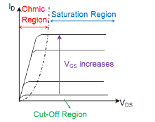
Figure 2. V-I characteristics of MOSFET
It has three regions: saturation, cut-off, and ohmic region.
- When the gate-source voltage is less than the threshold voltage, the MOSFET is in the cut-off state. To avoid breakdown the drain to source breakdown voltage should be greater than the applied voltage. The avalanche breakdown takes place.
- When the gate-source voltage is greater than threshold the power MOSFET goes into the ohmic region and the drain to source voltage is small. In this region, the power dissipation is low.
- In the saturation region, the drain current is almost independent of the drain to source voltage. It is only dependent on the gate to source voltage. The gate voltage is greater than the threshold voltage. The drain current increase with the increase in the gate to source voltage.
The drain terminal (D) of the MOSFET is connected to the supply voltage VS via the drain resistor RD while its source terminal (S) is grounded. It has an input voltage Vi applied at its gate terminal (G) while the output Vo is drawn from its drain.
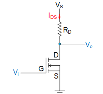
Figure 3. n-channel Enhancement MOSFET functioning as a switch
- When Vi = 0V, which means the gate terminal of the MOSFET is left unbiased. As a result, the MOSFET will be OFF and operates in its cut-off region wherein it offers a high impedance path to the flow of current which makes the IDS almost equivalent to zero.
- As a result, even the voltage drop across RD will become zero due to which the output voltage Vo will become almost equal to VS.
When Vi > VT under this condition, the MOSFET will start to conduct and if the VS provided is greater than the pinch-off voltage VP of the device then the MOSFET starts to operate in its saturation region. - The device will offer low resistance path for the flow of constant IDS, almost acting like a short circuit. As a result, the output voltage will be pulled towards low voltage level, which will be ideally zero.
Thus, the output voltage alters between VS and zero depending on whether the input provided is less than or greater than VT, respectively. Thus, it can be concluded that MOSFET can be made to function as electronic switches when made to operate between cut-off and saturation operating regions.

Figure 4. MOSFET as as Amplifier
This is a conceptual amplifier for two resons:
- The bias with VGs is impractical.
- In ICs large valued resistors take up too much physical space.
To operate as small -signal amplifier we bias MOSFET in saturation region. For analysis of DC operating point we set vgs =0 so that
ID = ½ Kn’ W/L (vgs -Vt) 2 --------------------(1)
From the circuit VDS = VDD – ID RD ------------------------------(2)
For operation in saturation region
VGD ≤ Vt ------ vgs – vds ≤ Vt
Or vds ≥ vgs – Vt --------------------------------------------------(3)
Where the total drain to source voltage is
Vds = Vds + vds
(bias) AC
With an AC signal applied at the gate
Vgs = VGS + vgs -------------------------------(4)
Substituting (4) in (1) we get
ID = ½ kn’ W/L (VGS + vgs – Vt) 2 = ½ kn’ W/L (VGS – Vt) + vgs ] 2 ----------(5)
= ½ kn’ W/L (VGS – Vt) 2 + 2/2 kn ‘ W/L (VGS – Vt) vgs + ½ kn’ W/L v 2 gs ---------(6)
The last term is non linear in vgs which is not desorable for linear amplifier. Hence for linear operation the last term should be small with respect to linear term and the second term is proportional to vgs.
Or vgs<< 2 (VGS – Vt) ------------------------------------------(7)
If this small signal condition (7) is satisfied then from (6) the total drain current is a approximately linear summation.
iD ͌ ID + i d --------------------------------------------------------------(8)
Where
Id = kn’ W/L (VGS – Vt) vgs ‘ ---------------------------------------(9)
From this expression (9) we see that AC drain current id is related to vgs by transistor transconductance gm.
Gm = id / vgs = kn’ W/L (VGS – Vt) [S]
Which is sometimes expressed in terms of overdrive voltage VoV = Vgs – Vt
Gm = kn’ W/L Vov [S]
In saturation mode the MOSFET acts as a voltage controlled device . The control voltage is vgs and output current is id which gives rise to small signal model π model.
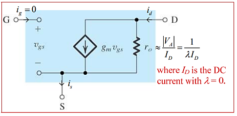
Figure 5. Small signal model of MOSFET
Ig=0 and vgs ≠ 0 the infinite input impedance
Ro models the finite output resistance .
We know that gm = k’n W/L (Vgs – Vt)
Hence it can be shown that
Gm = 2Id/ Vov = Id / (Vgs – Vt) /2
Biasing circuits
N-channel enhancement mode MOSFET circuit shows the source terminal at ground potential and is common to both the input and output sides of the circuit. *The coupling capacitor acts as an open circuit to d.c. But it allows the signal voltage to be coupled to the gate of the MOSFET
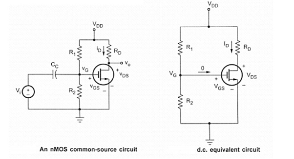
Figure 6. Biasing circuit
As Ig = 0 in VG is given as,
VG = VGS = (R2/R1+R2) VDD
Assume VG > VT , MOSFET is biased in the saturation region, the drain current is,
ID = K(VGS – VT) 2
Applying KVL to drain current we have
VDS = VDD – ID RD
If VDS > VDS (sat) = VGS – VT the the MOSFET is biased in the saturation region.
If VDS < VDS (sat) then the MOSFET is biased in the non -saturation region, and the drain current is given by, ID
Q. For the circuit shown in figure assume that R1 = 30KΩ and R2 = 10 KΩ. Rd = 40KΩ. Vdd = 10V and VT=1V, VGS = 2V and K = 0.1mA /V2. Find Id and VDS
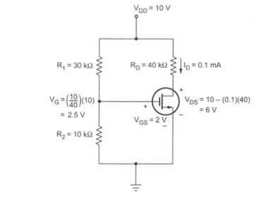
Sol:
VG = VGS = (R2/R1+R2) VDD = (10/10+30) (10) = 2.5V
Assuming that the MOSFET is biased in the saturation region the drain current is
VDS = VDD – ID RD = 10 – (0.1)(40) = 6V.
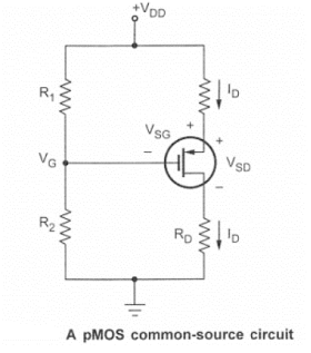
Here, the source is tied to +VDD, Which, become signal ground in the a.c. Equivalent circuit. Thus, it is also a common-source circuit.
The d.c. Analysis for this circuit is essentially the same as for the n-channel MOSFET circuit. The gate voltage is given by,
VG = (R2/R1 + R2) (VDD)
And the source to gate voltage is given by
VSG = VDD -VG
Assuming VGS <VT or VSG > |VT| the device in the saturation region and the drain current is given by
ID = K(VSG + VT) 2
And the source to drain voltage is given by
VSD = VDD – ID RD
If VSD > VSD (sat) then MOSFET is in saturation region.
IF VSD < VSD(sat) MOSFET is in non-saturation region.
Q. For the circuit shown in figure calculate ID , VDS, VG and VS
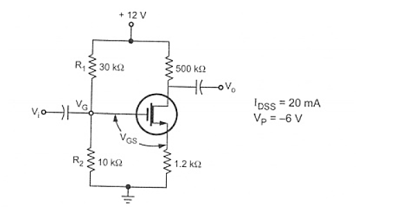
Sol:
Applying KVL to the input circuit.
VGS = VG – VS
= 3 – IS RS Since VS = IS RS
= 3 – ID RS Since ID = IS
We have
ID = IDSS ( 1 – VGS / VP ) 2
Substituting the value of VGS we get
ID = IDSS ( 1 – (3 – ID RS)/Vp) 2 = 20 x 10 -3 ( 1 – ( 3 – ID x 1.2 x 10 3 / -6)
= 20 x 10 -3 ( 1 – [ (-0.5) + 200 ID ]) 2 = 20 x 10 -3 ( 1.5 -2)
= 20 x 10 -3 (2.25 – 600ID + 40000ID 2)
I D = 0.045 – 12 I D + 800 I D 2
800 I D 2 – 13 I D + 0.045 =0
Solving for quadratic equation we get
= -(-13) ± [ (13) 2 – 4(800)(0.045)] ½ / 2(800)
= 13 ± [ 169 -144] ½ / 1600 = 13 ±  / 1600 = 13 ± 5 /1600 = 5mA or 11.25 mA
If we calculate the value of VDS taking ID = 11.25mA we get
VDS = VDD – ID ( RD + RS)
= 12 – 11.25 x 10 -3 ( 500 + 1.2 x 10 3)
= 12 – 19.125 = -7.125
Practically the value of VDS must be positive hence ID= 11.25 mA is invalid
Hence take ID = 5mA
VDS = VDD – ID (RD + RS) = 12 – 5 x 10 -3 (500 + 1.2 x 10 3) = 12 – 8.5 = 3.5 V
VGS = 3 – ID RS = 3- 5 x 10 -3 x 1.2 x 10 3 = 3 – 6 = -3 V
Vs = ID RS = 5 x 10 -3 x 1.2 x 10 3 = 6V
Common source amplifier with Voltage divider bias
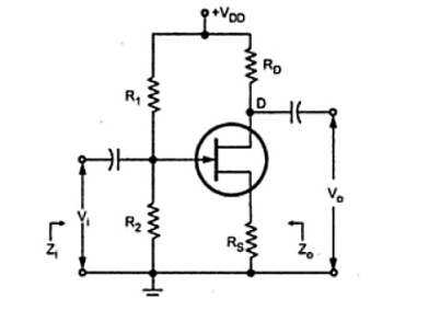
Figure 7. Common Source Amplifier
Now Rs will be the part of low frequency equivalent model as shown in figure.
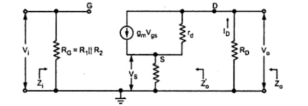
Figure 8. Equivalent model
Note that RG = R1 || R2
Z1 = RG = R1 || R@
Zo’ = rd + gm Rs rd + Rs
Zo’ = rd + Rs ( μ + 1)
Zo = [ rd + gm Rs rd + Rs] || RD
Zo = [ rd + Rs (( μ + 1)] || RD
Av = -gm RD/ 1+ gm Rs + Rs + RD/ rd
In this circuit, input is applied between source and gate and output is taken between drain and gate.
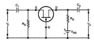
Figure 9. Common Gate Amplifier
In CG Configuration, gate potential is at constant potential. So, increase in input voltage Vi in positive direction increase the negative gate source voltage. Due to ID reduces, reduces, reducing the drop IDRD.
Since VD= VDD-IDRD, the reduction in ID results in an increase in output voltage.
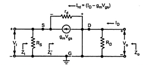
Figure 10. Equivalent model
Input Impedance (Zi)
Zi = Rs || Zi’
And
Zi’ = Vi/I
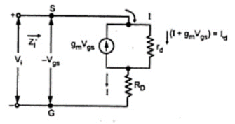
After substituting and simplification,
Vi/I = 1 + RD/rd / 1/rd + gm = rd + RD / 1 + gm rd
Zi = Rs || Zi’ = Rs || rd + RD / 1+gm rd
If rd >> RD and gm rd >> 1 then we can write
Z1 = Rs || rd / gm rd = Rs || 1/gm
Output Impedance

It is given by
Zo = rd || RD
If rd >> RD
Zo = RD
Voltage gain:
Av = Vo/Vi
Vo = - I D R D
Vi = - Vgs
Using KVL to the outer loop after simplication
Av = Vo/ Vi = - Id + RD / -Id ( rd + RD) / 1+ gm rd
If rd >> RD and gmrd >>1
Av = RD (gm rd) / rd = RD gm
In this circuit, input is applied between gate and source and output is taken between source and drain.
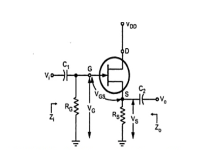
Figure 11. Common Drain Amplifier
In this circuit, the source voltage is
Vs = VG+VGS
When a signal is applied to the JFET gate via C1 ,VG varies with the signal. As VGS is fairly constant and Vs = VG+VGS, Vs varies with Vi.
The following figure shows the low frequency equivalent model for common drain circuit.
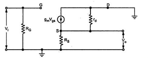
Input Impedance Zi

Zi = RG
Output Impedance Zo
It is given by
Zo = Zo’ || Rs
Where Zo’ = Vo/Id | Vi=0
Applying KVL to the outer loop we have
Vi + Vgs -Vo =0
Vi=0
Looking at the figure we can write
Gm Vgs = Id
But Vgs = Vo
Gm Vo = Id
Zo’ = Vo/Id = 1/gm
Zo = 1/gm || Rs
Voltage gain (Av)
It is given by
Av = Vo/Vi
Looking at the figure we can write
Vo = -Id (rd|| Rs)
And Id = gm Vgs
Vo = -gm Vgs (rd||Rs)
But
Vi = -Vgs + Vo
= - Vgs + [ -gm Vgs (rd||Rs)
Substitute the value Vo and Vi. Then
Av = -gm vgs (rd||Rs) / -Vgs (1+gm (rd||Rs)
= gm (rd||Rs) / 1+gm (rd || Rs)
If rd >> Rs
Av = gm Rs / 1+ gm Rs
If gm Rs >> 1
Av = 1 but it is always less than one.
Common drain circuit does not provide voltage gain.& there is no phase shift between input and output voltages.
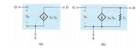
a- Without early affect
b- With early affect
Figure 12. Small signal equivalent circuit
This relationship can be modelled by a current source. Moreover, the gate of the MOSFET is essentially an open circuit at DC. Hence, the small-signal equivalent-circuit model is presented in Figure
When the Early effect has to be accounted for, an output resistor ro can be added as shown in Figure . The value of ro is given as
r o = |VA|/ID where ID = ½ kn V 2 ov
The voltage gain is
Av = vds / vgs = -gm (RD ||ro)
The transconductance is given by
Gm = k’n (W/L) (VGS – Vt) = k’n (W/L) VOV = μ n Cox (W/L) VOV
The transconductance can be increased by increasing the W/L ratio, and also increasing the overdrive voltage VOV. But increasing VOV implies that the operating point for VDS has to increase in order for the MOSFET to be in the saturation region. Also, by using the fact that
ID = ½ Kn V2 OV = ½ k’n (W/L) V2 ov
V ov = [ 2ID / k’n (W/L)] ½
Gm = [ 2 k’n (W/L) I D ] ½
This implies that gm is proportional to the square roots of the drain current ID, and W/L.
High frequency equivalent circuit

Figure 13. High frequency equivalent circuit.
Y = 1/Z = YL + Yds + gd + Ygd
Where
YL = 1/RL ; admittance corresponding to RL
Yds = jw Cds ; admittance corresponding to Cds
Gd = 1/rd ; conductance corresponding to rd
Ygd = jw Cgd ;admittance corresponding to Cgd.
I = -gm Vi + Vi Ygd = Vi(-gm + Ygd)
Voltage gain:
The voltage gain for common source amplifier circuit with load RL is given by
Av = Vo/Vi = IZ/Vi = 1/ViY
Substituting the values of I nd Y we get
AV = -gm + Ygd/ YL + Yds + gd + Ygd
At low frequencies Yds and Ygd =0 hence
Av = -gm +Ygd/YL + gd = -gm rd ZL/ (YL +gd) rd ZL = -gmrdZL/ rd + ZL
= -gm ZL where ZL = rd ||ZL
Input Admittance :
Yi = Ygs + (1-Av) Ygd
Input capacitance
Av = -gm R’d
Substituting the value of Av
Yi/jw = Ci= Cgs +(1+gmR’d) Cgd
This increase in input capacitance Ci over the capacitance from gate to source is called Miller effect.
This input capacitance affects the gain at high frequencies in the operation of cascaded amplifiers.
In cascaded amplifiers, the output from one stage is used as the input to a second amplifier. The input impedance of a second stage acts as a shunt across output of the first stage and Rd is shunted by the capacitance Ci.
Output Admittance:
The output impedance is obtained by looking into the drain with the input voltage set equal to zero. If Vi = 0 in figure, rd , Cds and Cgd in parallel. Hence the output admittance with RL considered external to the amplifier is given by,
Yo = gd + Yds + Ygd
References:
- Op-amps and linear integrated circuit technology Book by Ramakant A. Gayakwad
- Principles of Analog Electronics Textbook by Giovanni Saggio
- Analog electronics Book by Ian Hickman
- Analog Electronics with Op-amps: A Source Book of Practical Circuits Book by Anthony Peyton, V. Walsh, and Y. Walsh