Unit - 3
Combinational Circuits Design
- Half Adder
It is a combinational circuit which has two inputs and two outputs.
It is designed to add two single bit binary number A and B.
It has two outputs carry and sum.
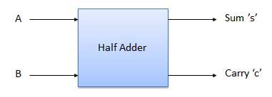
Fig.: Half adder

Fig: Truth Table
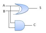
Fig: Circuit Diagram Half adder
Full Adder
- It is developed to overcome the drawback of Half Adder circuit.
- It can add two one-bit numbers A and B and a carry C.
- It is a three input and two output combinational circuit.

Fig: Block diagram Full adder

Fig: Truth Table

Fig: Circuit Diagram Full adder
Key Takeaways:
- Half adder is a combinational circuit which has two inputs and two outputs.
- Since there is no provision for carry in half adder, full adder is developed to overcome the drawback.
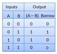
- Half Subtractors
It is a combination circuit with two inputs and two outputs.
The difference between the two binary bits is obtained at the output and an output (Borrow) indicates if a 1 has been borrowed.
Here A is called as Minuend bit and B is called as Subtrahend bit.
Truth Table

Circuit Diagram
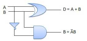
Half subtractor
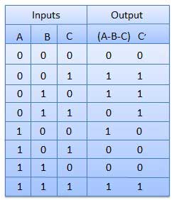
B. Full Subtractors
It is a combinational circuit which has three inputs A, B, C and two output D and C'.
A is the 'minuend', B is 'subtrahend', C is the 'borrow' which is produced by the previous stage, difference output D and C' is the borrow output.
Truth Table

Circuit Diagram
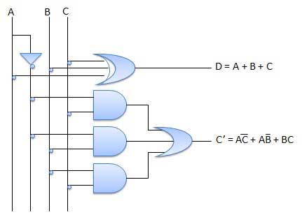
Full subtractor
Key Takeaways:
- Half subtractor is a combinational circuit which has two inputs and two outputs.
- Since there is no provision for borrow in half subtractor, full subtractor is developed to overcome the drawback.
A single full adder performs the addition of two one bit numbers and an input carry. But a Parallel Adder is a digital circuit capable of finding the arithmetic sum of two binary numbers that is greater than one bit in length by operating on corresponding pairs of bits in parallel. It consists of full adders connected in a chain where the output carry from each full adder is connected to the carry input of the next higher order full adder in the chain. A n bit parallel adder requires n full adders to perform the operation. So for the two-bit number, two adders are needed while for four bit number, four adders are needed and so on. Parallel adders normally incorporate carry lookahead logic to ensure that carry propagation between subsequent stages of addition does not limit addition speed.

Figure: Parallel adder
Working:
- As shown in the figure, firstly the full adder FA1 adds A1 and B1 along with the carry C1 to generate the sum S1 (the first bit of the output sum) and the carry C2 which is connected to the next adder in chain.
- Next, the full adder FA2 uses this carry bit C2 to add with the input bits A2 and B2 to generate the sum S2(the second bit of the output sum) and the carry C3 which is again further connected to the next adder in chain and so on.
- The process continues till the last full adder FAn uses the carry bit Cn to add with its input An and Bn to generate the last bit of the output along last carry bit Cout.
BCD stands for binary coded decimal.
Suppose, we have two 4-bit numbers A and B. The value of A and B can vary from 0(0000 in binary) to 9(1001 in binary).
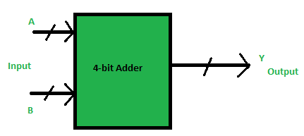
Fig.: BCD adder
- The output varies from 0 to 18 if the carry from the previous sum is not considered.
- But if we consider the carry, then the maximum value of output will be 19 (i.e., 9+9+1 = 19).
- When we simply add A and B, then we get the binary sum, and to get the output in BCD form, we use BCD Adder.
Example 1:
Input:
A = 0111 B = 1000
Output:
Y = 1 0101
Explanation: We are adding A (=7) and B (=8).
The value of the binary sum will be 1111(=15).
But the BCD sum will be 1 0101,
Where 1 is 0001 in binary and 5 is 0101 in binary.
Example 2:
Input:
A = 0101 B = 1001
Output:
Y = 1 0100
Explanation: We are adding A (=5) and B (=9).
The value of the binary sum will be 1110(=14).
But the BCD sum will be 1 0100,
Where 1 is 0001 in binary and 4 is 0100 in binary.
Now, let's move to the table and find out the logic when we are going to add “0110”.
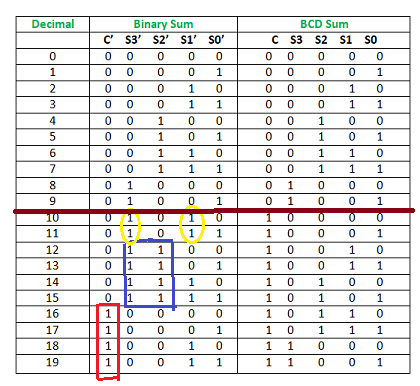
Fig.: Table explaining BCD addition (ref. 2)
We are adding “0110” (=6) only to the second half of the table because of the following conditions:
- If C’ = 1 (Satisfies 16-19)
- If S3′. S2′ = 1 (Satisfies 12-15)
- If S3′. S1′ = 1 (Satisfies 10 and 11)
So, our logic is
C' + S3’. S2' + S3’. S1' = 1
Implementation:

Fig.: BCD adder (ref. 2)
A binary multiplier is a combinational logic circuit or digital device used for multiplying two binary numbers. The two numbers are more specifically known as multiplicand and multiplier and the result is known as a product.
The multiplicand & multiplier can be of various bit size. The product’s bit size depends on the bit size of the multiplicand & multiplier. The bit size of the product is equal to the sum of the bit size of multiplier & multiplicand.
Binary multiplication method is same as decimal multiplication. Binary multiplication of more than 1-bit numbers contains 2 steps. The 1st step is single bit-wise multiplication known as partial product and the 2nd step is adding all partial products into a single product.
Partial products or single bit products can be obtained by using AND gates. However, to add these partial products we need full adders & half adders.
The schematic design of a digital multiplier differs with bit size. The design becomes complex with the increase in bit size of the multiplier.
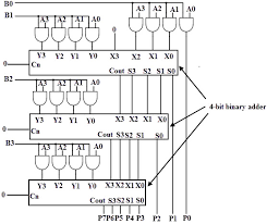
Figure: Binary Multiplier
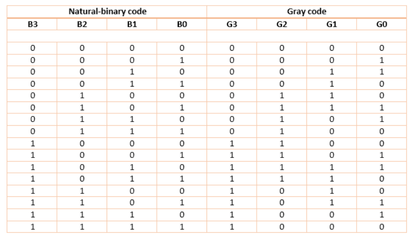
Binary To Gray Code

For this circuit, B3 B2 B1 B0 are inputs while G3 G2 G1 G0 are outputs.
K-map for the outputs:
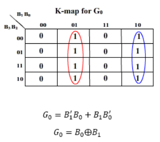
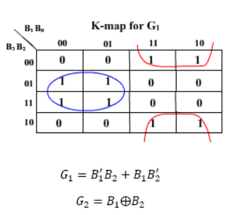
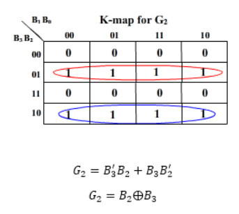
And G3 = B3
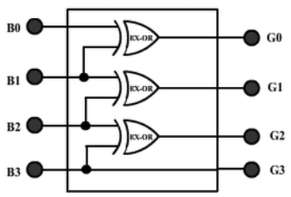
2. Gray to Binary Code

Then the K-maps:

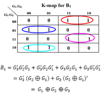
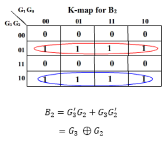
And B3 = G3
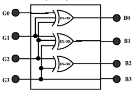
The realization of Gray-to-Binary converter is

Key Takeaways:
- These are the combinational circuits made by conversion of one code to another.
- The parity generating technique is used as error detection technique for the data transmission.
- When binary data is transmitted and processed, it is subjected to noise and that noise can alter 0s to 1s and 1s to 0s of data bits in digital systems.
- Therefore, a parity generator is a combinational logic circuit that generates the parity bit at the transmitter end.
- The basic principle is that sum of odd number of 1s is always 1 and sum of even number of 1s is always zero.
- Such error detection and correction can be implemented by using Ex-OR gates.
Even Parity Generator
A 3-bit message is transmitted with an even parity bit. Hence assuming, the three inputs W, X and Y that are applied to the circuits and output bit is the parity bit P. The total number of 1s must be even, to generate the even parity bit P.
3- bit message | Even Parity | ||
W | X | Y | P |
0 | 0 | 0 | 0 |
0 | 0 | 1 | 1 |
0 | 1 | 0 | 1 |
0 | 1 | 1 | 0 |
1 | 0 | 0 | 1 |
1 | 0 | 1 | 0 |
1 | 1 | 0 | 0 |
1 | 1 | 1 | 1 |
The K-map simplification for 3-bit message even parity generator is
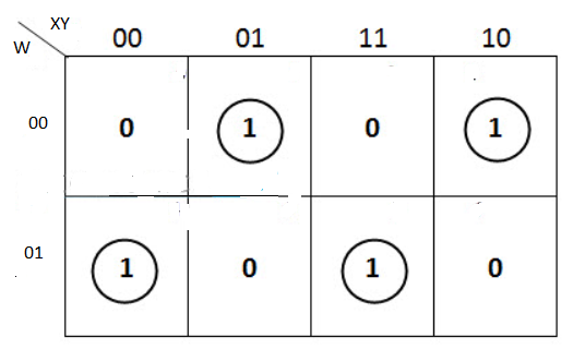
From the above K-Map, the expression is:
P=W′X′Y+W′XY′+WX′Y′+WXY
P=W′(X′Y+XY′) +W(X′Y′+XY)
P=W′(X⊕Y) +W(X⊕Y) ′=W⊕X⊕Y

Odd Parity Generator
Considering that the 3-bit data is transmitted with an odd parity bit. The three inputs are W, X and Y and P is the output parity bit. The total number of bits must be odd in order to generate the odd parity bit.
3- bit message | Odd Parity | ||
W | X | Y | P |
0 | 0 | 0 | 1 |
0 | 0 | 1 | 0 |
0 | 1 | 0 | 0 |
0 | 1 | 1 | 1 |
1 | 0 | 0 | 0 |
1 | 0 | 1 | 1 |
1 | 1 | 0 | 1 |
1 | 1 | 1 | 0 |
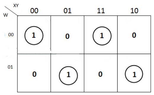
The K-map simplification for 3-bit message even parity generator is

A comparator is a logic circuit, used to compare the magnitude of two binary numbers.
The following figure shows the block diagram of a n-bit comparator.

Fig.: Comparator
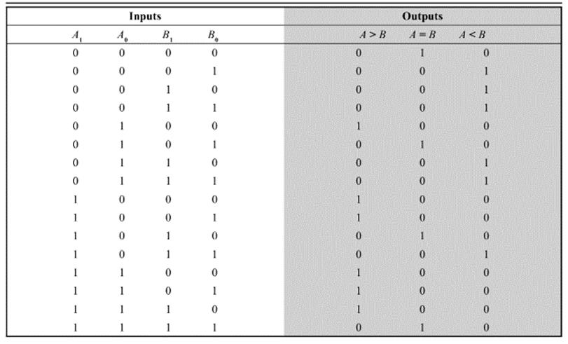
It receives two n-bit numbers A and B as inputs and the outputs are A>B, A=B and A<B. Depending upon the relative magnitude of the two numbers, one of the outputs will be high.
The following is the truth table of a 2-bit comparator.
- It works as an inverse of an encoder.
- It is a combinational circuit which converts n input lines into 2n output lines.
- Taking an example of 3-to-8-line decoder.
Truth Table –
X | Y | Z | D0 | D1 | D2 | D3 | D4 | D5 | D6 | D7 |
0 | 0 | 0 | 1 | 0 | 0 | 0 | 0 | 0 | 0 | 0 |
0 | 0 | 1 | 0 | 1 | 0 | 0 | 0 | 0 | 0 | 0 |
0 | 1 | 0 | 0 | 0 | 1 | 0 | 0 | 0 | 0 | 0 |
0 | 1 | 1 | 0 | 0 | 0 | 1 | 0 | 0 | 0 | 0 |
1 | 0 | 0 | 0 | 0 | 0 | 0 | 1 | 0 | 0 | 0 |
1 | 0 | 1 | 0 | 0 | 0 | 0 | 0 | 1 | 0 | 0 |
1 | 1 | 0 | 0 | 0 | 0 | 0 | 0 | 0 | 1 | 0 |
1 | 1 | 1 | 0 | 0 | 0 | 0 | 0 | 0 | 0 | 1 |
Implementation
D0 is high when X = 0, Y = 0 and Z = 0. Hence,
D0 = X’ Y’ Z’
Similarly,
D1 = X’ Y’ Z
D2 = X’ Y Z’
D3 = X’ Y Z
D4 = X Y’ Z’
D5 = X Y’ Z
D6 = X Y Z’
D7 = X Y Z
Hence,

Fig: Decoder
Key Takeaways:
- It works as an inverse of an encoder.
- It is a combinational circuit which converts n input lines into 2n output lines.
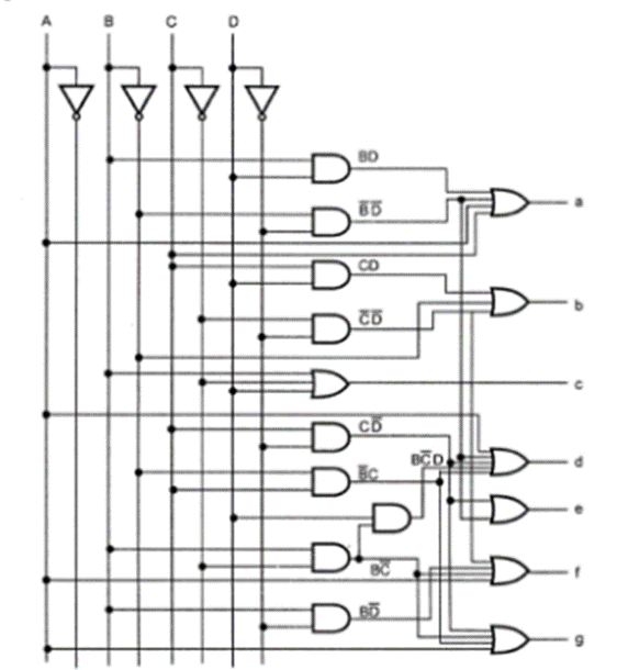
In most practical applications, seven segment displays are used to give a visual indication of the output states of digital IC’s such a decade counters, latches etc. For using this display device, the data has to be converted from some binary code to the code required for the display. Usually, the binary code used is natural BCD.
The following figure shows the display device and the segments which must be illuminated for each of the numerals.

The display system can be connected as follows:

Here, ABCD is the natural BCD code for numerals 0 through 9. Following is the truth table of BCD to 7-segment decoder
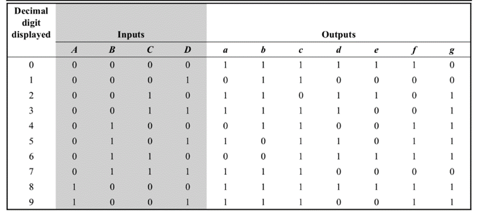
The K-Maps for each of the outputs A through G are given below:
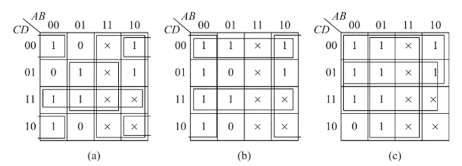
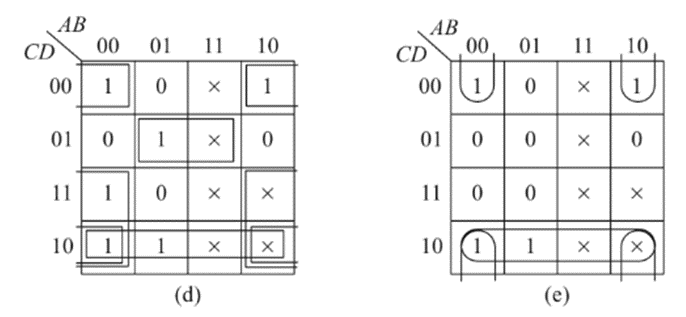

The simplified expressions obtained from the k-maps are:
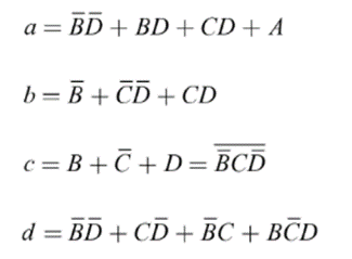
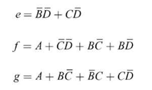
Logic diagram:
- Binary code of N digits is used to store 2N distinct elements of coded information.
- This is the reason why encoders and decoders are used.
- Encoders convert 2N lines of input into a code of N bits and Decoders decode those N bits into 2N lines.
Encoders –
- It is a combinational circuit that converts binary information in the form of a 2N input lines into N output lines, which represent N bit code for the input.
- For simple encoders, only one input line is active at a time.
- For example: Octal to Binary encoder takes 8 input lines and generates 3 output lines.
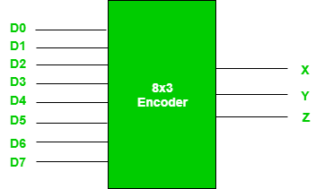
Fig.: 8X3 Encoder
Truth Table –
D7 | D6 | D5 | D4 | D3 | D2 | D1 | D0 | X | Y | Z |
0 | 0 | 0 | 0 | 0 | 0 | 0 | 1 | 0 | 0 | 0 |
0 | 0 | 0 | 0 | 0 | 0 | 1 | 0 | 0 | 0 | 1 |
0 | 0 | 0 | 0 | 0 | 1 | 0 | 0 | 0 | 1 | 0 |
0 | 0 | 0 | 0 | 1 | 0 | 0 | 0 | 0 | 1 | 1 |
0 | 0 | 0 | 1 | 0 | 0 | 0 | 0 | 1 | 0 | 0 |
0 | 0 | 1 | 0 | 0 | 0 | 0 | 0 | 1 | 0 | 1 |
0 | 1 | 0 | 0 | 0 | 0 | 0 | 0 | 1 | 1 | 0 |
1 | 0 | 0 | 0 | 0 | 0 | 0 | 0 | 1 | 1 | 1 |
- From the above truth table, it is seen that the output is 000 when D0 is active; 001 when D1 is active; 010 when D2 is active and so on.
Implementation –
- From the above truth table, the output Z is active when the input octal digit is 1, 3, 5 or 7.
- Y is active when input octal digit is 2, 3, 6 or 7 and X is active when input octal digits 4, 5, 6 or 7.
- Hence, the Boolean functions would be:
X = D4 + D5 + D6 + D7
Y = D2 +D3 + D6 + D7
Z = D1 + D3 + D5 + D7
- Hence, the encoder is realized with OR gates as follows:
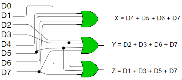
Fig: 8:3 encoder
- Limitation of the encoder is that only one input is active at a time.
- If more than one input is active, then the output of encoder is undefined.
- For example, if D6 and D3 are both active, then, our output would be 111 which is the output for D7.
- Problem arises when all inputs are 0.
- The encoder gives output 000 which actually is the output for D0. To avoid this, an extra bit is added to the output which is called the valid bit whose value is 0 when all inputs are 0 or 1.
- It is an encoder whose inputs are given priorities.
- When more than one input becomes active at the same time then the input with higher priority takes precedence w.r.to the output which is generated.
- Considering a 4:2 priority encoder.
- From the truth table given below we see that when all inputs are 0, V bit is zero and outputs are not used.
- The x in the table shows the don’t care condition, i.e. it can be 0 or 1.
- Here, D3 has highest priority, therefore, when D3 is high, output has to be 11.
- D0 has the lowest priority, hence the output would be 00 only when D0 is high and all the other input lines are low.
Truth Table –
D3 | D2 | D1 | D0 | X | Y | V |
0 | 0 | 0 | 0 | x | x | 0 |
0 | 0 | 0 | 1 | 0 | 0 | 1 |
0 | 0 | 1 | x | 0 | 1 | 1 |
0 | 1 | X | x | 1 | 0 | 1 |
1 | x | X | x | 1 | 1 | 1 |
Implementation
The condition for valid bit to be 1 is when at least one of the inputs should be high. Hence,
V = D0 + D1 + D2 + D3
For X:
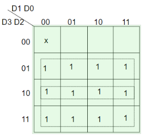
=>X=D2+D3
For Y:

=> Y = D1 D2’ + D3
Hence, the priority 4-to-2 encoder can be realized as follows:

Fig: Priority encoder
Key takeaway
An Encoder is a combinational circuit that performs the reverse operation of Decoder. It has maximum of 2n input lines and ‘n’ output lines. It will produce a binary code equivalent to the input, which is active High.
- It is a special type of combinational circuit.
- It has n-data inputs, one output and m inputs select lines with 2m = n.
- It selects one of the n data inputs and routes it to the output.
- The selection of one of the inputs is done by the select lines.
- Depending on the code applied at the inputs, one of the n data sources is selected and transmitted to the single output Y.
- E is the enable input which is useful for cascading purpose.
- It is an active low terminal hence performs the required operation when it is low.
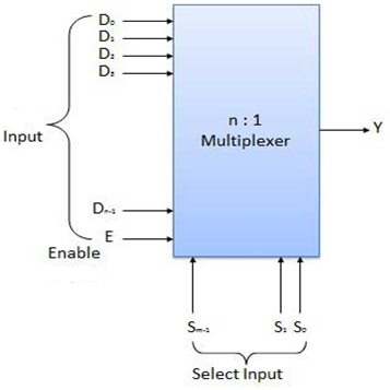
Fig.: Block diagram of multiplexer
Multiplexers come in multiple variations
- 2: 1 multiplexer
- 4: 1 multiplexer
- 16: 1 multiplexer
- 32: 1 multiplexer
Block Diagram of 2:1 MUX
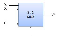
Fig.: 2:1 MUX
Truth Table of 2:1 MUX
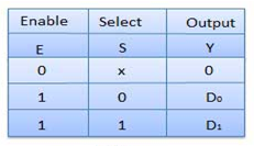
Where x is don’t care.
Key Takeaways
- It has n-data inputs, one output and m inputs select lines with 2m = n.
- The selection of one of the inputs is done by the select lines.
- It performs the inverse operation of a multiplexer as it receives one input and distributes it across its outputs.
- It has only one input and n outputs with m select input.
- At a time only one output line is selected by the select lines and that input is transmitted through the output line.
- It is equivalent to a single pole multiple way switch.
Various Demultiplexers are used as:
- 1: 2 demultiplexer
- 1: 4 demultiplexer
- 1: 16 demultiplexer
- 1: 32 demultiplexer
Block diagram

Truth Table

Where x is don’t care.
Key Takeaways:
- It performs the inverse operation of a multiplexer as it receives one input and distributes it across its outputs.
- It has only one input and n outputs with m select input.
References:
1. Rajkamal ‘Digital Systems Principals and Design’ Pearson Education
2. A.P. Malvino, D.P. Leach ‘Digital Principles & Applications’ -VIth Edition-TMH publication.
3. M. Morris Mano ‘Digital Design’ (Third Edition). PHI Publications
Unit - 3
Combinational Circuits Design
Unit - 3
Combinational Circuits Design
Unit - 3
Combinational Circuits Design
- Half Adder
It is a combinational circuit which has two inputs and two outputs.
It is designed to add two single bit binary number A and B.
It has two outputs carry and sum.

Fig.: Half adder
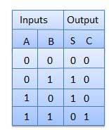
Fig: Truth Table

Fig: Circuit Diagram Half adder
Full Adder
- It is developed to overcome the drawback of Half Adder circuit.
- It can add two one-bit numbers A and B and a carry C.
- It is a three input and two output combinational circuit.
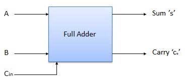
Fig: Block diagram Full adder
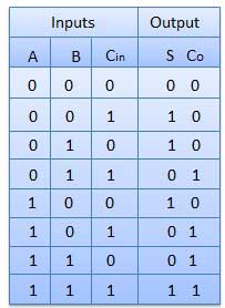
Fig: Truth Table
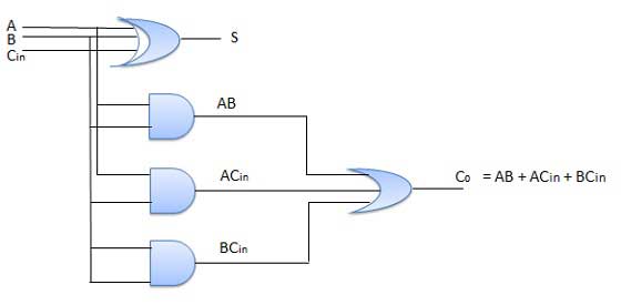
Fig: Circuit Diagram Full adder
Key Takeaways:
- Half adder is a combinational circuit which has two inputs and two outputs.
- Since there is no provision for carry in half adder, full adder is developed to overcome the drawback.
- Half Subtractors
It is a combination circuit with two inputs and two outputs.
The difference between the two binary bits is obtained at the output and an output (Borrow) indicates if a 1 has been borrowed.
Here A is called as Minuend bit and B is called as Subtrahend bit.
Truth Table
Circuit Diagram

Half subtractor
B. Full Subtractors
It is a combinational circuit which has three inputs A, B, C and two output D and C'.
A is the 'minuend', B is 'subtrahend', C is the 'borrow' which is produced by the previous stage, difference output D and C' is the borrow output.
Truth Table
Circuit Diagram

Full subtractor
Key Takeaways:
- Half subtractor is a combinational circuit which has two inputs and two outputs.
- Since there is no provision for borrow in half subtractor, full subtractor is developed to overcome the drawback.
A single full adder performs the addition of two one bit numbers and an input carry. But a Parallel Adder is a digital circuit capable of finding the arithmetic sum of two binary numbers that is greater than one bit in length by operating on corresponding pairs of bits in parallel. It consists of full adders connected in a chain where the output carry from each full adder is connected to the carry input of the next higher order full adder in the chain. A n bit parallel adder requires n full adders to perform the operation. So for the two-bit number, two adders are needed while for four bit number, four adders are needed and so on. Parallel adders normally incorporate carry lookahead logic to ensure that carry propagation between subsequent stages of addition does not limit addition speed.

Figure: Parallel adder
Working:
- As shown in the figure, firstly the full adder FA1 adds A1 and B1 along with the carry C1 to generate the sum S1 (the first bit of the output sum) and the carry C2 which is connected to the next adder in chain.
- Next, the full adder FA2 uses this carry bit C2 to add with the input bits A2 and B2 to generate the sum S2(the second bit of the output sum) and the carry C3 which is again further connected to the next adder in chain and so on.
- The process continues till the last full adder FAn uses the carry bit Cn to add with its input An and Bn to generate the last bit of the output along last carry bit Cout.
BCD stands for binary coded decimal.
Suppose, we have two 4-bit numbers A and B. The value of A and B can vary from 0(0000 in binary) to 9(1001 in binary).

Fig.: BCD adder
- The output varies from 0 to 18 if the carry from the previous sum is not considered.
- But if we consider the carry, then the maximum value of output will be 19 (i.e., 9+9+1 = 19).
- When we simply add A and B, then we get the binary sum, and to get the output in BCD form, we use BCD Adder.
Example 1:
Input:
A = 0111 B = 1000
Output:
Y = 1 0101
Explanation: We are adding A (=7) and B (=8).
The value of the binary sum will be 1111(=15).
But the BCD sum will be 1 0101,
Where 1 is 0001 in binary and 5 is 0101 in binary.
Example 2:
Input:
A = 0101 B = 1001
Output:
Y = 1 0100
Explanation: We are adding A (=5) and B (=9).
The value of the binary sum will be 1110(=14).
But the BCD sum will be 1 0100,
Where 1 is 0001 in binary and 4 is 0100 in binary.
Now, let's move to the table and find out the logic when we are going to add “0110”.

Fig.: Table explaining BCD addition (ref. 2)
We are adding “0110” (=6) only to the second half of the table because of the following conditions:
- If C’ = 1 (Satisfies 16-19)
- If S3′. S2′ = 1 (Satisfies 12-15)
- If S3′. S1′ = 1 (Satisfies 10 and 11)
So, our logic is
C' + S3’. S2' + S3’. S1' = 1
Implementation:
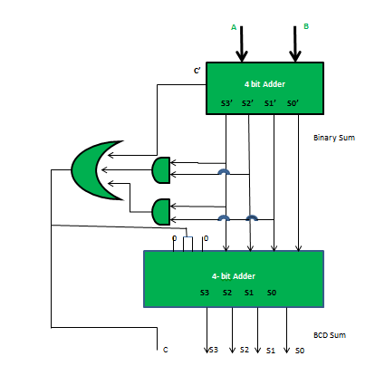
Fig.: BCD adder (ref. 2)
A binary multiplier is a combinational logic circuit or digital device used for multiplying two binary numbers. The two numbers are more specifically known as multiplicand and multiplier and the result is known as a product.
The multiplicand & multiplier can be of various bit size. The product’s bit size depends on the bit size of the multiplicand & multiplier. The bit size of the product is equal to the sum of the bit size of multiplier & multiplicand.
Binary multiplication method is same as decimal multiplication. Binary multiplication of more than 1-bit numbers contains 2 steps. The 1st step is single bit-wise multiplication known as partial product and the 2nd step is adding all partial products into a single product.
Partial products or single bit products can be obtained by using AND gates. However, to add these partial products we need full adders & half adders.
The schematic design of a digital multiplier differs with bit size. The design becomes complex with the increase in bit size of the multiplier.

Figure: Binary Multiplier
Binary To Gray Code
For this circuit, B3 B2 B1 B0 are inputs while G3 G2 G1 G0 are outputs.
K-map for the outputs:


And G3 = B3

2. Gray to Binary Code
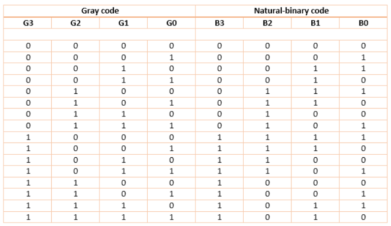
Then the K-maps:
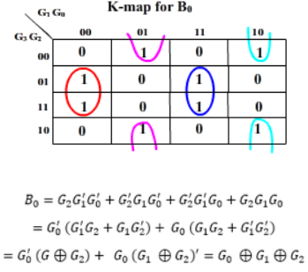


And B3 = G3
The realization of Gray-to-Binary converter is
Key Takeaways:
- These are the combinational circuits made by conversion of one code to another.
- The parity generating technique is used as error detection technique for the data transmission.
- When binary data is transmitted and processed, it is subjected to noise and that noise can alter 0s to 1s and 1s to 0s of data bits in digital systems.
- Therefore, a parity generator is a combinational logic circuit that generates the parity bit at the transmitter end.
- The basic principle is that sum of odd number of 1s is always 1 and sum of even number of 1s is always zero.
- Such error detection and correction can be implemented by using Ex-OR gates.
Even Parity Generator
A 3-bit message is transmitted with an even parity bit. Hence assuming, the three inputs W, X and Y that are applied to the circuits and output bit is the parity bit P. The total number of 1s must be even, to generate the even parity bit P.
3- bit message | Even Parity | ||
W | X | Y | P |
0 | 0 | 0 | 0 |
0 | 0 | 1 | 1 |
0 | 1 | 0 | 1 |
0 | 1 | 1 | 0 |
1 | 0 | 0 | 1 |
1 | 0 | 1 | 0 |
1 | 1 | 0 | 0 |
1 | 1 | 1 | 1 |
The K-map simplification for 3-bit message even parity generator is

From the above K-Map, the expression is:
P=W′X′Y+W′XY′+WX′Y′+WXY
P=W′(X′Y+XY′) +W(X′Y′+XY)
P=W′(X⊕Y) +W(X⊕Y) ′=W⊕X⊕Y

Odd Parity Generator
Considering that the 3-bit data is transmitted with an odd parity bit. The three inputs are W, X and Y and P is the output parity bit. The total number of bits must be odd in order to generate the odd parity bit.
3- bit message | Odd Parity | ||
W | X | Y | P |
0 | 0 | 0 | 1 |
0 | 0 | 1 | 0 |
0 | 1 | 0 | 0 |
0 | 1 | 1 | 1 |
1 | 0 | 0 | 0 |
1 | 0 | 1 | 1 |
1 | 1 | 0 | 1 |
1 | 1 | 1 | 0 |
The K-map simplification for 3-bit message even parity generator is


A comparator is a logic circuit, used to compare the magnitude of two binary numbers.
The following figure shows the block diagram of a n-bit comparator.
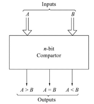
Fig.: Comparator
It receives two n-bit numbers A and B as inputs and the outputs are A>B, A=B and A<B. Depending upon the relative magnitude of the two numbers, one of the outputs will be high.
The following is the truth table of a 2-bit comparator.

- It works as an inverse of an encoder.
- It is a combinational circuit which converts n input lines into 2n output lines.
- Taking an example of 3-to-8-line decoder.
Truth Table –
X | Y | Z | D0 | D1 | D2 | D3 | D4 | D5 | D6 | D7 |
0 | 0 | 0 | 1 | 0 | 0 | 0 | 0 | 0 | 0 | 0 |
0 | 0 | 1 | 0 | 1 | 0 | 0 | 0 | 0 | 0 | 0 |
0 | 1 | 0 | 0 | 0 | 1 | 0 | 0 | 0 | 0 | 0 |
0 | 1 | 1 | 0 | 0 | 0 | 1 | 0 | 0 | 0 | 0 |
1 | 0 | 0 | 0 | 0 | 0 | 0 | 1 | 0 | 0 | 0 |
1 | 0 | 1 | 0 | 0 | 0 | 0 | 0 | 1 | 0 | 0 |
1 | 1 | 0 | 0 | 0 | 0 | 0 | 0 | 0 | 1 | 0 |
1 | 1 | 1 | 0 | 0 | 0 | 0 | 0 | 0 | 0 | 1 |
Implementation
D0 is high when X = 0, Y = 0 and Z = 0. Hence,
D0 = X’ Y’ Z’
Similarly,
D1 = X’ Y’ Z
D2 = X’ Y Z’
D3 = X’ Y Z
D4 = X Y’ Z’
D5 = X Y’ Z
D6 = X Y Z’
D7 = X Y Z
Hence,
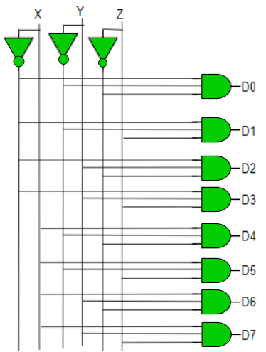
Fig: Decoder
Key Takeaways:
- It works as an inverse of an encoder.
- It is a combinational circuit which converts n input lines into 2n output lines.
In most practical applications, seven segment displays are used to give a visual indication of the output states of digital IC’s such a decade counters, latches etc. For using this display device, the data has to be converted from some binary code to the code required for the display. Usually, the binary code used is natural BCD.
The following figure shows the display device and the segments which must be illuminated for each of the numerals.

The display system can be connected as follows:
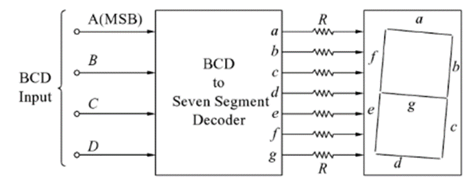
Here, ABCD is the natural BCD code for numerals 0 through 9. Following is the truth table of BCD to 7-segment decoder

The K-Maps for each of the outputs A through G are given below:


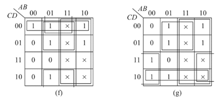
The simplified expressions obtained from the k-maps are:


Logic diagram:

- Binary code of N digits is used to store 2N distinct elements of coded information.
- This is the reason why encoders and decoders are used.
- Encoders convert 2N lines of input into a code of N bits and Decoders decode those N bits into 2N lines.
Encoders –
- It is a combinational circuit that converts binary information in the form of a 2N input lines into N output lines, which represent N bit code for the input.
- For simple encoders, only one input line is active at a time.
- For example: Octal to Binary encoder takes 8 input lines and generates 3 output lines.

Fig.: 8X3 Encoder
Truth Table –
D7 | D6 | D5 | D4 | D3 | D2 | D1 | D0 | X | Y | Z |
0 | 0 | 0 | 0 | 0 | 0 | 0 | 1 | 0 | 0 | 0 |
0 | 0 | 0 | 0 | 0 | 0 | 1 | 0 | 0 | 0 | 1 |
0 | 0 | 0 | 0 | 0 | 1 | 0 | 0 | 0 | 1 | 0 |
0 | 0 | 0 | 0 | 1 | 0 | 0 | 0 | 0 | 1 | 1 |
0 | 0 | 0 | 1 | 0 | 0 | 0 | 0 | 1 | 0 | 0 |
0 | 0 | 1 | 0 | 0 | 0 | 0 | 0 | 1 | 0 | 1 |
0 | 1 | 0 | 0 | 0 | 0 | 0 | 0 | 1 | 1 | 0 |
1 | 0 | 0 | 0 | 0 | 0 | 0 | 0 | 1 | 1 | 1 |
- From the above truth table, it is seen that the output is 000 when D0 is active; 001 when D1 is active; 010 when D2 is active and so on.
Implementation –
- From the above truth table, the output Z is active when the input octal digit is 1, 3, 5 or 7.
- Y is active when input octal digit is 2, 3, 6 or 7 and X is active when input octal digits 4, 5, 6 or 7.
- Hence, the Boolean functions would be:
X = D4 + D5 + D6 + D7
Y = D2 +D3 + D6 + D7
Z = D1 + D3 + D5 + D7
- Hence, the encoder is realized with OR gates as follows:

Fig: 8:3 encoder
- Limitation of the encoder is that only one input is active at a time.
- If more than one input is active, then the output of encoder is undefined.
- For example, if D6 and D3 are both active, then, our output would be 111 which is the output for D7.
- Problem arises when all inputs are 0.
- The encoder gives output 000 which actually is the output for D0. To avoid this, an extra bit is added to the output which is called the valid bit whose value is 0 when all inputs are 0 or 1.
- It is an encoder whose inputs are given priorities.
- When more than one input becomes active at the same time then the input with higher priority takes precedence w.r.to the output which is generated.
- Considering a 4:2 priority encoder.
- From the truth table given below we see that when all inputs are 0, V bit is zero and outputs are not used.
- The x in the table shows the don’t care condition, i.e. it can be 0 or 1.
- Here, D3 has highest priority, therefore, when D3 is high, output has to be 11.
- D0 has the lowest priority, hence the output would be 00 only when D0 is high and all the other input lines are low.
Truth Table –
D3 | D2 | D1 | D0 | X | Y | V |
0 | 0 | 0 | 0 | x | x | 0 |
0 | 0 | 0 | 1 | 0 | 0 | 1 |
0 | 0 | 1 | x | 0 | 1 | 1 |
0 | 1 | X | x | 1 | 0 | 1 |
1 | x | X | x | 1 | 1 | 1 |
Implementation
The condition for valid bit to be 1 is when at least one of the inputs should be high. Hence,
V = D0 + D1 + D2 + D3
For X:

=>X=D2+D3
For Y:
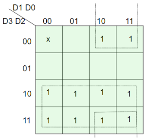
=> Y = D1 D2’ + D3
Hence, the priority 4-to-2 encoder can be realized as follows:
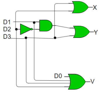
Fig: Priority encoder
Key takeaway
An Encoder is a combinational circuit that performs the reverse operation of Decoder. It has maximum of 2n input lines and ‘n’ output lines. It will produce a binary code equivalent to the input, which is active High.
- It is a special type of combinational circuit.
- It has n-data inputs, one output and m inputs select lines with 2m = n.
- It selects one of the n data inputs and routes it to the output.
- The selection of one of the inputs is done by the select lines.
- Depending on the code applied at the inputs, one of the n data sources is selected and transmitted to the single output Y.
- E is the enable input which is useful for cascading purpose.
- It is an active low terminal hence performs the required operation when it is low.

Fig.: Block diagram of multiplexer
Multiplexers come in multiple variations
- 2: 1 multiplexer
- 4: 1 multiplexer
- 16: 1 multiplexer
- 32: 1 multiplexer
Block Diagram of 2:1 MUX

Fig.: 2:1 MUX
Truth Table of 2:1 MUX

Where x is don’t care.
Key Takeaways
- It has n-data inputs, one output and m inputs select lines with 2m = n.
- The selection of one of the inputs is done by the select lines.
- It performs the inverse operation of a multiplexer as it receives one input and distributes it across its outputs.
- It has only one input and n outputs with m select input.
- At a time only one output line is selected by the select lines and that input is transmitted through the output line.
- It is equivalent to a single pole multiple way switch.
Various Demultiplexers are used as:
- 1: 2 demultiplexer
- 1: 4 demultiplexer
- 1: 16 demultiplexer
- 1: 32 demultiplexer
Block diagram
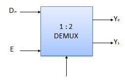
Truth Table
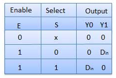
Where x is don’t care.
Key Takeaways:
- It performs the inverse operation of a multiplexer as it receives one input and distributes it across its outputs.
- It has only one input and n outputs with m select input.
References:
1. Rajkamal ‘Digital Systems Principals and Design’ Pearson Education
2. A.P. Malvino, D.P. Leach ‘Digital Principles & Applications’ -VIth Edition-TMH publication.
3. M. Morris Mano ‘Digital Design’ (Third Edition). PHI Publications