Unit – 1
Fundamentals of Microprocessors
- It is a controlling unit that is fabricated on a small chip.
- It is capable to perform arithmetic logic operations and communicate with various devices connected to it.
- It comprises of an ALU (Arithmetic Logic Unit), MU (Memory unit) and CU (Control unit).
- It also consists of register array with registers named as B, C, D, E, H, L and ACC.
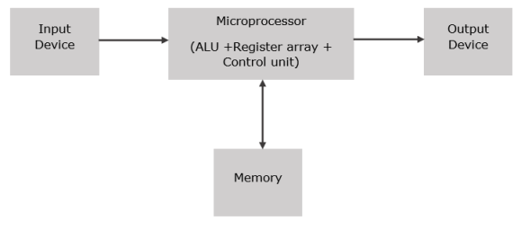
Fig.1: Basic block diagram of microprocessor
Basic functions of microprocessor
- Accumulator
It is an 8-bit register used for performing all arithmetical and logical operations. It is also used to load and store data.
- Arithmetic and logic unit
It performs all arithmetical and logical operations like add, subtract, AND, OR etc.
- General purpose register
There are 6 General purpose registers and they are B, C, D, E, H and L. Each of them can hold 8 bit of data. They can also work in pair known as register pairs and they are H-L, B-C and D-E.
- Program counter (PC)
It is a 16 bit register. It is used to store data, memory information etc. whenever memory is incremented, the PC then points to the next location.
- Stack pointer (SP)
It is a 16 bit register. It always points to stack which can be incremented or decremented by PUSH and POP instruction.
- Temporary register
It is an 8 bit register which is used to store temporary information of the ALU.
- Flag register
It is an 8 bit register.

Here, Sign (S), Zero (Z), Auxiliary Carry (AC), Parity (P),Carry (C) bit.
- Instruction register and decoder
It is an 8-bit register. It stores an instruction that is fetched from memory. It decodes the information present inside it.
- Timing and control unit
It provides timing and control signal to the microprocessor to perform various operations. Following are the signals that controls the external and internal circuits are:
Control Signals: READY, RD’, WR’, ALE
Status Signals: S0, S1, IO/M’
DMA Signals: HOLD, HLDA
RESET Signals: RESET IN, RESET OUT D7
- Interrupt control
It controls the interrupts during a process. When a microprocessor is executing a main program and if an interrupt occurs, the microprocessor shifts the control from the main program to process the incoming request. After the request is completed, the control goes back to the main program.
There are 5 types of interrupts: INTR, RST 7.5, RST 6.5, RST 5.5 and TRAP.
- Serial input/output control
It controls the serial data communication in the microprocessor by using two instructions namely SID (Serial input data) and SOD (Serial output data).
- Address and data bus
Data bus carries the data required to be stored. It is bidirectional. Address bus carries the location to where the data should be stored and it is unidirectional. It is used to transfer the data & address.
System Bus
The system bus comprises of two types of bus:
Address bus
It is a 16-bit bus in which A15-A8, it carries the most significant 8-bits of memory/IO address and AD7-AD0 are multiplexed with data lines that carries the least significant bits of the address.
Data bus
It is an 8-bit bus which is multiplexed with the address lines AD7-AD0. It carries data and also the least significant 8-bit address.
Architecture of 8085
- It includes the timing & control unit, Arithmetic and logic unit, decoder, instruction register, interrupt control, a register array, serial input/output control and the central processing unit.
Operations of 8085 Microprocessor
It performs all arithmetical and logical operations like add, subtract, AND, OR etc. The temporary registers and accumulators hold the information throughout the operations and the result is stored in the accumulator. The different flags are arranged or rearranged on the basis of result.
Flag Registers
It is an 8 bit register. They are of five types namely sign, zero, auxiliary carry, parity and carry.
Control and Timing Unit
It coordinates with all the processes of the microprocessor by the clock and provides the control signals required for communication between the microprocessor and peripherals. It is used to control the internal as well as external circuits.
Decoder and Instruction Register
When an order is received from memory which is located in the instruction register, it is encoded & decoded into various device cycles.
Register Array
The general purpose registers are classified into several types such as B, C, D, E, H, & L. They are 8-bit registers. The register pairs are BC, DE & HL.
Special Purpose Registers
These registers are of four types namely program counter, stack pointer, increment or decrement register, address or data buffer.
Program Counter
It is a 16 bit register. It is used to store data, memory information etc. whenever memory is incremented, the PC then points to the next location.
Stack Pointer
It is a 16 bit register. It always points to stack which can be incremented or decremented by PUSH and POP instruction.
Increment or Decrement Register
It is an 8-bit register which can be increased or decreased by one. It is useful for incrementing or decrementing program counters as well as stack pointer register content with one. This operation can be done on any memory location or any kind of register.
Address Bus and Data Bus
Data bus carries the data required to be stored. It is bidirectional. Address bus carries the location to where the data should be stored and it is unidirectional. It is used to transfer the data & address.
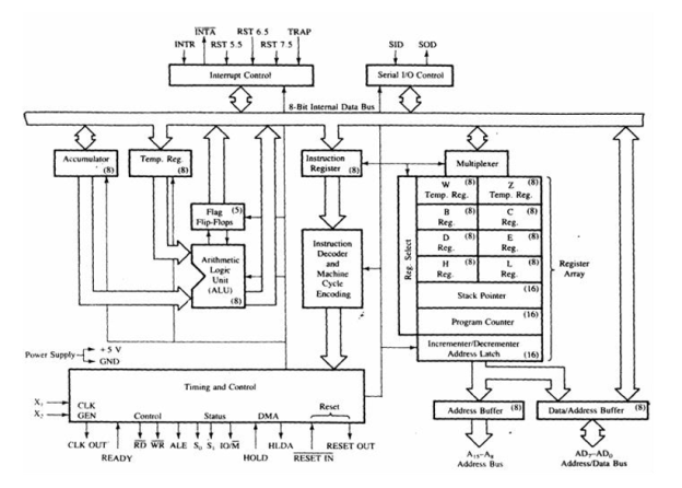
Fig.2: Architecture of 8085
- Address bus A15-A8.
- Data bus AD7-AD0.
- Three control signals are RD, WR & ALE.
- RD: It indicates that the selected IO or memory device can be read and is ready to accept data available on the data bus.
- WR: It indicates that the data on the data bus can be written into a selected memory or IO location.
- ALE: It is a positive going pulse that is generated when a new operation is started by the microprocessor. When high, it indicates address and when low, it indicates data.
- Three status signals are IO/M, S0 & S1.
- IO/
 : It is used for input/output or memory selection i.e. when it is high it indicates IO operation and when it is low then it indicates memory operation.
 - S1 & S0: They are used to identify the type of current operation.
- Power supply: VCC & VSS.
- VCC: +5V and VSS : ground signal (0V).
- Clock signals: There are 3 types of clock signals, X1, X2 and CLK OUT.
- X1, X2: A crystal (RC, LC N/W) is connected at these two pins and is used to set frequency of the internal clock generator. This frequency is internally divided by 2.
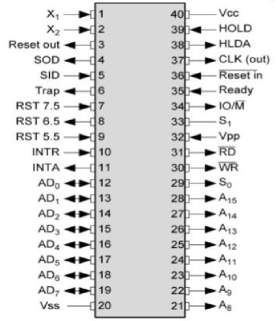
Fig.3: Pin diagram of 8085
- CLK OUT: This signal is used as the system clock for devices connected with the microprocessor.
- Interrupts are the signals generated by external devices requesting the microprocessor to perform a certain task. There are 5 types of interrupt. They are TRAP, RST 7.5, RST 6.5, RST 5.5, and INTR.
- INTA: It is an interrupt acknowledge signal.
- RESET IN: It is used to reset the microprocessor by setting the program counter to zero.
- RESET OUT: It is used to reset all the devices connected to the microprocessor when microprocessor is reset.
- READY: It indicates that the device is ready to send or receive data. If it is low, then the CPU has to wait for it to go high.
- HOLD: It indicates that another master is requesting the use of the address and data buses.
- HLDA: It stands for HOLD Acknowledge. It indicates that the CPU has received the HOLD request and is ready to share the bus in the next clock cycle. After the HOLD signal is removed HLDA is set to low.
- SID and SOD signals are used for serial communication.
- SOD (Serial output data line): It is set/reset by the SIM instruction.
- SID (Serial input data line): when it is active, the data on this line is loaded into accumulator whenever a RIM instruction is executed.
Timing Diagram is a graphical representation. It represents the execution time taken by each instruction in a graphical format. The execution time is represented in T-states.
Instruction Cycle:
The time required to execute an instruction is called instruction cycle.
Machine Cycle:
The time required to access the memory or input/output devices is called machine cycle.
T-State:
The machine cycle and instruction cycle takes multiple clock periods.
A portion of an operation carried out in one system clock period is called as T-state.
An instruction is a binary pattern designed inside a microprocessor to perform a specific function.
- The entire group of instructions that a microprocessor supports is called Instruction Set.
- 8085 has 246instructions.
- Each instruction is represented by an 8-bit binary value.
- These 8-bits of binary value is called Op-Code or Instruction Byte.
It is classified into 5 groups:
- Data Transfer Instruction
These instructions transfer data between registers or between memory and registers. These instructions are used to copy data from source to destination. While copying, the contents of source cannot be modified.
OPCODE | OPERAND | DESCRIPTION |
MOV | Rd, Rs Rd, M M, Rs | Transfer the contents of the source to the destination. |
MVI | Rd, data M, data | Move immediate data into the destination register |
LXI | Reg. Pair, data | Move 16 bit data into the register pair |
LDA | 16 bit address | Load accumulator with data present at the specified address |
XCHG | - | Exchange the contents of HL with DE |
For example: MOV B, C
MVI B, 20H
LXI H, 4020H
LDA 6000H
- Arithmetic Instructions
These instructions perform the operations like:
• Addition
• Subtraction
• Increment
• Decrement
OPCODE | OPERAND | DESCRIPTION |
ADD | R M | Add the contents of register with the contents of accumulator and save in accumulator. |
ADC | R M | Add the contents of register with the contents of accumulator with carry and save in accumulator. |
ADI | 8 bit data | Add data with the content of acc |
DAD | Reg pair | Add register pair to H-L pair |
SUB | R M | Subtract the contents of register with the contents of accumulator and save in accumulator. |
SBB | R M | Subtract the contents of register with borrow from the contents of accumulator and save in accumulator. |
SUI | 8 bit data | Subtract data with the content of acc |
INR | R M | Increment register or memory by 1 |
DCR | R M | Decrement register or memory by 1 |
For example:
ADD C
ADC M
ADI 40H
DAD HL
SUB B
SUI 20H
INR C
- Logical Instructions
The logical operations are:
• AND • OR • XOR • Rotate • Compare • Complement
OPCODE | OPERAND | DESCRIPTION |
CMP | R M | Compare the contents of register or memory with accumulator |
ANA | R M | Logical AND the contents of register with accumulator |
ANI | 8 bit data | Logical AND the data with accumulator |
XRA | R M | XOR the contents of register with accumulator |
ORA | R M | Logical OR the contents of register with accumulator |
RLC | - | Rotate accumulator left |
RRC | - | Rotate accumulator right |
CMA | - | Complement accumulator |
For example:
CMP C
ANA B
ANI 40H
XRA M
ORA C
RLC
- Branching Instructions
These instructions alter the normal sequential flow conditionally or unconditionally.
OPCODE | OPERAND | DESCRIPTION |
JMP | 16 bit address | Jump unconditionally to the given location |
JC | 16 bit address | Jump if carry |
JNC | 16 bit address | Jump if no carry |
JZ | 16 bit address | Jump if zero |
JNZ | 16 bit address | Jump if no zero |
CALL | 16 bit address | Call unconditionally |
RET | - | Return unconditionally |
RST | 0-7 | Restart (Software Interrupts) |
For example:
JMP 2000H
RET
RST 6
- Control Instructions
It controls the operation of microprocessor.
OPCODE | OPERAND | DESCRIPTION |
NOP | - | No operation |
HLT | - | Halt |
DI | - | Disable Interrupt |
EI | - | Enable Interrupt |
RIM | - | Read interrupt mask |
SIM | - | Set interrupt mask |
For example:
NOP
EI
SIM
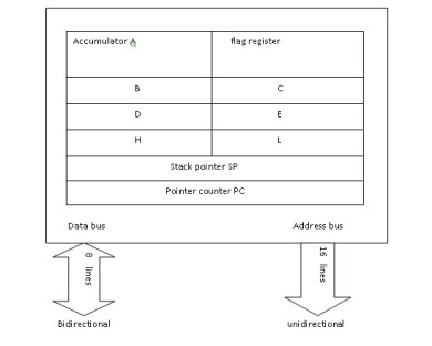
Fig.4: Programmer’s model of 8085
It comprises of:
- Register Array
The general purpose registers are classified into several types such as B, C, D, E, H, & L. They are 8-bit registers. The register pairs are BC, DE & HL.
- Special Purpose Registers
These registers are of four types namely program counter, stack pointer, increment or decrement register, address or data buffer.
Program Counter
It is a 16 bit register. It is used to store data, memory information etc. whenever memory is incremented, the PC then points to the next location.
Stack Pointer
It is a 16 bit register. It always points to stack which can be incremented or decremented by PUSH and POP instruction.
- Flag register
It is an 8 bit register.

Here, Sign (S), Zero (Z), Auxiliary Carry (AC), Parity (P),Carry (C) bit.
- Accumulator
It is an 8-bit register used for performing all arithmetical and logical operations. It is also used to load and store data.
Status Signal (IO/M)
The status signal IO/M resolves whether the address is intended for memory or input/output. When the address is high then the address of the address bus is used for the devices of input/output devices. When the address is low then the address of the address bus is used for the memory.
Status Signals (S0-S1)
The status signals S0, S1 gives different functions as well as status based on their status.
- When the S0, S1 are 01 then the operation will be HALT.
- The S0, S1 is 10 then the operation will be WRITE
- When the S0, S1 is 10 then the operation will be READ
- When the S0, S1 are 11 then the operation will be FETCH
Active Low Signal (RD)
This signal indicates that the selected IO or memory device is to be read and is ready for accepting data available on the data bus.
Active low signal WR
This signal indicates that the data on the data bus is to be written into a selected memory or IO location.
READY
The READY pin is employed for ensuring whether a device is set for accepting or transferring data.
A device may be an A/D converter or LCD display, etc. These devices are associated with the 8085 microprocessors with the READY pin.
When this pin is high, the device is prepared for transferring the information, if it is not then the microprocessor stays until this pin goes high.
HOLD
The signal indicates that another master is requesting the use of address and data buses.
HLDA (Hold Acknowledge)
This signal indicates that CPU has received the HOLD request and it will relinquish the bus in the next clock cycle. HLDA is set to low after HOLD signal is removed.
INTR
This is an interrupt signal, and the priority of this among the interrupt is low. This signal can be allowed or not allowed by the software. When INTR pin goes high then the 8085 microprocessor completes the instruction of current which is being executed and then recognizes the INTR signal and progresses it.
INTA
When the 8085 microprocessor gets an interrupt signal, then it should be recognized. This will be done by INTA. As a result, when the interrupt will be obtained then INTA will go high.
RST 5.5, RST 6.5, RST 7.5
These pins are the restart maskable interrupts or Vectored Interrupts, used to insert an inner restart function repeatedly. All these interrupts are maskable, they can be allowed or not allowed by using programs.
TRAP
Along with the 8085 microprocessor interrupts, TRAP is a non-maskable interrupt, and it doesn’t allow or stopped by a program. TRAP has the maximum precedence between the interrupts. The priority order from maximum to low includes TRAP, RST 5.5, RST 6.5, RST 7.5, and INTR.
RESET IN
RESET IN pin is used to reset the program counter toward zero and rearranges interrupt enable as well as HLDA flip flops (FFs). The central processing unit is detained in RST condition till this pin is high. But the registers as well as flags won’t get damaged apart from instruction register.
RST (RESET) OUT
RESET OUT pin specifies that the central processing unit has been rearranged with RST IN.
X1 X2
X1, X2 terminals that are associated with the exterior oscillator for generating the required as well as appropriate operation of a clock.
CLK
Sometimes it is compulsory to generate CLK o/PS from 8085 microprocessors so they can be used in favour of other peripherals or else other digital integrated circuits. This is offered with CLK pin. Its frequency is continually similar because the frequency at which the microprocessor works.
SID
This is a serial i/p data, and the information on this pin is uploaded into the 7th-bit of the accumulator while RIM (Read Interrupt Mask) instruction is performed. RIM verifies the interrupt whether it is covered or not covered.
SOD
This is the serial o/p data, and the data on this pin sends its output toward the 7th-bit of the accumulator whenever an instruction of SIM is performed.
VSS and VCC
VSS is a ground pin whereas Vcc is +5v pin.
Addressing modes of 8085
The instructions are used to transfer the data from one register to another register, from the memory to the register, and from the register to the memory without any change in the content.
Addressing modes in 8085 is divided into 5 groups −
Immediate addressing mode
Here, the 8/16-bit data is specified in the instruction itself as one of its operand. For example: MVI B, 40F means 40F is copied into register B.
Register addressing mode
Here, the data is copied from one register to another.
For example: MOV B, A: means data in register A is copied to register B.
Direct addressing mode
Here, the data is directly copied from the given address to the register.
For example: LDB 5008H: means the data at address 5008H is copied to register B.
Indirect addressing mode
Here, the data is transferred from one register to another by using the address pointed by the register.
For example: MOV B, K: means data is transferred from the memory address pointed by the register K to the register B.
Implied addressing mode
Here, it doesn’t require any operand; the data is specified by the opcode itself.
For example: CMP.
Memory
Memory is the location where information is kept while not in current use. Memory is a collection of storage devices. Usually, each storage device holds one bit. Also, in most kinds of memory, these storage devices are grouped into groups of 8. These 8 storage locations can only be accessed together. So, one can only read or write in terms of bytes to and from memory.
Memory is usually measured by the number of bytes it can hold. It is measured in Kilos, Megas and lately Gigas. A Kilo in computer language is 210 =1024. So, a KB (Kilobyte) is 1024 bytes. Mega is 1024 Kilos and Giga is 1024 Mega. When a program is entered into a computer, it is stored in memory. Then as the microprocessor starts to execute the instructions, it brings the instructions from memory one at a time.
Memory is also used to hold the data. The microprocessor reads (brings in) the data from memory when it needs it and writes (stores) the results into memory when it is done.
Memory interfacing
Memory is an integral part of a microprocessor system, and in this section, we will discuss how to interface a memory device with the microprocessor. The Memory Interfacing in 8085 is used to access memory quite frequently to read instruction codes and data stored in memory. This read/write operations are monitored by control signals. The microprocessor activates these signals when it wants to read from and write into memory.
The read/write memories consist of an array of registers, in which each register has unique address. The size of the memory is N x M as shown in Fig. (a) where N is the number of registers and M is the word length, in number of bits.
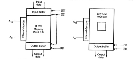
Fig 5. (a) Logic diagram for RAM (b) Logic diagram for EPROM
- Microprocessor 8085 can access 64Kbytes memory since address bus is 16-bit. But it is not always necessary to use full 64Kbytes address space. The total memory size depends upon the application.
- Generally, EPROM (or EPROMs) is used as a program memory and RAM (or RAMs) as a data memory. When both, EPROM and RAM are used, the total address space 64Kbytes is shared by them.
- The capacity of program memory and data memory depends on the application.
- It is not always necessary to select 1 EPROM and 1 RAM. We can have multiple EPROMs and multiple RAMs as per the requirement of application.
- We can place EPROM/RAM anywhere in full 64 Kbytes address space. But program memory (EPROM) should be located from address 0000H since reset address of 8085 microprocessor is 0000H.
- It is not always necessary to locate EPROM and RAM in consecutive memory. For example: If the mapping of EPROM is from 0000H to OFFFH, it is not must to locate RAM from 1000H. We can locate it anywhere between 1000H and FFFFH. Where to locate memory component totally depends on the application.
The memory interfacing requires to:
Select the chip
Identify the register
Enable the appropriate buffer.
Microprocessor system includes memory devices and I/O devices. It is important to note that microprocessor can communicate (read/write) with only one device at a time, since the data, address and control buses are common for all the devices. In order to communicate with memory or I/O devices, it is necessary to decode the address from the microprocessor. Due to this each device (memory or I/O) can be accessed independently.
Memory mapped I/O
In memory mapped I/O, the I/O devices are assigned and identified by 16-bit addresses. The memory related instructions transfer the data between an I/O device and the microprocessor, as long as I/O port is assigned to the memory address space rather than to the I/O address space. The register associated with the I/O port is simply treated as a memory location. Thus I/O device becomes a part of the system’s memory map and hence its name.
In memory-mapped I/O every instruction that refers to a memory location can control I/O. The source and destination of the data is limited with I/O mapped I/O, since for an IN instruction the destination register is always the accumulator, and for the OUT instruction the source register is always the accumulator. However, for memory mapped I/O there are number of sources and destinations.
Interfacing of I/O port with memory mapped I/O:
In memory mapped I/O, MEMR (memory read) and MEMW (memory write) control signals are required to control the data transfer between I/O device and microprocessor. As 8085 gives 16-bit memory address, it is necessary to decode 16-bit memory address to generate device select signal in case of memory mapped I/O. Fig. Shows the Input Output Interfacing Techniques devices in memory mapped I/O mode.
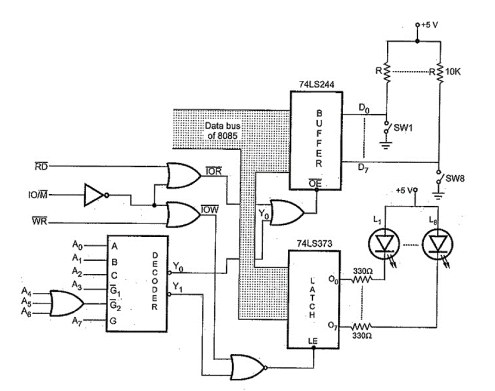
Figure 6: I/O interfacing using I/O Mapped I/O
Input & output devices
The Input Output devices gets connected to a computer through the Input Output ports. Two Instructions are fetched which are called as IN and OUT where there are 256 Input Ports and 256 Output ports. For the communication with a printer, the CPU loads the output port connected to the printer which works at electronic speeds. The printer prints the total information at about 15-20 s.
I/O port chip with a single port is shown below.
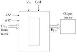
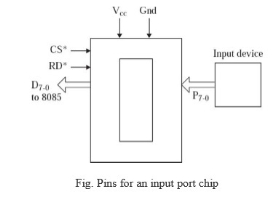
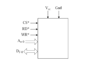
Fig.7: I/O port chip
In 8085 Instruction set, there are two instructions in 8085 for communication with I/O ports. They are the IN and OUT instructions. The IN or OUT instruction mnemonic should be followed by an 8-bit port address. Thus, we can have 2 8 = 256 input ports and 256 output ports are possible in 8085-based microcomputer. IN and OUT both are 2-Byte’s instructions.
Mnemonics, Operand | Opcode (in HEX) | Bytes |
IN Port-address | DB | 2 |
OUT Port-Address | D3 | 2 |
In case of IN instruction, the current 8-bit content of the PORT# will be made available on to the Accumulator.
Let us suppose with the PORT#, 8 DIP switches are connected. And their states are ON-ON-OFF-ON-ON-ON-OFF-ON. So, after execution of the instruction IN PORT#, the Accumulator content will be 1101 1101.
In case of OUT instruction, the current 8-bit content of the Accumulator will be copied on to the PORT#. Let us suppose that Accumulator’s initial content is 0101 0101. And with the 8-bit port 8 LEDs are connected. So, after execution of the instruction OUT PORT#, LEDs will have the states as shown.

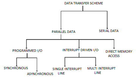
Fig.8: Data transfer schemes
Interruption can be done at the time of executing program by the virtue of the program by an Input Output device.
It can also be done by the method as per the working of the processor.
The data transfer schemes wants sending information to the processor, rather than receiving information from the processor because sending and receiving information plays a vital role for executing the entire program.
The communication is not done directly with the Input Output device. It is carried out systematically with the help of Input Output device by the virtue of an Input Output port. The data transfer schemes are as follows:
Serial data transfer scheme
In serial I/O mode transfer, a single bit of data is present on a single line at a time.
In serial transmission of data, 8-bit parallel word is converted to a stream of eight serial bit using parallel-to-serial converter.
Similarly, in serial reception of data, a stream of 8-bit is received one by one which are then converted to 8- bit parallel word using serial-to-parallel converter.
Parallel data transfer scheme
It is faster than serial I/O transfer.
In this, 8-bit data is send across 8 parallel wires.
Programmed I/O Data Transfer
- It is a simple parallel data transfer scheme.
- It is generally used in the simple microprocessor systems where speed is unimportant.
- It uses instructions to get the data in or out of the microprocessor.
- It works on synchronous or asynchronous mode depending upon the type and the speed of the I/O devices.
Synchronous type of data transfer
- It is used when the speed of the I/O devices matches with the speed of the 8085 microprocessor.
- A common clock pulse is required for synchronization.
- This clock pulse synchronizes the microprocessor and the I/O devices.
- It is called as Synchronous type of data transfer scheme because of the matching of the speed as the microprocessor does not have to wait for the data.
- The microprocessor immediately sends data as soon as the signal is issued.
Asynchronous type data transfer
- It is used when the speed of the I/O devices is slower than the speed of the microprocessor.
- Hence, the internal timing of the I/O device is independent from the microprocessor.
- It is normally implemented using ‘handshaking’ mode.
- In the handshaking mode, some signals are exchanged before the data transfer takes place between the I/O device and microprocessor.
Interrupt Driven I/O Data Transfer
It is a very efficient method as no microprocessor time is wasted in waiting for an I/O device to be ready.
In this, the I/O device informs the microprocessor for the data transfer whenever the I/O device is ready. This is achieved by interrupting the microprocessor.
Whenever the device is ready to accept or supply data, it informs the processor through an (INTR) control signal.
In response to this, the microprocessor sends back an interrupt acknowledge (INT A) signal to the I/O device.
It suspends its job after executing the current instruction and saves the contents and status of program counter.
Several input/output devices may be connected to microprocessor using the above scheme. Following interrupt request configuration are there while interfacing the I/O devices to microprocessor.
- Single Interrupt system
- Multi Interrupt System
Single Interrupt System
In this, only one interrupt line is available and several I/O devices are to be connected.
Multi Interrupt System
Here, the microprocessor has several interrupt terminals and one I/O device is to be connected to each interrupt terminal, then it is known as multi interrupt system.
Direct Memory Access (DMA) Data Transfer
DMA is used for bulk data transfer from I/O devices to microprocessor or vice-versa.
In this method I/O devices are allowed to transfer the data directly to the external memory without being routed through accumulator.
The microprocessor relinquishes the control over the data bus and address bus, so that these can be used for transfer of data between the devices.
Working principle of direct memory access data transfer
For this data transfer, a request to the microprocessor in form of HOLD signal, by the I/O device is sent.
When microprocessor receives such request, it relinquishes the address and data buses and informs the I/O devices of the situation by sending Acknowledge signal HLDA.
The I/O device then withdraws the request when the data transfer between the I/O device and external memory is complete.
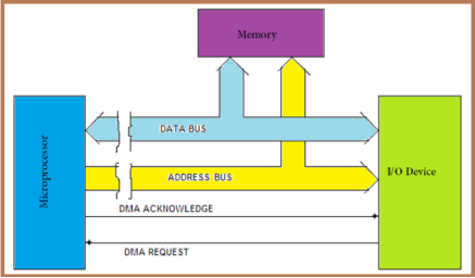
Fig.9: DMA
8255 Chip
Pin Configuration
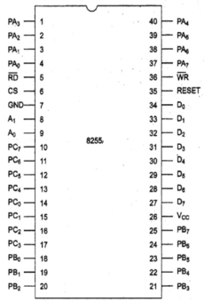
Fig.10 : Pin Configuration of 8255
- It is also known as Programmable Peripheral Interface.
- It is a multi port device.
- It has 24 I/O pins. They are divided into three 8 bit ports PA, PB, PC.
- Port A and port B are used as 8-bit I/O ports.
- Port C is used as an 8-bit I/O port or as two 4-bit I/O ports or produces handshake signals for ports A and B.
- CS: The chip select CS (pin 6) is used to enable the 8255 chip. It is an active-low signal, hence is enabled when CS = 0.
- RESET: It is an input pin 35 and is connected to the RESET line of system 8085. When the system is reset, all the ports behave as input lines. This is done to prevent 8255 from being destroyed due to mismatch of ports.
- Eight data lines (D0–D7) are available to read/write data into the ports or control register under the status of the RD (pin 5) and WR (pin 36), which are active-low signals for read and write operations respectively.
- Address lines A1 and A0 allow to access a data register for each port or a control register, as listed below:
A1 | A0 | PORT SELECTED |
0 | 0 | PORT A |
0 | 1 | PORT B |
1 | 0 | PORT C |
1 | 1 | Control Register |
Operating Modes
There are two basic operating modes of 8255.
- Bit set/reset mode (BSR mode)
- Input/ output mode (I/O mode)
The modes selected by the D7 bit of the control word register are:
When D7 = 1, 8255 operates in I/O mode else BSR mode.
BSR MODE
The Bit Set/Reset (BSR) mode is available on port C only. Each and every line of port C (PC7 - PC0) can be set or reset by providing a suitable value to the control word register. BSR mode is independent and its selection does not affect the operation of other ports in I/O mode.

- D7 bit is always 0 for this mode.
- Bits D6, D5 and D4 are don't care bits.
- Bits D3, D2 and D1 are used for pin selection of Port C.
- Bit D0 is used to set/reset the above selected pin.
Selection of port C pin is determined as follows:
D3 | D2 | D1 | Bit/pin of port C selected |
0 | 0 | 0 | PC0 |
0 | 0 | 1 | PC1 |
0 | 1 | 0 | PC2 |
0 | 1 | 1 | PC3 |
1 | 0 | 0 | PC4 |
1 | 0 | 1 | PC5 |
1 | 1 | 0 | PC6 |
1 | 1 | 1 | PC7 |
For example:
If PC4 be set, then in the control word is,
- Since it is a BSR mode, D7 = '0'.
- Since D4, D5, D6 are don’t care hence assuming them to be '0'.
- PC4 has to be selected, hence, D3 = '1', D2 = '0', D1 = '0'.
- PC4 has to be set, hence, D0 = '1'.
Thus, as per the above values, 0AH (in hex) will be loaded into the Control Word Register (CWR).
I/O MODE
When D7 bit of the Control Word Register is 1, this mode is selected.
There are three I/O modes and they are:
- Mode 0 - Simple I/O
- Mode 1 - Strobed I/O
- Mode 2 - Strobed Bi-directional I/O
- Mode 0 – Simple or basic I/O mode:
Port A, B and C can work either as input or as output function. The outputs are latched but the inputs are not latched. It can handle interrupts.
- Mode 1 – Handshake or strobbed I/O:
Here, either port A or B can work and port C is used to provide handshake signals. The outputs as well as inputs are latched. It can handle interrupts. Before actual data is transmitted, there is transmission of signal to match speed of CPU and printer.
- Mode 2 – Bidirectional I/O:
In this mode only port A will work, port B can either is in mode 0 or 1 and port C bits are used as handshake signal. The outputs as well as inputs are latched. It has interrupt handling capability.
Control Word for I/O mode
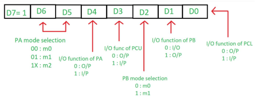
The most significant bit (D7) is 1 for the I/O mode.
D6 & D5: It is used to set the port A mode.
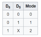
- D4: It is used to check whether port A is taking input or displaying the output. If it is 1 then input else output.
- D3: It is used to check whether port C higher bites takes input or output. If 1, then input else output.
- D2: It tells the mode of port B. If 0, then port B is in M0 mode else in M1 mode.
- D1: It is used to check whether port B is taking input or displaying output. If 1, then input else output.
- D0: It is used to tell whether port C lower bits is taking input or displaying output. If 1, then it takes input else displays output.
When 8255 microprocessor is reset, it clears the control word register contents and sets all the ports to input mode.
8251 Chip
It is commonly known as USART (Universal Synchronous Asynchronous Receiver Transmitter).
Pin Configuration
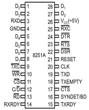
Fig. 11: Pin diagram of 8251
- D0 – D7: Bi-directional 8 bit data lines.
- RD and WR: They are active low signal. When RD is low, CPU can read the data and when WR is low then CPU can write the data.
- CLK: A clock is used to generate internal device timing. Its frequency must be 3 times the data transmission or reception rate.
- RESET: A high on this, forces 8251 into idle mode.
- C/D: It is Control/ Data. It with combination of RD and WR, informs 8251 about the word on the data bus is either data character control word or status information given below:
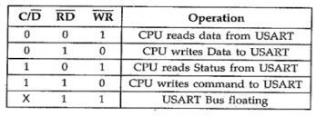
- CS (Chip Select): It is an active low pin and is responsible for the communication between CPU and 8251.
- DSR (Data Set Ready): It is used to test the modem conditions.
- DTR (Data Terminal Ready): This output signal tells the modem that data terminal is ready for transmission.
- RTS (Request To Send): It is used to start the transmission.
- CTS (Clear To Send): It is used to transmit serial data when 0.
- TxD (Transmit Data): It transmits a composite serial stream of data on the falling edge of the TxC.
- TxRDY (Transmitter Ready): If 1, the transmitter is ready to accept data character.
- TxE (Transmitter Empty): It indicates that the transmitter has no character to transmit.
- TxC (Transmitter Clock): It is used to control the transmission rate of the character.
- RxD (Receiver Data): It receives a composite serial stream of data on the falling rising edge of the RxC.
- RxRDY (Receiver Ready): It indicates that the character is ready to be input to the CPU.
- RxC (Receiver Clock): It is used to control the reception rate of the character.
- SYNDET/ BRKDET: It is used as synchronous detect or break detect.
Control Word
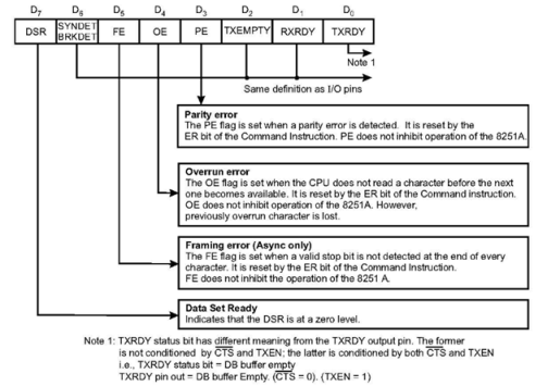
Fig. 12: Bit configuration of control word
Operating Modes
There are two modes of operation:
- Mode instruction (setting of function)
- Command (setting of operation)
Mode instruction (setting of function)
It is used to set the function of the 8251. It will be in "wait for write" at either internal reset or external reset which means that writing a control word after reset will be recognized as a "mode instruction."
Items that can be set by mode instruction are:
• Synchronous/asynchronous mode
• Stop bit length (asynchronous mode)
• Character length
• Parity bit
• Baud rate factor (asynchronous mode)
• Internal/external synchronization (synchronous mode)
• Number of synchronous characters (Synchronous mode)
In the case of synchronous mode, it is necessary to write one-or two byte sync characters. If sync characters were written, a function will be set because the writing of sync characters constitutes part of mode instruction.
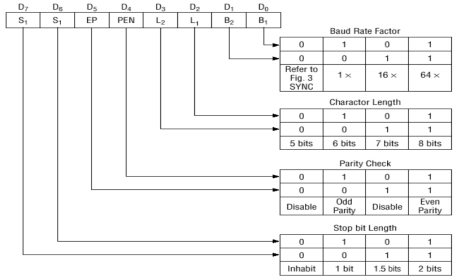
Fig. 13: Bit configuration of Mode instruction (Asynchronous)
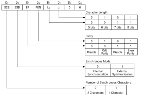
Fig. 14: Bit configuration of Mode instruction (synchronous)
Command (setting of operation)
It is used to set the operation of the 8251. Items that are set by command are as follows:
• Transmit Enable/Disable
• Receive Enable/Disable
• DTR, RTS Output of data.
• Resetting of error flag.
• Sending to break characters
• Internal resetting
• Hunt mode (synchronous mode)
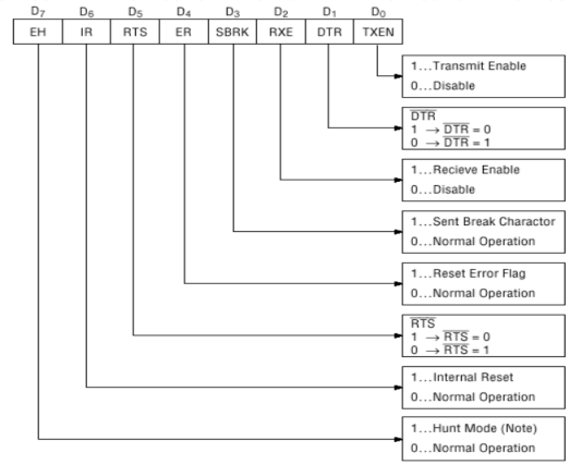
Fig. 15: Bit configuration of Command
8253 Chip
Pin Configuration

Fig.16: Pin Configuration of 8253
It is a programmable counter / timer chip which is used as an Intel microcomputer peripheral.
It uses nMOS technology with +5V supply and is packaged in a 24-pin plastic DIP. It is used as an event counter, elapsed time indicator, programmable one-shot etc.
There are three counters, a data bus buffer, Read/Write control logic, and a control register. Each counter has two input signals - CLOCK & GATE, and one output signal - OUT.
Data Bus Buffer
It is a tri-state, bi-directional, 8-bit buffer, which is used to interface the 8253 to the system data bus. It has three basic functions −
- Programming the modes of 8253.
- Loading the count registers.
- Reading the count values.
Read/Write Logic
It includes 5 signals, i.e. RD, WR, CS, and the address lines A0 & A1. In the peripheral I/O mode, the RD and WR signals are connected to IOR and IOW and in the memory mapped I/O mode to MEMR and MEMW.
Address lines A0 & A1 of the CPU are connected to lines A0 and A1 of the 8253 and CS is tied to a decoded address.
A1 | A0 | Result |
0 | 0 | Counter 0 |
0 | 1 | Counter 1 |
1 | 0 | Counter 2 |
1 | 1 | Control Word Register |
X | X | No Selection |
Control Word Register
This register can be accessed when lines A0 & A1 are at logic 1.
It is used to write a command word, its mode and either a read or write operation.
Following table provides the result for various control inputs:
A1 | A0 | RD | WR | CS | Result |
0 | 0 | 1 | 0 | 0 | Write Counter 0 |
0 | 1 | 1 | 0 | 0 | Write Counter 1 |
1 | 0 | 1 | 0 | 0 | Write Counter 2 |
1 | 1 | 1 | 0 | 0 | Write Control Word |
0 | 0 | 0 | 1 | 0 | Read Counter 0 |
0 | 1 | 0 | 1 | 0 | Read Counter 1 |
1 | 0 | 0 | 1 | 0 | Read Counter 2 |
1 | 1 | 0 | 1 | 0 | No operation |
X | X | 1 | 1 | 0 | No operation |
X | X | X | X | 1 | No operation |
Operating Modes
8253 can be operated in 6 different modes. They are:
Mode 0 ─ Interrupt on Terminal Count
- It is used for generating an interrupt to the microprocessor after a certain interval.
- The output is low after the mode is set and remains LOW after the count value is loaded into the counter.
- The counter decrement continues till the terminal count is reached.
- The GATE signal remains high for normal counting. When it is low, counting is terminated and the current count is latched till it goes high again.
Mode 1 – Programmable One Shot
- It is used as a mono stable multi-vibrator.
- GATE is used as a trigger input in this mode.
- As the count is loaded the output remains high and a trigger is applied.
Mode 2 – Rate Generator
- The output is high after initialization.
- Whenever the count becomes zero, a low pulse is generated at the output and the counter is reloaded.
Mode 3 – Square Wave Generator
- This mode is same as Mode 2 except that the output remains low for half of the timer period and high for the next half of the period.
Mode 4 − Software Triggered Mode
- In this, the output remains high till the timer counts to zero and at this point the output is low and then goes high again.
- The count is latched when GATE LOW.
- As per the terminal count, for one clock cycle the output goes low then goes HIGH. The low pulse is used as a strobe.
Mode 5 – Hardware Triggered Mode
- This mode generates a strobe as a result to an externally generated signal.
- It is same as mode 4 except that the counting is initiated by a signal at the gate input.
- As soon as it is initialized, the output goes high.
- When the terminal count is reached, the output goes low for one clock cycle.
I/O port
Any application of 8085 requires the transfer of data between external circuitry to the microprocessor and vice versa. User can provide information to the microprocessor with the help of keyboard and can see the result on a display device.
Hence, the transfer of data between the input, microprocessor and output is known as Input Output Interfacing or I/O data transfer.
INPUT PORT
- It is used to read data from the input device like mouse, keyboard etc.
- The simplest input port is a buffer.
- A buffer is used to connect input device with the microprocessor.
- It is a tri-state buffer and its output is available when ENABLE is active.
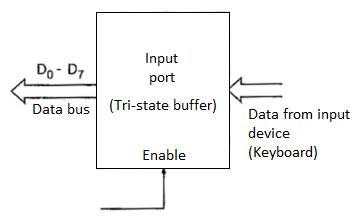
Fig.17: Input port
- The control signals from the microprocessor activate the buffer when microprocessor wants to read the input device.
- As soon as the buffer is enabled, data is available on the data bus.
- The data is then read by the microprocessor using READ command.
OUTPUT PORT
- It is used to send data to the output device like display.
- The simplest output port is a latch.
- Figure below shows the output device connected to the microprocessor with the latch.
- When microprocessor wants to send data, it puts the data on the data bus and activates the clock signal of the latch.
- It is available at the output of the latch for the output device.
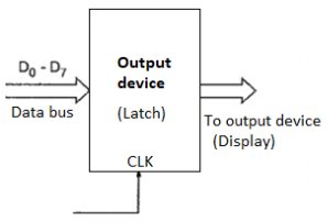
Fig.18: Output port
References:
- Microprocessor Architecture, Programming, and ...Book by Ramesh S. Gaonkar
- 8085 Microprocessor: Programming and Interfacing Book by N. K. Srinath
- 8085 Microprocessors & Its Application Book by Nagoorkani