Unit - 3
The 8051 Architecture
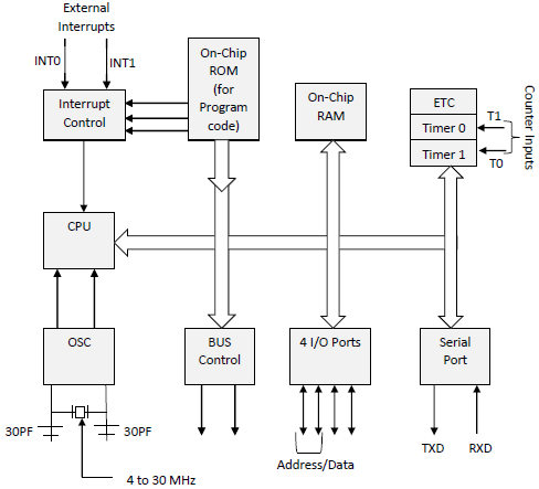
In the following diagram, the system bus connects all the support devices to the CPU. The system bus consists of an 8-bit data bus, a 16-bit address bus and bus control signals. All other devices like program memory, ports, data memory, serial interface, interrupt control, timers, and the CPU are all interfaced together through the system bus.
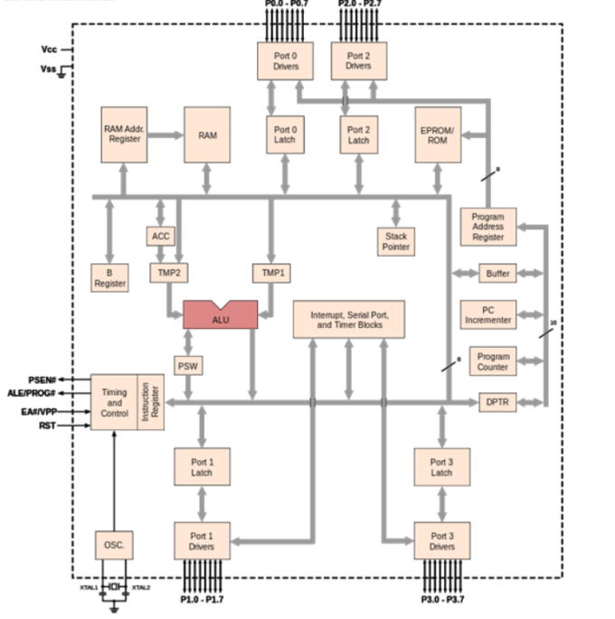
8051 microcontrollers were designed by Intel in 1981. It is an 8-bit microcontroller. It is built with 40 pins DIP (dual inline package), 4kb of ROM storage and 128 bytes of RAM storage, 2 16-bit timers. It consists of four parallel 8-bit ports, which are programmable as well as addressable as per the requirement.
The reasons for the popularity of 8051 Microcontroller are –
● Simple to integrate in any electronic device.
● Affordable.
● Simple architecture.
● Easy instruction set.
● Low computing power.
The CPU acts as a mind of any processing machine. It synchronizes and manages all processes that are carried out in microcontrollers. The user has no power to control the functioning of the CPU. It interprets the program stored in ROM and carries out from storage and then performs it projected duty. CPUs manage the different types of registers available in 8051 microcontrollers.
It is the heart of the Microcontroller that mainly comprises an Arithmetic Logic Unit (ALU) and a Control Unit (CU) and other important components. The CPU is the primary device in communicating with peripheral devices like Memory, Input and Output.
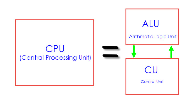
ALU performs all arithmetic and logical functions.
Addition, subtraction with carry, and multiplication are categorized as arithmetic operations.
Logical AND, OR and exclusive OR (XOR) as logical operations.
A bus consists of a group of wires to transfer data from one location to another within the system. Buses reduce the number of paths or cables needed to set up connection between components.
There are two kinds of buses - Data Bus and Address Bus
Data Bus: The purpose of a data bus is to transfer data. It acts as a channel for data to travel.
Address Bus: The purpose of address bus is to transfer information but not data. The information tells from where within the components, the data should be sent to or received from.
Control bus - carries control signals from the processor to other components. The control bus also carries the clock's pulses. The control bus is unidirectional
The pin diagram of 8051 microcontroller looks as follows −
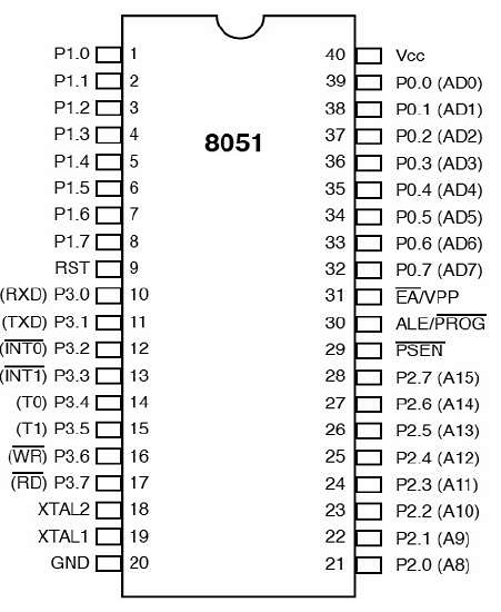
- Pins 1 to 8 − These pins are known as Port 1. This port doesn’t serve any other functions. It is internally pulled up, bi-directional I/O port.
- Pin 9 − It is a RESET pin, which is used to reset the microcontroller to its initial values.
- Pins 10 to 17 − These pins are known as Port 3. This port serves some functions like interrupts, timer input, control signals, serial communication signals RxD and TxD, etc.
- Pins 18 & 19 − These pins are used for interfacing an external crystal to get the system clock.
- Pin 20 − This pin provides the power supply to the circuit.
- Pins 21 to 28 − These pins are known as Port 2. It serves as I/O port. Higher order address bus signals are also multiplexed using this port.
- Pin 29 − This is PSEN pin which stands for Program Store Enable. It is used to read a signal from the external program memory.
- Pin 30 − This is EA pin which stands for External Access input. It is used to enable/disable the external memory interfacing.
- Pin 31 − This is ALE pin which stands for Address Latch Enable. It is used to demultiplex the address-data signal of port.
- Pins 32 to 39 − These pins are known as Port 0. It serves as I/O port. Lower order address and data bus signals are multiplexed using this port.
- Pin 40 − This pin is used to provide power supply to the circuit.
8051 microcontrollers have 4 I/O ports each of 8-bits configured as input or output. Hence, total 32 input/output pins allow the microcontroller to be connected with the peripheral devices.
● Pin configuration, that is the pin is configured as 1 for input and 0 for output as per the logic state.
- Input/Output (I/O) pin − All the circuits within the microcontroller must be connected to one of its pins except P0 port because it does not have pull-up resistors built-in.
- Input pin − Logic 1 is applied to a bit of the P register. The output FE transistor is turned off and the other pin remains connected to the power supply voltage over a pull-up resistor of high resistance.
● Port 0 − The P0 (zero) port is characterized by two functions −
- When the external memory is used then the lower address byte (addresses A0A7) is applied on it, else all bits of this port are configured as input/output.
- When P0 port is configured as an output then other ports consisting of pins with built-in pull-up resistor connected by its end to 5V power supply, the pins of this port have this resistor left out.
Input Configuration
If any pin of this port is configured as an input, then it acts as “floats” , that is the input has unlimited input resistance and in-determined potential.
Output Configuration
When the pin is configured as an output, then it acts as an “open drain”. By applying logic 0 to a port bit then appropriate pin will be connected to ground (0V), and applying logic 1, the external output will keep on “floating”.
To apply logic 1 (5V) on this output pin, it is necessary to build an external pullup resistor.
Port 1
P1 is a true I/O port as it does not have any alternative functions as in P0, but this port can be configured as general I/O only. It has a built-in pull-up resistor and is completely compatible with TTL circuits.
Port 2
P2 similar to P0 when the external memory is used. Pins of this port occupy addresses intended for the external memory chip. This port can be used for higher address byte with addresses A8-A15. When no memory is added then this port can be used as a general input/output port similar to Port 1.
Port 3
In this port, functions are similar to other ports except that the logic 1 must be applied to the appropriate bit of the P3 register.
8051 has five interrupts. These are INT0, INT1, T0, T1, TI/RI. All these interrupts can be enabled or disabled by IE (interrupt enable) register.
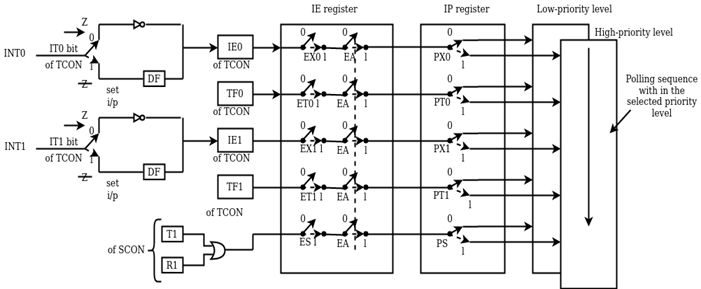
Figure. Interrupt Structure of 8051.
Interrupt Enable (IE)Register
This register can be used to enable or disable interrupts by programming. It is an SFR with address A8H. This byte is bit addressable hence can be programmed by the user. Every bit in this register has a specific meaning.


Interrupt Priority (IP) Register
The five interrupts can be either one or two interrupt level. The priority levels are level 1 and level 0. Higher Priority is indicated by level 1 and level 0 indicates lower priority. To store priority levels for each interrupt IP register is used. This is bit addressable SFR with address B8H.


External Interrupt
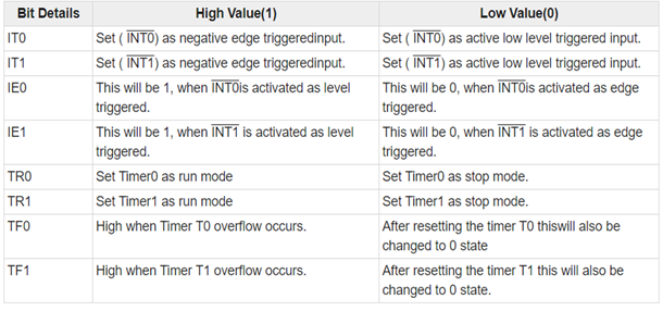
The external interrupts are INT0 and INT1. The TCON register can be used to program external interrupts to edge or level triggered. The TCON is Timer Control. TCON is another bit addressable SFR. The address is 88H.
Key takeaway
Interrupt is a subroutine call that interrupts the microcontroller's main operations or work and causes it to execute any other program, at the time of operation. It provides a mechanism to put on hold the ongoing operations, execute a subroutine and resume to another type of operation.
8051 has five interrupts as mentioned below:
- INTO
- TFO
- INT1
- TF1
- R1/T1
The interrupts (INT0) ̅ and (INT1) ̅ are called as external interrupts. The interrupts (INT0) ̅ and (INT1) ̅ are negative edge triggered. When, these interrupts are activated, the corresponding flags are set except for serial interrupts.
8051 has four ports P0,P1,P2,P3. They are required for I/O operations.
32 pins are set for four ports P0,P1,P2,P3. Each port takes 8 pins.
All the ports are configured as input upon Reset
When zero is written to port it becomes output. To make it input 1 needs to be sent to the port.
Port 0:
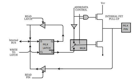
Fig. Port -0
When Port0 is used as input port 1 must be written to the corresponding zero latch that causes the output transistor to switch off and pin floats in high impedance state.
When configured as input port it provides two facilities:
Reads logic level on physical pin by asserting read pin signal.
Read contents of internal latch by asserting the read latch signal.
The latch is read for instruction read-modify-write type instruction.
It reads data from the port modifies and writes to the port.
When Port0 is configured as output the latch pins that are programmed to 0 will cause the lower FET to turn ON and pin is grounded.
If 1 is written to the latch pin FET will turn OFF and pin is pulled HIGH by external pull-up resistor.
Port 1:
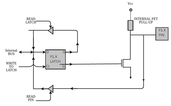
Figure. Port 1 circuit
When port 1 is used as in input port ‘1’ must be written to the corresponding port1 latch bit. This causes the lower FET to turn off.
The pin and the input buffer are pulled to logic HIGH by internal pull load.
This port is called quasi-bidirectional port because its output is pulled high with pull up resistor.
When port 1 is used as an output port, the latch pins that are programmed to 0, will cause the lower FET turn on the internal pull to turn off and input is logic 0.
If 1 is written onto the latch, then it will drive the input of external circuit high through pull up. The lower FET turns off.
Port 2:
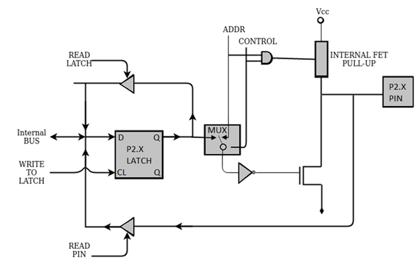
Figure. Port 2 circuit
When Port2 is used as an input port 1 must be written to the corresponding latch bit. This causes the FET turn off. The pin and input to pin buffer are pulled to logic high by internal pull up load.
Port 2 is called as “quasi-bidirectional port” as its output is pull up resistors.
When port2 is used as output port the latch pins that are programmed to 0, will cause the lower FET to turn off and input to the circuit logic 0.
If “1” is written onto latch pin, then it will drive the input of external circuit high through pull-up. The lower FET turns off.
Port 3:
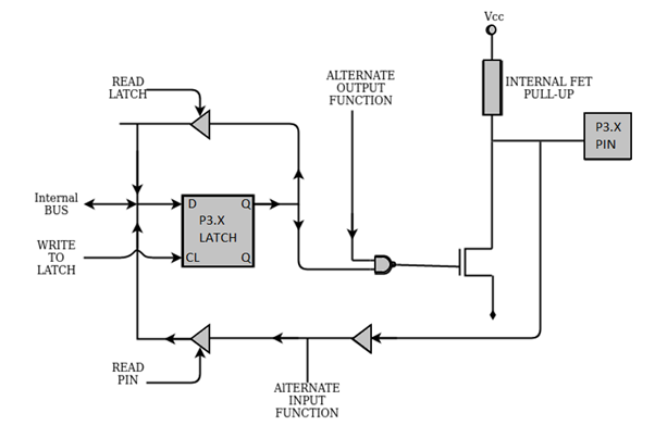
Figure. Port 3 circuit
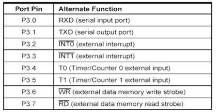
When port3 is used as input port 1 must be written to the corresponding port3 latch bit.
This causes FET to turn off.
The pin and input to the buffer are pulled to logic HIGH by internal pull up load.
When port3 is used as output port, the latched pins that are programmed to 0 will cause to lower FET to turn on and internal pull up to turn off and input to circuit is logic 0.
If 1 is written onto latch pin it will drive the input external circuit high through pull up. The lower FET turns off.
Key takeaway
- A special area of data in memory. The stack pointer is an 8-bit register whose main function is to access the stack. It can take values in the range 00 H to FF H. SP acts as a pointer to points to an address at the top of the stack.
- When Port0 is used as input port 1 must be written to the corresponding zero latch that causes the output transistor to switch off and pin floats in high impedance state.
The 8051 Microcontroller Memory is separated into Program Memory (ROM) and Data Memory (RAM). The Program Memory of the 8051 Microcontroller is used for storing the program to be executed, which means instructions. The Data Memory is used for storing temporary variable data and intermediate results.
Program Memory (ROM) of 8051
The code or instructions which are to be executed are stored in the Program Memory, also called as the ROM of the Microcontroller.
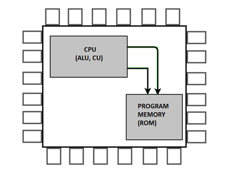
Figure. Program Memory
In 4KB Internal ROM, the address space is 0000H to 0FFFH. If the program addresses exceed this value, CPU will automatically fetch the code from the external Program Memory.
For External Access (EA Pin) must be pulled HIGH at this condition the CPU first fetches instructions from the Internal Program Memory in the address range of 0000H to 0FFFFH. If it exceeds the memory addresses limit, instructions are fetched from external ROM in address range of 1000H to FFFFH.
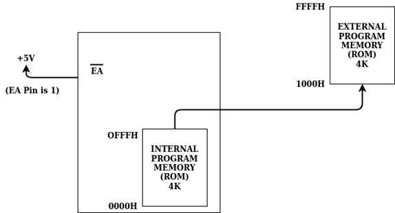
Figure. External access
There is also an alternative method to fetch the instructions where the Internal ROM is ignored and instructions are fetched only from External Program Memory (External ROM).
For this purpose, EA pin must be connected to GND. The memory addresses of external ROM will be from 0000H to FFFFH.
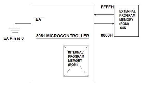
Figure. External Program Memory
Data Memory (RAM)
Data Memory or RAM stores temporary data and intermediate results generated during the normal operation of the microcontroller.
Currently, 8051 Microcontroller has 256B of RAM. The first 128B memory addresses from 00H to 7FH is divided in to Working Registers. They are organized as Register Banks, Bit – Addressable Area and General-Purpose RAM known as Scratchpad area.
The first 128B of RAM (from 00H to 7FH), the first 32B of memory from addresses 00H to 1FH consists of 32 Working Registers organized into four banks with 8 Registers in each Bank.
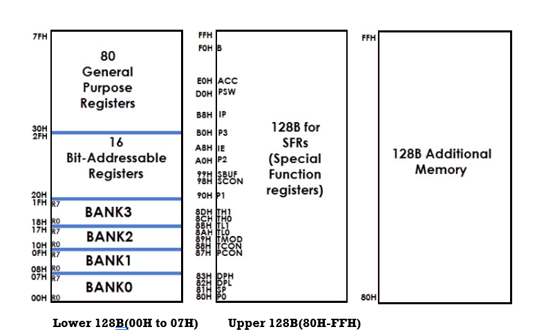
Fig. (Direct and Indirect Addressing) (Direct Addressing) (Indirect Addressing)
The 4 banks are named as Bank0, Bank1, Bank2 and Bank3. Each Bank consists of 8 registers R0 – R7. Each Register can be addressed either by name or by address.
To address the register by name, first the corresponding bank is selected. In order to select the bank, RS0 and RS1 bits of the Program Status Word (PSW) and Register (RS0 and RS1 are 3rd and 4th bits in the PSW Register) are used.
When addressing these Register for example 12H the corresponding bank may or may not be selected. (12H corresponds to R2 in Bank2).
The next 16B of the RAM that is from 20H to 2FH are Bit – Addressable memory locations. A total of 128 bits can be addressed individually using 00H to 7FH or an entire byte can be addressed as 20H to 2FH.
The final 80B of the internal RAM addresses are from 30H to 7FH which is the general-purpose RAM area are byte addressable.
These lower 128B of RAM can be addressed directly or indirectly.
Key takeaway
- For External Access (EA Pin) must be pulled HIGH at this condition the CPU first fetches instructions from the Internal Program Memory in the address range of 0000H to 0FFFFH. If it exceeds the memory addresses limit, instructions are fetched from external ROM in address range of 1000H to FFFFH.
- Currently, 8051 Microcontroller has 256B of RAM. The first 128B memory addresses from 00H to 7FH is divided in to Working Registers.
The processor decodes the instruction in the instruction register and generates the necessary control signals to execute the instruction. Based on the instruction further operations such as fetching, writing into memory etc takes place.
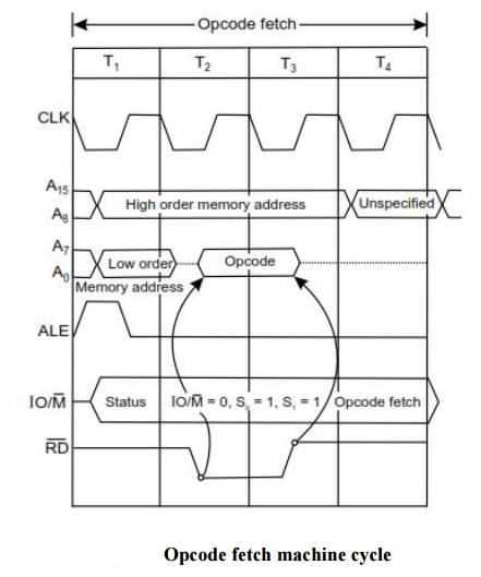
Fig. Timing diagram for op-code fetch cycle
Memory Read Machine Cycle:
The memory read cycle is executed by the processor to read a data byte from memory.
The machine cycle is exactly same to opcode fetch except:
a) It has three T-states
b) The S0 signal is set to 0.
The timing diagram of this cycle is given in
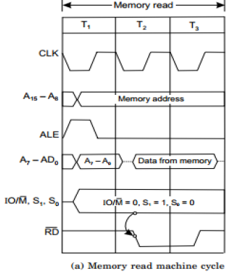
Fig. Timing diagram for memory read machine cycle
Memory Write Machine Cycle:
The memory write cycle is executed by the processor to write a data byte in a memory location. The processor takes three T-states and ^(WR) signal is made low. The timing diagram of this cycle is given in Figure.

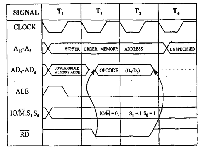
I/O Read Cycle:
The I/O read cycle is executed by the processor to read a data byte from I/O port or from peripheral, which is I/O mapped in the system. The 8-bit port address is placed both in the lower and higher order address bus. The processor takes three T-states to execute this machine cycle. The timing diagram of this cycle is given in Figure
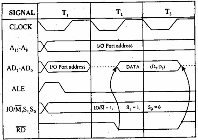
Fig. I/O read machine cycle
Program Memory (ROM) of 8051
The code or instructions which are to be executed are stored in the Program Memory, also called as the ROM of the Microcontroller.
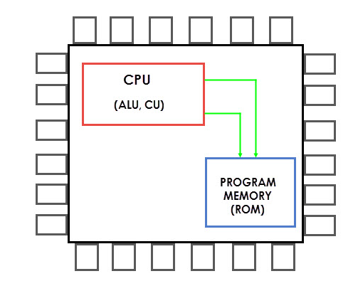
Fig. Program Memory
In 4KB Internal ROM, the address space is 0000H to 0FFFH. If the program addresses exceed this value, the CPU will automatically fetch the code from the external Program Memory.
For External Access (EA Pin) must be pulled HIGH at this condition the CPU first fetches instructions from the Internal Program Memory in the address range of 0000H to 0FFFFH .If it exceeds the memory addresses limit, instructions are fetched from external ROM in address range of 1000H to FFFFH.
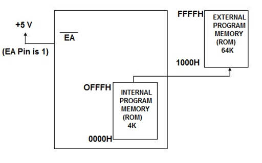
Fig. External access
There is also an alternative method to fetch the instructions where the Internal ROM is ignored and instructions are fetched only from External Program Memory(External ROM).
For this purpose, the EA pin must be connected to GND. The memory addresses of external ROM will be from 0000H to FFFFH.
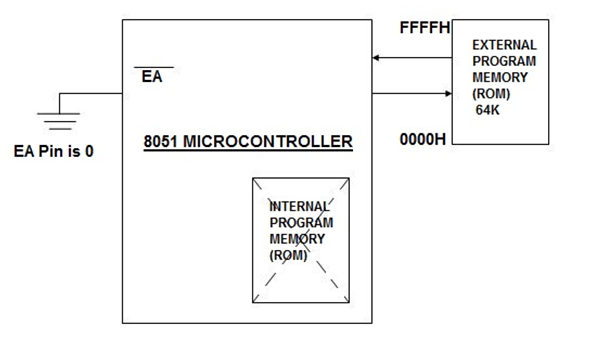
Fig. External Program Memory
Data Memory (RAM)
▪ Data Memory or RAM stores temporary data and intermediate results generated during the normal operation of the microcontroller.
▪ Currently, 8051 Microcontroller has 256B of RAM. The first 128B memory addresses from 00H to 7FH are divided into Working Registers. They are organized as Register Banks, Bit – Addressable Area and General Purpose RAM known as Scratchpad area.
▪ The first 128B of RAM (from 00H to 7FH), the first 32B of memory from addresses 00H to 1FH consists of 32 Working Registers organized into four banks with 8 Registers in each Bank.
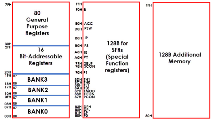
Fig. Lower 128B(00H to 07H) Upper 128B(80H-FFH)
(Direct and Indirect Addressing) (Direct Addressing) (Indirect Addressing)
▪ The 4 banks are named as Bank0, Bank1, Bank2 and Bank3. Each Bank consists of 8 registers R0 – R7. Each Register can be addressed either by name or by address.
▪ To address the register by name, first the corresponding bank is selected. In order to select the bank, RS0 and RS1 bits of the Program Status Word (PSW) and Register (RS0 and RS1 are 3rd and 4th bits in the PSW Register) are used.
▪ When addressing these Register for example 12H the corresponding bank may or may not be selected. (12H corresponds to R2 in Bank2).
▪ The next 16B of the RAM that is from 20H to 2FH are Bit – Addressable memory locations. A total of 128 bits can be addressed individually using 00H to 7FH or an entire byte can be addressed as 20H to 2FH.
▪ The final 80B of the internal RAM addresses are from 30H to 7FH which is the general-purpose RAM area that is byte addressable.
▪ These lower 128B of RAM can be addressed directly or indirectly.
References:
- 8051 Microcontroller: An Applications Based Introduction Book by David Calcutta, Frederick J. Cowan, and Hassan Parchizadeh
- 8051 Microcontrollers: Internals, Instructions, Programming, and Interfacing Book by Subrata Ghoshal
- C and the 8051: Building efficient applications Book by Thomas W. Schultz
- MICROCONTROLLER Book by V. Udayashankara
- The 8051/8052 Microcontroller: Architecture, Assembly Language, and Hardware Interfacing Book by Craig Steiner