Unit - 5
Memory and I/O Interfacing
The 8051 Microcontroller Memory is separated into Program Memory (ROM) and Data Memory (RAM). The Program Memory of the 8051 Microcontroller is used for storing the program to be executed, which means instructions. The Data Memory is used for storing temporary variable data and intermediate results.
Program Memory (ROM) of 8051
The code or instructions which are to be executed are stored in the Program Memory, also called as the ROM of the Microcontroller.
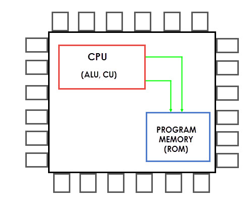
Fig 1. Program Memory
In 4KB Internal ROM, the address space is 0000H to 0FFFH. If the program addresses exceed this value, the CPU will automatically fetch the code from the external Program Memory.
For External Access (EA Pin) must be pulled HIGH at this condition the CPU first fetches instructions from the Internal Program Memory in the address range of 0000H to 0FFFFH .If it exceeds the memory addresses limit, instructions are fetched from external ROM in address range of 1000H to FFFFH.
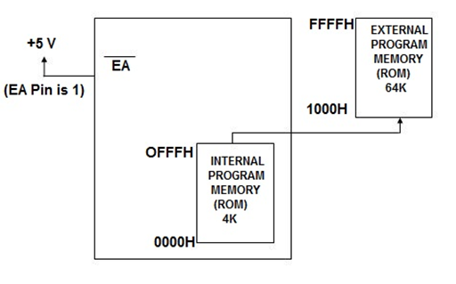
Fig 2. External access
There is also an alternative method to fetch the instructions where the Internal ROM is ignored and instructions are fetched only from External Program Memory(External ROM).
For this purpose, the EA pin must be connected to GND. The memory addresses of external ROM will be from 0000H to FFFFH.
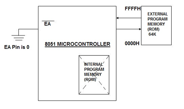
Fig 3. External Program Memory
Data Memory (RAM)
▪ Data Memory or RAM stores temporary data and intermediate results generated during the normal operation of the microcontroller.
▪ Currently, 8051 Microcontroller has 256B of RAM. The first 128B memory addresses from 00H to 7FH are divided into Working Registers. They are organized as Register Banks, Bit – Addressable Area and General Purpose RAM known as Scratchpad area.
▪ The first 128B of RAM (from 00H to 7FH), the first 32B of memory from addresses 00H to 1FH consists of 32 Working Registers organized into four banks with 8 Registers in each Bank.
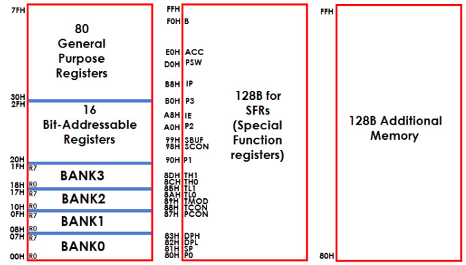
Fig 4. Lower 128B(00H to 07H) Upper 128B(80H-FFH)
(Direct and Indirect Addressing) (Direct Addressing) (Indirect Addressing)
▪ The 4 banks are named as Bank0, Bank1, Bank2 and Bank3. Each Bank consists of 8 registers R0 – R7. Each Register can be addressed either by name or by address.
▪ To address the register by name, first the corresponding bank is selected. In order to select the bank, RS0 and RS1 bits of the Program Status Word (PSW) and Register (RS0 and RS1 are 3rd and 4th bits in the PSW Register) are used.
▪ When addressing these Register for example 12H the corresponding bank may or may not be selected. (12H corresponds to R2 in Bank2).
▪ The next 16B of the RAM that is from 20H to 2FH are Bit – Addressable memory locations. A total of 128 bits can be addressed individually using 00H to 7FH or an entire byte can be addressed as 20H to 2FH.
▪ The final 80B of the internal RAM addresses are from 30H to 7FH which is the general-purpose RAM area that is byte addressable.
▪ These lower 128B of RAM can be addressed directly or indirectly.
I/O Expansion buses:
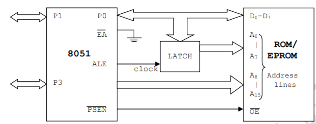
The above figure shows how to access or interface ROM to 8051.
Port 0 is used as multiplexed data & address lines. It gives lower order (A7-A0) 8 bit address in initial T cycle & higher order (A8-A15) used as data bus.
8- bit address is latched using external latch & ALE signal from 8051.
Port 2 provides higher order (A15-A8) 8 bit address.
PSEN is used to activate the output enable signal of external ROM/EPROM.
Ii. External RAM (data memory) Interfacing
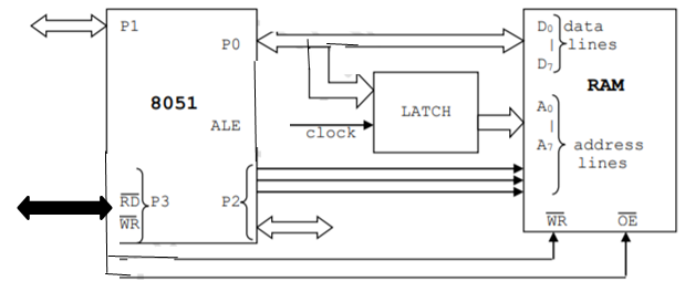
The above figure shows how to connect or interface external RAM(data memory) to 8051. Port 0 is used as multiplexed data & address lines. Address lines are decoded using external latch & ALE signal from 8051 to provide lower order (A7-A0) address lines. Port 2 gives higher order address lines. RD & WR signals from 8051 select the memory read & memory write operations respectively.
Control Signals
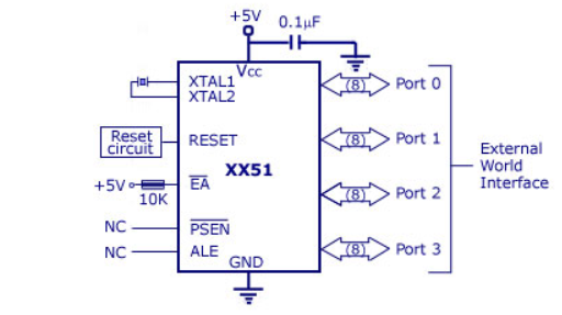
There are 3 control signals, EA, PSEN and ALE. These signals are known as External Access (EA), Program Store Enable (PSEN), and Address Latch Enable (ALE) which is used for external memory interfacing.
The control signals are used for external memory interfacing. If there is no requirement of external memory interfacing then, EA pin is pulled high, that is it is connected to Vcc and two others PSEN and ALE are left alone. To avoid HF oscillations 0.1 micro farad decoupling capacitor connected to Vcc at the input.
There are four ports numbered 0,1,2,3 and called as Port 0, Port 1, Port 2 and Port 3 which are used for external interfacing of devices like DAC, ADC, 7 segment display, LED etc. Each port has 8 I/O lines which are bit programmable.
Memory wait states.
● Program Memory Wait States
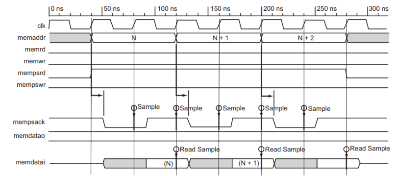
Fig 5. Program Fetch Cycle with wait state
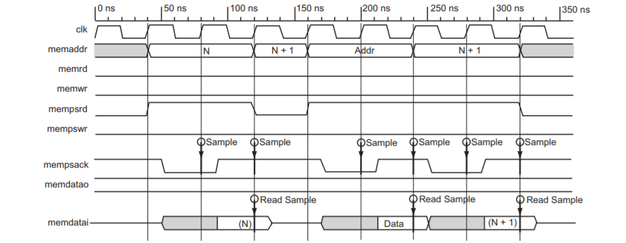
Fig 6. Program Memory Read cycle with wait state
Interfacing is one of the important concepts in microcontroller 8051 because a microcontroller is a CPU that can perform some operation on the data and gives the output.
However, to perform the operation we need an input device to enter the data and in turn output device displays the results of the operation.
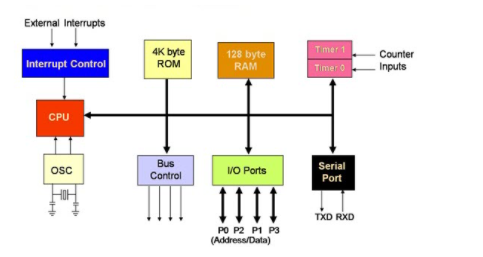
Fig 7. Microcontroller Peripherals Devices
Interfacing is the process of connecting devices together so that they can exchange the information and that proves to be easier to write the programs.
There are different type of input and output devices for our requirement such as LEDs, LCDs, 7segment, keypad, motors and other devices.
ADC0808/0809:
ADC0808/0809 is a monolithic CMOS device which consists of 28 pins and gives 8-bit value in output for 8- channel ADC input pins (IN0-IN7).
It has a resolution of 8 therefore it can encode the analog data into one of the 256 levels (28).
It has three channel address lines namely: ADDA, ADDB and ADDC to select channels.
Pin Diagram for ADC0808
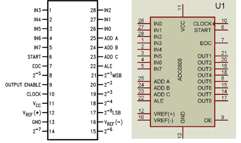
Figure 8. ADC 0808 Pin
ADC0808/0809 needs a clock pulse for conversion which can be provided by using an oscillator or microcontroller.
Select the input channel using address lines, like the input line IN0 by keeping all three address lines (ADDA, ADDB,ADDC) low.
Suppose IN2 is selected to keep ADDA and ADDB low and ADDC high.
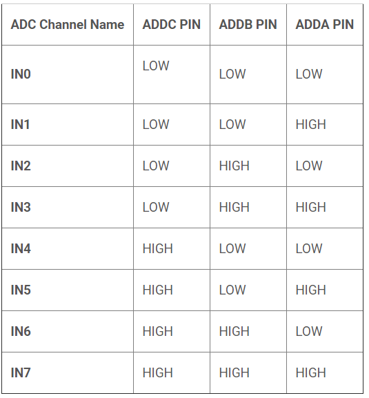
Figure 9. Channel selection
SOC [Start of conversion]:
When High to low signal is appears on the pin of ADC, and ADC starts conversion

Figure 10. SOC
EOC [End of conversion]:
To indicate completion of conversion ADC sends a high EOC signal to the microcontroller.
OE [Output Enable]:
When a high signal is applied to this pin, the output latch of ADC is enabled and the converted data is made available to the Microcontroller.
The reference voltage determines the range of analog input voltage.
For example: - If reference voltage is 5V then analog voltage ranges from 0V-5V. If the reference voltage is 2.56V then the range is from 0V-2.56V.
The frequency of the applied clock signal determines conversion speed.
Working:
⮚ Initially, microcontroller provides a 500 KHz clock signal to ADC0808 because the Timer 0 interrupt requires clock signal to operate to operate as ADC.
⮚ Then the microcontroller sends a LOW to HIGH level signal to ALE pin (active-high pin) of ADC0808 to enable the latch in the address.
⮚ By applying HIGH to LOW Level signal to SC (Start Conversion), ADC starts analog to digital conversion. And then wait for the EOC (End of Conversion) pin to go LOW.
⮚ When EOC goes LOW, it means analog to digital conversion has been completed and data is ready to use.
⮚ After this, the microcontroller enables the output line by applying a HIGH to LOW signal to the OE pin of ADC0808.
⮚ ADC0808 gives ratio metric conversion output at its output pins.
Radiometric conversion is given by
Vin/(Vfs – Vz) = Dx / (Dmax – Dmin)
Where:
Vin is input voltage for conversion
Vfs is full scale voltage
Vz is zero voltage
Dx is data point being measured
Dmax is maximum data limit
Dmin is the minimum data limit.
Interfacing Diagram:
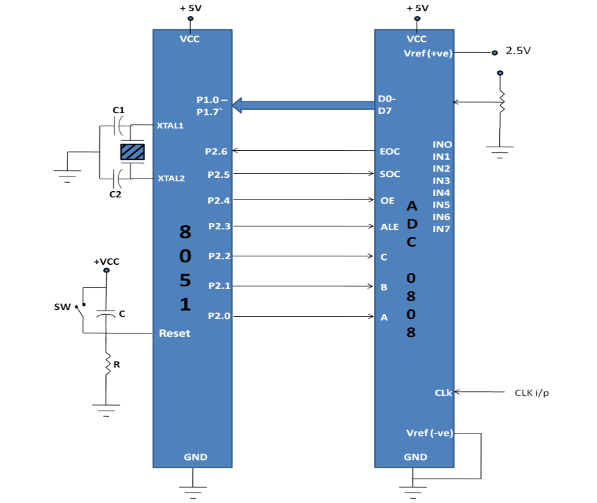
Figure 11. Interfacing 8051 with ADC0808
Program:
SOC EQU P2.6
EOC EQU P2.5
OE EQU P2.4
ALE EQU P2.3
ADDR_C EQU P2.2
ADDR_B EQU P2.1
ADDR_A EQU P2.0
ORG 0000H
MOV P1, #0FFH
SETB P2.5
CLR SOC
CLR OE
CLR ALE
AGAIN: CLR ADDR_C
CLR ADDR_B
CLR ADDR_A
SETB SOC
SET ALE
ACALL DELAY
CLR SOC
CLR ALE
BACK: JB EOC BACK
HERE: JNB EOC HERE
SETB OE
MOV A,P1
ACALL CONVERSION
ACALL DISPLAY
AGAIN: SJMP AGAIN
The Digital to Analog converter (DAC) is a device used for converting digital pulses to analog signals.
There are two methods of converting digital signals to analog signals which are inary weighted method and R/2R ladder method.
The MC1408 (DAC0808) Digital to Analog Converter uses the R/2R ladder method. This method can achieve a higher degree of precision. DACs are judged by its resolution., If there are n digital input pins, there are 2n analog levels. So, 8 input DAC has 256 discrete voltage levels.
MC1408 DAC (or DAC0808)
In this chip the digital inputs are converted to current. The output current is known as Iout by connecting a resistor to the output to convert into voltage.
The total current provided by Iout pin is basically a function of binary numbers at the input pins D0 - D7 (D0 is the LSB and D7 is the MSB) of DAC0808 and the reference current Iref.
The following formula is showing the function of Iout
Iout=Iref⟮D7/2+D6/4+D5/8+D4/16+D3/32+D2/64+D1/128+D0/256⟯
The Iref is the input current. This must be provided into the pin 14. Generally 2.0mA is used as Iref
Generating Sinewave using DAC and 8051 Microcontroller
For generating sinewave first we need a look-up table to represent the magnitude of the sine value of angles between 0° to 360°. The sine function varies from -1 to +1.
In the table only integer values are applicable for DAC input. In this example we will consider 30° increments and calculate the values from degree to DAC input. We are assuming a full-scale voltage of 10V for DAC output.
We can follow this formula to get the voltage ranges.
Vout = 5V + (5 x sin θ)
The lookup table according to the angle and other parameters for DAC.
Angle(in θ ) | Sinθ | Vout (Voltage Magnitude) | Values sent to DAC |
0 | 0 | 5 | 128 |
30 | 0.5 | 7.5 | 192 |
60 | 0.866 | 0.866 | 9.33 |
90 | 1.0 | 1.0 | 10 |
120 | 0.866 | 0.866 | 9.33 |
150 | 0.5 | 0.5 | 7.5 |
180 | 0 | 0 | 5 |
210 | -0.5 | -0.5 | 2.5 |
240 | -0.866 | -0.866 | 0.669 |
270 | -1.0 | -1.0 | 0 |
300 | -0.866 | -0.866 | 0.669 |
330 | -0.5 | -0.5 | 2.5 |
360 | 0 | 0 | 5 |
Angle(in θ ) | Sinθ | Vout (Voltage Magnitude) | Values sent to DAC |
0 | 0 | 5 | 128 |
30 | 0.5 | 7.5 | 192 |
60 | 0.866 | 9.33 | 238 |
90 | 1.0 | 10 | 255 |
120 | 0.866 | 9.33 | 238 |
150 | 0.5 | 7.5 | 192 |
180 | 0 | 5 | 128 |
210 | -0.5 | 2.5 | 64 |
240 | -0.866 | 0.669 | 17 |
270 | -1.0 | 0 | 0 |
300 | -0.866 | 0.669 | 17 |
330 | -0.5 | 2.5 | 64 |
360 | 0 | 5 | 128 |
Circuit Diagram −
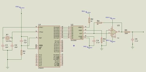
Source Code
#include <reg51.h>
Sfr DAC = 0x80; // Port P0 address
Void main()
{
Int sin value[12] = {128,192,238,255,238,192,128,64,17,0,17,64};
Int i;
While(1){
// infinite loop for LED blinking
For(i=0;i<12;i++)
{
DAC = sin_value[i];
}
}
}
Output
The output will look like this −
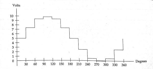
The 8051 has two timers: timer0 and timer1. Both timers are 16 bits wide. Since the 8051 has an 8-bit architecture, each 16-bit is accessed as two separate registers of low byte and high byte.
Timer0 registers is a 16- bits register which is accessed as low byte and high byte. The low byte is TL0 and the high byte is TH0.
These registers are accessed like any other registers where the 16-bits register is accessed as low byte and high byte. The low byte is TL0 and the high byte is TH0.

Fig 12. Timer 0
Timer1 registers is also a 16- bit register and is split into two bytes referred to as TL1 and TH1.

Fig 13. Timer 1
TMOD (timer mode) Register: This is an 8-bit register which is used by both timers 0 and 1 to set the various timer modes. In this TMOD register, lower 4 bits are set aside for timer0 and the upper 4 bits are for timer1. The lower 2 bits are used to set the timer mode and upper 2 bits to specify the operation.

In upper or lower 4 bits, the first bit is a GATE bit. Every timer has a means of starting and stopping. Some timers do this by software, some by hardware, and some have both software and hardware controls. The hardware way of starting and stopping the timer by an external source is achieved by making GATE=1 in the TMOD register. And if we change to GATE=0 then we do not need external hardware to start and stop the timers.
The second bit is the C/T bit which is used to decide whether a timer is used as a time delay generator or an event counter. If this bit is 0 then it is used as a timer and if it is 1 then it is used as a counter.
In upper or lower 4 bits, the last bits third and fourth are known as M1 and M0 respectively. These are used to select the timer mode.
M0 | M1 | Mode | Operating Mode |
0 | 0 | 0 | 13-bit timer mode, 8-bit timer/counter THx and TLx as 5-bit prescalar. |
0 | 1 | 1 | 16-bit timer mode, 16-bit timer/counters THx and TLx are cascaded; There are no prescalar. |
1 | 0 | 2 | 8-bit auto reload mode, 8-bit auto reload timer/counter; THx holds a value which is to be reloaded into TLx each time it overflows.
|
1 | 1 | 3 | Split timer mode.
|
Mode 1- It is a 16-bit timer which allows values from 0000 to FFFFH to be loaded into the timer’s registers TL and TH. After TH and TL are loaded with 16-bit initial value, the timer is started.
“SETB TR0” for timer 0 and “SETB TR1” for timer 1.
After the timer is started. It starts counting up until it reaches its limit of FFFFH. When it rolls over from FFFF to 0000H, it sets a high flag bit called TF (timer flag). This timer flag can be monitored.
When this timer flag is raised, one option is to stop the timer with the instructions “CLR TR0” or CLR TR1 for timer 0 and timer 1 respectively. After the timer reaches its limit and rolls over to repeat the process the registers TH and TL must be reloaded with the original value and TF must be reset to 0.
Mode0- Mode 0 is exactly the same as mode 1 except that it is a 13-bit timer instead of 16-bit. The 13-bit counter can hold values between 0000 to 1FFFH in TH-TL. Therefore, when the timer reaches its maximum of 1FFH, it rolls over to 0000, and TF is raised.
Mode 2- It is 8- bit timer that allows only values of 00 to FFH to be loaded into the timer’s register TH. After TH is loaded with 8- bit value 8051 gives a copy of it to TL. Then the timer must be started.
The instruction “SETB TR0” for timer 0 and “SETB TR1” for timer1.
This is like mode 1. After the timer is started it starts to count up by incrementing the TL register. It counts till it reaches the limit of FFH.
When it rolls over from FFH to 00. It sets high the TF (timer flag).
If we are using timer 0, TF0 goes high;
If using TF1 then TF1 is raised.
When Tl register rolls from FFH to 00 and TF is set to 1, TL is reloaded automatically with the original value kept by the TH register. To repeat the process, clear TF .This makes mode 2 auto reload, in contrast to mode 1 in which the programmer has to reload TH and TL.
Mode3- Mode 3 is also known as a split timer mode. Timer 0 and 1 may be programmed to be in mode 0, 1 and 2 independently of similar mode for other timer. This is not true for mode 3; timers do not operate independently if mode 3 is chosen for timer 0. Placing timer 1 in mode 3 causes it to stop counting; the control bit TR1 and the timer 1 flag TF1 are then used by timer0.
Internal Program Memory (4KB) 0000H to 0FFFH
External Program Memory (60KB) from 1000H to FFFFH.
We can select this mode by making EA = 1.
Total External Program Memory (64KB) that is over the entire range of 0000H to FFFFH. We can select this mode by making EA = 0.
The external storage is addressed and accessed via I/O ports P0 and P2. In 8051, the PSEN = 1 (is active) when reading a byte from external program memory (ROM).
The command used to access external ROM is,
MOVC A, @A+DPTR
When we connect PSEN to the ground, then 8051 microcontroller fetches the opcode from the external ROM.
But, when we connect PSEN to VCC, the status of the PSEN is ‘not activated’ since it is an active low pin. Hence, the program memory is saved in the internal ROM of 8051 itself.
Circuit diagram to interface external program ROM with 8051
Step 1: Connect EA pin to ground
Step 2: Connect the PSEN to the CE and OE.
Step 3: Then, Port 2 (P2.0 – P2.7) to A8 – A12 pins of ext. ROM.
Step 4: Connect ALE to G of 74LS373 latch to enable it.
Step 5: Next, connect the OC of 74LS373 to GND.
Step 6: Connect Port 0 (P0.0 – P0.7), which consists of both address and data multiplexed into Port 0 to 1D – 8D pins of 74LS373 latch to demultiplex it and 1Q – 8Q of the latch to A0 – A7 of ext. ROM.
Step 7: Connect Port 0 (P0.0 – P0.7) to D0 – D7 of the ext. ROM.
Step 8: VPP of ext. ROM to VCC.
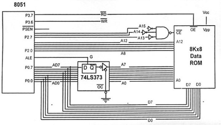
Here, 8Kx8 means that program ROM is organized in a structure that has an 8K word space and the x8 means that each word is 8 bits. This means that 32Kx8 would be a ROM which has a 32K word space, at 8-bits per word. In other words, this means that there are 32,000 locations that are 8-bit wide.
The Program and Data Memory can be of the size 1Kx8, 2Kx8, 4Kx8, 8Kx8, 16Kx8, 32Kx8, and 64Kx8. Also, multiple chips of smaller sizes cascade together to form a chip of larger size hence we can connect two 16Kx8 data RAM chips to form one 32Kx8 data RAM. If we take 32Kx8, then 2^15 = 32K, which implies 15 address lines and x8 implies 8 data lines.
The fastest way of transmitting data within a microcomputer is parallel data transfer.
• For transferring data over long distances parallel data transmission requires too many wires.
• For long distance transmission the data is usually converted from parallel form to serial form so that it can be sent on a single wire or pair of wires.
• Serial data received from a distant source is converted to parallel form which can be easily transferred on the microcomputer buses.
• The types of communication systems are:
1. Simplex
2. Half-duplex
3. Full-duplex
In simplex communication the data can be transmitted only in one direction, that is data from sensors to processor.
Eg: commercial radio stations.
In half-duplex transmission, data can be transmitted in either direction between two systems but can occur only in one direction at a time.
Eg: two-way radio system, where one user always listens while the other talks because the receiver circuitry is turned off during transmit.
In full duplex, the data can be sent and received at the same time.
Eg: A normal phone conversation.
Serial data can be sent in two ways.
They are, 1. Synchronous communication
2. Asynchronous communication
In synchronous transmission the data is transmitted in blocks at a constant rate. The start and end of a block are identified with specific bytes or bit patterns. In asynchronous transmission, data is transmitted one by one. The beginning of a data character is indicated by the line going low for 1- bit time. This bit is called a start bit.
The data bits are then sent out on the line one after the other.
Depending on the system, the data word may consist of 5, 6, 7 or 8 bits. Following the data bits is a parity bit, which is used to check for errors in received data. The line is returned high for at least 1-bit time to identify the end of the character. This always-high bit is referred to as a stop bit. Some systems may use 2 stop bits. The bit format for asynchronous data transmission is
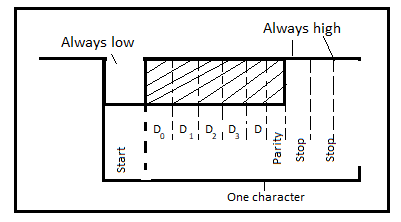
The term baud rate is used to indicate the rate at which serial data is being transferred. Baud rate = 1/ time for a bit cell
• A device such as INTEL 8251A can be programmed to do either asynchronous or synchronous communication, is often called USART (Universal Synchronous Asynchronous Receiver Transmitter).
RS-232C serial data standard:
• In serial I/O, data can be transmitted as either current or voltage.
• When data is transmitted as voltage, the commonly used standard is known as RS-232C.
• This standard proposes a maximum of 25 signals for the bus used for serial data transfer.
• The 25 signals of RS-232C are
Pin number | Common name | RS-232C Name | Description | Signal Direction on DCE |
1 | - | AA | Protective ground | - |
2 | TxD |
|
|
|
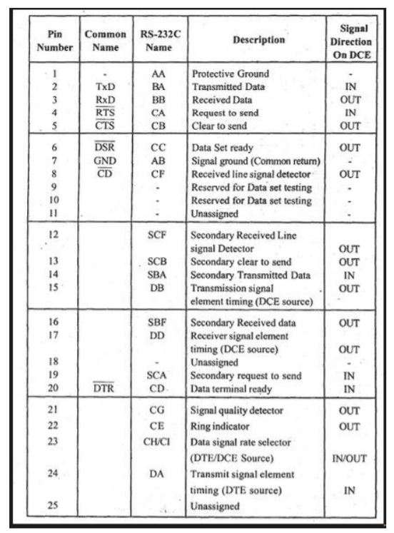
In practice the first 9-signals are sufficient for most of the serial data transmission scheme and so the RS-232C bus signals are terminated on a D-type 9- pin connector. • When all the 25 signals are used, then the RS-232C serial bus is terminated on a 25-pin connector.
- Serial Peripheral Interface (SPI) is an interface bus used to send data between microcontrollers and small peripherals such as shift registers, sensors, and SD cards. It uses separate clock and data lines, along with a select line to choose the device to talk to.
- SPI has a "synchronous" data bus, which means that it uses separate lines for data and a "clock" that keeps both sides in perfect sync.
- The clock is an oscillating signal which tells the receiver exactly when to sample the bits on the data line. This could be the rising (low to high) or falling (high to low) edge of the clock signal. When the receiver detects that edge, it will immediately look at the data line to read the next bit. Because the clock is sent along with the data.
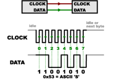
Fig 14. SPI
In SPI, only one side generates the clock signal called SCK for Serial ClocK. The side that generates the clock is called the "master", and the other side is called the "slave". There is always only one master, but there can be multiple slaves.
When data is sent from the master to a slave, it's sent on a data line called MOSI, for "Master Out / Slave In". If the slave needs to send a response back to the master, the master will continue to generate a prearranged number of clock cycles, and the slave will put the data onto a third data line called MISO, for "Master In / Slave Out".
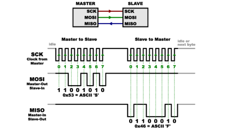
Fig 15. Master-Slave
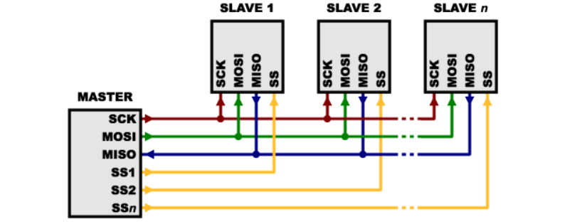 Fig 16. Multiple Slave
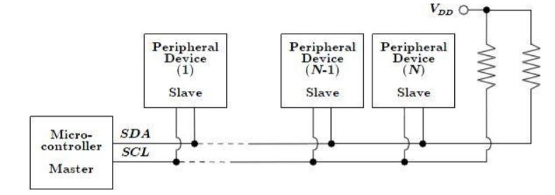
I2C is a multi-point protocol in which peripheral devices are able to communicate along the serial interface which is composed of a bidirectional serial data line (SDA) and a bidirectional serial clock (SCL).
The electrical interconnection beyond the wires is a single 4.7 kilo ohm pull-up resistor for each of the I2C bus lines. Consequently, a slave device writing to SDA needs to pull the line low for each ‘0’written; otherwise, it leaves the line alone to write a ‘1’, which occurs due to the lines being pulled high externally by the pull-up resistor. This is commonly known as a wired-AND configuration
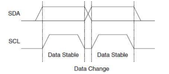
Transferring Bits on the I2C bus is accompanied by a pulse on the clock (SCL) line. The level of the data line must be stable when the clock line is high. The only exception to this rule is for generating start and stop conditions.
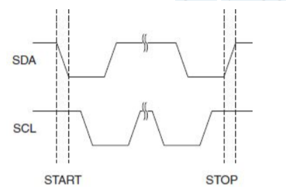
START and STOP conditions are signaled by changing the level of the SDA line when the SCL line is high.
All packets transmitted on the I2C bus are 9 bits long. An address packet consists of 7 address bits (27 = 128 possible addresses), one READ/WRITE control bit and an acknowledge bit. An address packet consisting of a SLave Address and a READ or a WRITE bit is called SLA+R or SLA+W, respectively. A data packet consists of one data byte and an acknowledge bit.

The master begins communication by transmitting a single start bit followed by the unique 7-bit address of the slave device for which the master is attempting to access, followed by a read/write bit.
The corresponding slave device responds with an acknowledge bit if it is present on the serial bus.
The master continues to issue clock events on the SCL line and either receives information from the slave or writes information to the slave depending on the read/write bit at the start of the session.
The number of bits transferred during a single session is dependent upon the peripheral device and the agreed-upon higher-level protocol.
ZigBee is a specification for high- level communication protocols using small low-power digital radios based on IEEE -802 standard for personal area networks.
Figure shows how to interface the Zigbee with a microcontroller.
The Xbee modules work at the 2.4 GHz frequency which means smaller board and antenna size.
Xbee modules can transmit Digital, PWM, Analog or Serial RS232 signals wirelessly.
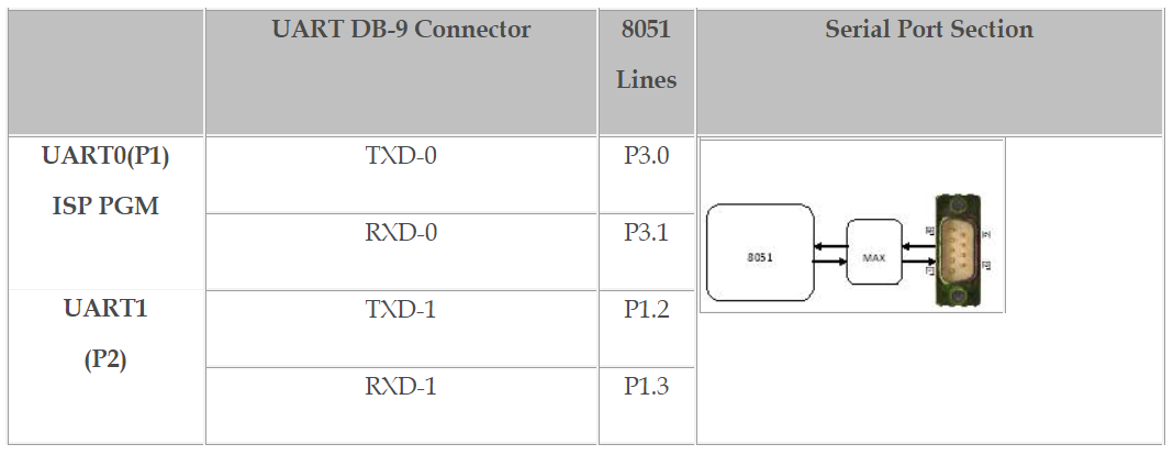
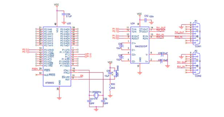
To communicate over UART or USART, three basic signals namely, RXD (receive), TXD (transmit), GND (common ground) are used to interface UART with 8051.
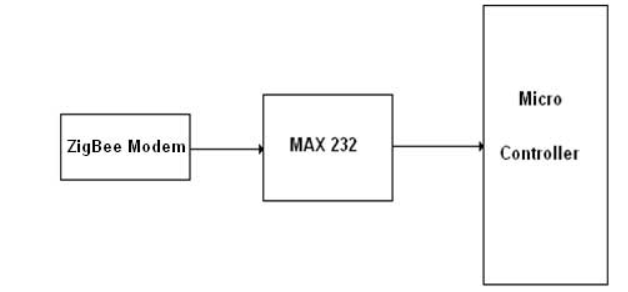
Pin Assignment with 8051
#include //Define 8051 Registers
Void serial(void); //Serial Communication Register
Void DelayMs(unsigned int); //Delay Function
Unsigned int i,j;
Unsigned char b[25],d;
//---------------------------
// Main Program
//---------------------------
Void main()
{
EA=1; //Enable All Interrupt
ES=1; //Enable Serial Port Interrupt
Serial(); //Serial Communication
While(1); //Loop Forever
}
//------------------------------------------
// Serial Communication Register Initialisation
//------------------------------------------
Void serial(void)
{
TMOD=0X20; //Timer1, Mode2
SCON=0X50; //Serial Mode1, Receive Enable
TH1=0XFD; //Baud Rate 9600bps
TR1=1; //Timer1 ON
}
//-----------------------------------------
// Serial Interrupt Function
//-----------------------------------------
Void serin (void) interrupt 4 //Serial Port Interrupt
{
If(RI==1) //Receive Interrupt Gets Enabled
{ //after Stop Bit get Received
d=SBUF; //Serial Buffer value moved to a variable
b[j]=d;
SBUF=b[j];
DelayMs(20); //Delay Function
j++;
}
SCON=0X50; //Initialising Receive and Transmit Interrupt
}
//---------------------------------
// Delay Function
//---------------------------------
Void DelayMs(unsigned int k)
{
Unsigned int i;
For(i=0;i<=k;i++);
}
Bluetooth
The HC-05 Bluetooth Module is an easy-to-use Bluetooth serial module. It is designed for transparent wireless serial connection setup. Its communication is through serial mode which makes it easy to interface with any microcontroller.
The HC-05 Bluetooth module provides a switching mode between master and slave mode. A single master device can be connected to up to several different slave devices. But, a slave device in the Bluetooth network can only be connected to a single master. The master device can send data to any of its slaves and request data from them as well, but the slaves are only allowed to transmit to and receive from their master.
The HC-05 Bluetooth module can be configured as a master device or a slave device with the help of AT.
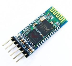
To enable Bluetooth communication, the HC-05 module is interfaced with the 8051 microcontroller via the built-in UART circuitry present in the microcontroller. And the data is transmitted in the form of packets. The 8051 microcontrollers have inbuilt pins P3.0 (RXD) and P3.1 (TXD) for receiving and transmitting the data from/to the HC-05 Bluetooth module respectively.
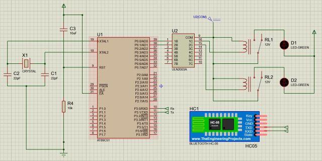
Circuit diagram to interface Bluetooth module and relay with 8051
● Step 1: If you are using Proteus or other simulation software or even hardware, select the AT89C51 or AT89S51 microcontroller.
● Step 2: Connect a 12 MHz oscillator between pin 18 and 19.
● Step 3: Connect two capacitors of 22pF, with one terminal on either side of the oscillator and the other terminal to ground, as shown below.
● Step 4: Set Pin 31,EA pin to HIGH by connecting it to the +5V DC source.
● Step 5: To make the RESET circuit, connect Pin 9 (RST) to +5V through a capacitor of 10µF and connect the same pin to +0V (GND) through a 10kΩ resistor or a potentiometer.
● Step 6: Connect two LEDs to the microcontroller such that they turn ON when a low pulse is given through Port 0’s output. For this, ULN2003a driver is used, pin P0.0 and P0.1 are connected to 1B and 2B of ULN2003A, respectively.
● Step 7: The output pins 1C and 2C of ULN2003a are given to one terminal of the coil of the relay and the other terminal of the coil of the relay is connected to the COM pin of ULN2003A which is connected to a DC supply.
● Step 8: One side of the contactor of the relay is connected to the cathode of the LED, and the anode is connected to the power supply. Connect the other side of the contactor to the COM pin of ULN2003A.
● Step 9: Connect the RXD (P3.0) and TXD (P3.1) of the 8051 microcontrollers to TXD and RXD pins of HC-05 Bluetooth module respectively.
● Step 10: VCC and GND pins of the HC-05 Bluetooth module are to be given to +5V/3.3V and GND, respectively, for the module to turn ON.
#include<reg51.h>
#include<stdio.h>
Sbit LED1 = P0^0; //Assign LED1 to pin P0.0
Sbit LED2 = P0^1; //Assign LED2 to pin P0.1
Void main()
{
Char mychar; // Assign a variable for the character to be received
TMOD = 0x20; // Set time Timer 1 in 8-bit auto-reload mode (mode 2)
TH1 = 0xFD; // FD = -3, to send/ receive the data at 9.6Kbps
SCON = 0x50; // Serial Control is set in Mode 1, with REN = 1 (reception ON)
TI = 0; // Initialize the Timer Flag
RI = 0; // Initialize the Timer
TR1 = 1; // Start the timer (Timer 1)
While(1) // Runs forever until power supply is cut off
{
While (RI == 0); // Wait till the data is received, as soon as the data is received completely, the RI flag is set
RI = 0; // Clear the RI flag to declare the availability for reception of another data
If (mychar == 'A') // If the data received through the Bluetooth module is the character 'A'
{
LED1 = 0; // Turn ON LED 1
}
Else if (mychar == 'a') // If the data received through the Bluetooth module is the character 'a'
{
LED1 = 1; // Turn OFF LED 1
}
If (mychar == 'B') // If the data received through the Bluetooth module is the character 'B'
{
LED2 = 0; // Turn ON LED 2
}
Else if (mychar == 'b') // If the data received through the Bluetooth module is the character 'b'
{
LED2 = 1; // Turn OFF LED 2
}
}
}
References:
- 8051 Microcontroller: An Applications Based Introduction Book by David Calcutt, Frederick J. Cowan, and Hassan Parchizadeh
- 8051 Microcontrollers: Internals, Instructions, Programming, and Interfacing Book by Subrata Ghoshal
- C and the 8051: Building efficient applications Book by Thomas W. Schultz
- MICROCONTROLLER Book by V. Udayashankara
- The 8051/8052 Microcontroller: Architecture, Assembly Language, and Hardware Interfacing Book by Craig Steiner