Unit - 3
DC-DC Buck and Boost Converter
A chopper is a DC equivalent to an AC transformer having continuously variable turn ratio. Like a transformer, a it can be used to step up or step down the fixed DC input voltage. On this basis, there are two types of chopper: Step-up and Step-down Chopper. A chopper whose average value of DC output voltage is more than the fixed DC input voltage is called Step-up Chopper. While, a chopper whose average value of DC output voltage is less than the DC input voltage is called Step-down chopper.
Working Principle of Chopper:
A chopper is a high speed ON/OFF switch. It connected source to load and disconnects the load from the source at a fast speed. Figure below represents the simple circuit to show its working principle.
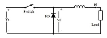
Figure 1. Chopper
In this circuit, the switch SW is chopper. This switch can be made ON and OFF at a very high speed. In this way, the load may be connected and disconnected from the supply source Vs. When the switch is ON, the load voltage is equal to the source voltage Vs and when the switch is OFF, load voltage becomes equal to ZERO. Thus, a chopped voltage across the load is obtained. The output voltage i.e. voltage across the load is shown in figure below.
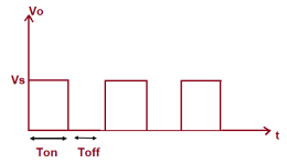
Figure 2. Output waveforms
It should be noted here that, when the switch SW is made OFF, the load current finds its path through free- wheeling diode D. Therefore, diode D acts as a short and hence the voltage across the load becomes zero. Inductor in the chopper is an essential thing. This inductor makes diode D forward biased when the switch SW is OFF.
It should also be noted that, even though the switch SW is made OFF, the load current doesn’t become zero. Rather, it flows through the free- wheeling diode, inductor L and load. In fact, the load current is continuous as shown below.
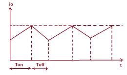
Figure 3. Load current
It may be seen from the above waveform of output current of chopper that, during ON time, the current rises whereas during OFF time, the load current io decays.
The time for which chopper connects the load from source is called ON time i.e. TON. Whereas, the time for which load is disconnects from source is called OFF time i.e. TOFF.
Duty Cycle:
Duty cycle of chopper is defined as the ratio of ON time to the total time period. It is denoted by symbol α. Total time period is the sum of ON and OFF time.
Duty Cycle = TON / (TON+TOFF)
Assuming (TON+TOFF) = T, duty cycle is given as below.
Duty Cycle, α = (TON / T)
Calculation of Output Voltage:
The average output voltage of chopper may be find from the output voltage waveform. It is clear from the o/p voltage waveform that, voltage Vo is available only for TON time period in the total time (TON+TOFF). Therefore, average output voltage Vo may be calculated as shown below.
Vo = TON Vs / (TON+TOFF)
But, TON / (TON+TOFF) = α
Hence,
Vo = αVs
Thus, the output voltage may be controlled by controlling the duty cycle. This duty cycle may be controlled in various ways which we will discuss in the next post. From the expression of ouput voltage, it is also clear that, the output voltage is independent of the load current.
The expression for chopper output voltage may also be written as below.
Vo = TON Vs / (TON+TOFF)
= Vs TON / T
Assuming 1/T = Chopping frequency
Vo = f Vs TON.
Class A Chopper
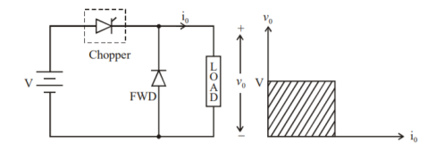
Figure 4 (a) Class A chopper
Figure shows a Class A Chopper circuit with inductive load and free-wheeling diode. When chopper is ON, supply voltage V is connected across the load that is current i0 flows as shown in figure.
When chopper is OFF, v0 = 0 and the load current continues to flow in the same direction through the free -wheeling diode. Therefore, the average values of output voltage and current are always positive. Hence, Class A Chopper is a first quadrant chopper (or single quadrant chopper).
Figure (b) shows output voltage and current waveforms for a continuous load current.
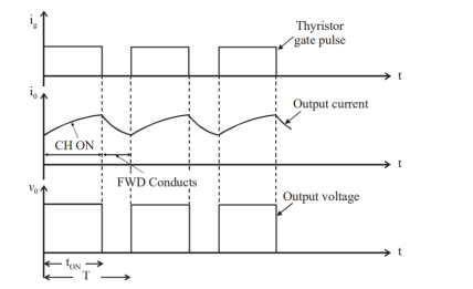
Figure 4 (b) Output voltage and current waveforms.
Class A Chopper is a step-down chopper in which power always flows from source to load. It is used to control the speed of dc motor. The output current equations obtained in step down chopper with R-L load can be used to study the performance of Class A Chopper.
CLASS B CHOPPER
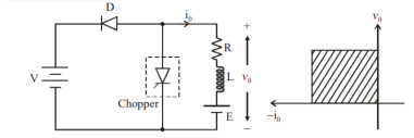
Figure 5 Class B chopper
Fig. Shows a Class B Chopper circuit. When chopper is ON, and E drives a current through L and R in a direction opposite to that shown in figure. During the ON period of the chopper, the inductance L stores energy.
When Chopper is OFF, diode D conducts, and part of the energy stored in inductor L is returned to the supply. Also, the current continues to flow from the load to source. Hence the average output voltage is positive and average output current is negative.
Therefore, Class B Chopper operates in second quadrant. In this chopper, power flows from load to source. Class B Chopper is used for regenerative braking of dc motor.
Figure (b) shows the output voltage and current waveforms of a Class B Chopper. The output current equations can be obtained as follows. During the interval diode ‘D’ conducts (chopper is off) voltage equation is given by
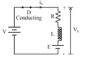

For the initial condition i.e., at. The solution of the above equation is obtained along similar lines as in step-down chopper with R-L load
Therefore 
At 


During the interval chopper is ON voltage equation is given by
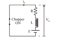

Redefining the time origin, at t=0, 
The solution for the stated initial condition is


Therefore 
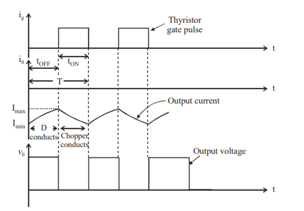
Figure 6. Class B Chopper Output Voltage and current waveform.
CLASS C CHOPPER
Class C Chopper is a combination of Class A and Class B Choppers. Figure a) shows a Class C two quadrant Chopper circuit.
For first quadrant operation, is ON or conducts and for second quadrant operation, is ON or conducts. When is ON, the load current is positive. i.e., flows in the direction as shown in figure
The output voltage is equal to V and the load receives power from the source.
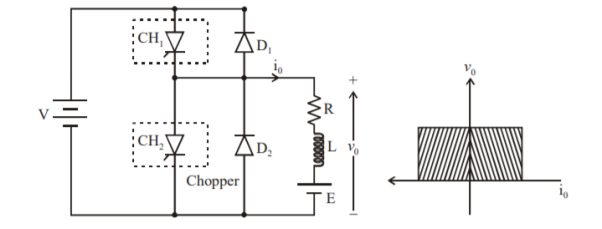
Figure 7. Class C chopper
When CH1 is turned OFF, the energy stored in inductance L forces current to flow through the diode and the output voltage vo=0V, but io continues to flow in positive direction. When CH2 is triggered, the voltage E forces io to flow in opposite direction through L and CH2. The output voltage v0=0.
On turning OFF CH2 the energy stored in the inductance drives current through diode D1 and the supply.
The output voltage v0=V the input current becomes negative and power flows from load to source.
Thus, the average output voltage vo is positive but the average output current io can take both positive and negative values. Choppers CH1 and CH2 should not be turned ON simultaneously as it would result in short circuiting the supply.
Class C Chopper can be used both for dc motor control and regenerative braking of dc motor. Figure shows the output voltage and current waveforms.
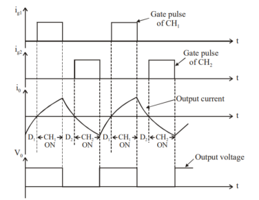
Figure 8. Class C chopper output voltage and current waveform.
Class D chopper
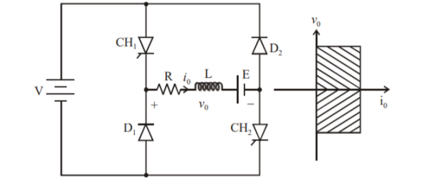
Figure 9. D chopper
Figure shows a class D two quadrant chopper circuit. When both and are triggered simultaneously, the output voltage vo=V and output current Io flows through the load in the direction shown in figure.
When CH1 and CH2 are turned off the load io continues to flow in the same direction through load.
D1 and D2 due to energy stored in inductor L but output voltage vo = -V. The average load voltage vo is positive if chopper ON time (t ON) is more than OFF time t(OFF) and the average output voltage becomes negative if ton<toFF.
Hence, the direction of load current is always positive. But load voltage can be positive or negative.
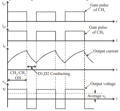
Output voltage for ton>toff
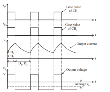
Output voltage for ton<toff
Figure 10. Output waveforms.
Class E chopper:
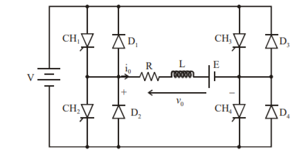
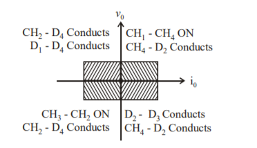
Four Quadrant Operation
Figure 11. Class E chopper
Figure shows a class E 4 quadrant chopper circuit. When they are triggered, output current flows in positive direction as shown in figure through and, with output voltage vo=V. This gives the first quadrant operation.
When both and are OFF, the energy stored in the inductor L drives through and in the same direction, but output voltage vo=-V. Therefore, the chopper operates in the fourth quadrant.
For fourth quadrant operation the direction of battery must be reversed. When Ch2 and Ch3 are triggered, the load current io flows in opposite direction and output voltage vo = -V. Since both io and vo are negative, the chopper operates in third quadrant.
When both CH2 and CH3 are OFF, the load current io continues to flow in the same direction through D1 and D4 and the output voltage vo=V. Therefore, the chopper operates in second quadrant as vo is positive but io is negative. Figure shows the devices which are operative in different quadrants.
Key takeaway
- Class A Chopper is a step-down chopper in which power always flows from source to load. It is used to control the speed of dc motor.
- Therefore, Class B Chopper operates in second quadrant. In this chopper, power flows from load to source. Class B Chopper is used for regenerative braking of dc motor.
- Class C Chopper can be used both for dc motor control and regenerative braking of dc motor. It is the combination of class A and class B chopper.
- Class D chopper can operate in different quadrants.
Solved Examples
Q1) A Chopper circuit is operating on TRC at a frequency of 2 kHz on a 460 V supply. If the load voltage is 350 volts, calculate the conduction period of the thyristor in each cycle.
A1)

Chopping period 

Output voltage 
Conduction period of thyristor


Q2) Input to the step up chopper is 200 V. The output required is 600 V. If the conducting time of thyristor is 200 µsec. Compute – Chopping frequency, – If the pulse width is halved for constant frequency of operation, find the new output voltage.
A2)


Solving for T
T=200s
Chopping frequency 

Pulse width is halved

Frequency is constant 

Output voltage 
Q3) A dc chopper has a resistive load of 20Ω and input voltage VS = 220V. When chopper is ON, its voltage drop is 1.5 volts and chopping frequency is 10 kHz. If the duty cycle is 80%, determine the average output voltage and the chopper on time.
A3) 

 Voltage drops across chopper =1.5 volts
Average output voltage


 Voltage drops across chopper=1.5 volts
Average Output voltage


Chopper ON time 
Chopping period, 

Chopper ON time


Q4) In a dc chopper, the average load current is 30 Amps, chopping frequency is 250 Hz, supply voltage is 110 volts. Calculate the ON and OFF periods of the chopper if the load resistance is 2 ohms.
A4)


 and
and 


Chopper ON period

Chopper OFF period


A typical Buck converter is shown below.

Figure 12. Buck converter
The input voltage source is connected to a controllable solid- state device which operates as a switch. The solid-state device can be a Power MOSFET or IGBT.
The second switch used is a diode. The switch and the diode are connected to a low-pass LC filter which is appropriately designed to reduce the current and voltage ripples. The load is a purely resistive load.
The input voltage is constant and the current through load is also constant. The load can be seen as current source.
The controlled switch is turned on and off by using Pulse Width Modulation(PWM).
PWM can be time based or frequency based.
The Buck converter has two modes of operation. The first mode is when the switch is on and conducting.
Mode I: Switch is ON, Diode is OFF
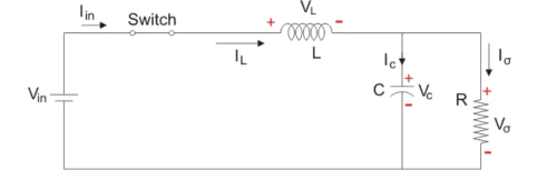
Figure 13. Buck converter circuit(Switch ON)
The voltage across the capacitance in steady state is equal to the output voltage.
Let us say the switch is on for a time TON and is off for a time TOFF. We define the time period, T,
T = TON + T OFF
And the switching frequency
Fswitching = 1/T
Let us now define another term, the duty cycle,
D = TON/T
Let us analyze the Buck converter in steady state operation for this mode using KVL.
Vin = VL + Vo
DiL/dt = ∆ iL/∆t = ∆iL/DT = Vin-Vo/L
Since the switch is closed for a time Ton = DT we can say that ∆t=DT
(∆ iL ) closed= (Vin - Vo/L) DT
While performing the analysis of the Buck converter, we have to keep in mind that
The inductor current is continuous and, this is made possible by selecting an appropriate value of L.
The inductor current in steady state rises from a value with a positive slope to a maximum value during the ON state and then drops back down to the initial value with a negative slope. Therefore the net change of the inductor current over anyone complete cycle is zero.
Mode II: Switch is OFF, Diode is ON
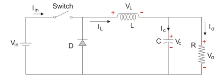
Figure 14. Switch off
Here, the energy stored in the inductor is released and is ultimately dissipated in the load resistance, and this helps to maintain the flow of current through the load. But for analysis we keep the original conventions to analyse the circuit usingKVL.
Let us now analyse the Buck converter in steady state operation for Mode II using KVL.
0 = VL + Vo
VL = L diL/dt = -VO
DiL/dt = ∆ iL/∆t = ∆ iL / (1-D) T = -Vo/L
Since the switch is open for a time
TOFF = T – TON = T -DT = (1-D) T
We can say that
∆t = (1-D) T
(∆ iL) open = ( -Vo/L) (1-D) T
It is already established that the net change of the inductor current over any one complete cycle is zero
(∆ iL) closed + (∆ iL) open =0
(Vin – Vo) /L .DT + (-Vo/L) DT =0
Vo /Vin = 1/ 1-D
Since the switch is open for a time
TOFF = T – TON = T – DT = (1-D) T
We can say that
∆t = (1-D) T
It is already established that the net change of the inductor current over any one complete cycle is zero.
(∆ iL) closed + (∆ iL) open =0
(Vin – Vo/L) (1-D) T + (-Vo/L) (1-D)T =0
Vo /Vin = D
A circuit of a Buck converter and its waveforms is shown below.
The inductance, L, is 20mH and the C is 100µF, and the resistive load is 5Ω. The switching frequency is 1 kHz. The input voltage is 100V DC, and the duty cycle is 0.5.
The voltage waveforms are as shown above and the current waveforms are as shown in the figure below.
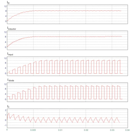

Figure 15. Output waveforms
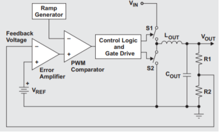
Figure 16. Duty ratio
The buck converter is used to generate a lower output voltage from a higher DC input voltage. If the losses in the switch and catch diode are ignored, then the duty cycle, or the ratio of ON time to the total period, of the converter can be expressed as (1) The duty cycle is determined by the output of the error amplifier and the PWM ramp voltage as shown in Figure 2. The ON time starts on the falling edge of the PWM ramp voltage and stops when the ramp voltage equals the output voltage of the error amplifier. The output of the error amplifier in turn is set so that the feedback portion of the output voltage is equal to the internal reference voltage.

Figure 17. Output of error amplifier
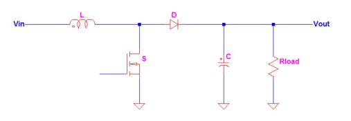
A typical Boost converter is shown below.
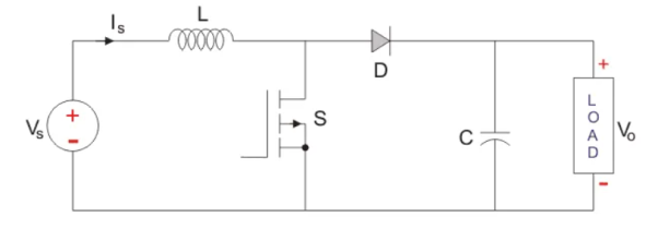
The input voltage source is connected to an inductor. The solid-state device which operates as a switch is connected across the source. The second switch used is a diode. The diode is connected to a capacitor, and the load and the two are connected in parallel as shown in the figure above.
The inductor connected to input source leads to a constant input current, and thus the Boost converter is seen as the constant current input source. And the load can be seen as a constant voltage source.
The controlled switch is turned on and off by using Pulse Width Modulation (PWM). The Boost converter has two modes of operation. The first mode is when the switch is on and conducting.
Mode I: Switch is ON, Diode is OFF
The switch is ON and therefore represents a short circuit ideally offering zero resistance to the flow of current so when the switch is ON all the current will flow through the switch and back to the DC input source. Let us say the switch is on for a time TON and is off for a time TOFF. We define the time period, T, as
T = TON + T OFF
And the switching frequency
Fswitching = 1/T.
Let us now define another term, the duty cycle,
D = TON/T
Let us analyze the Boost converter in steady state operation for this mode using KVL.
Vin = VL
VL = L diL /dt = Vin
DiL/dt = ∆ iL/∆t = ∆iL/DT = Vin/L
Since the switch is closed for a time Ton = DT we can say that ∆t=DT
(∆ iL) closed= (Vin/L) DT
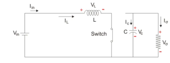
Let us analyze the Boost converter in steady state operation for this mode using KVL. Since the switch is closed for a time TON = DT we can say that Δt = DT.
While performing the analysis of the Boost converter, we have to keep in mind that
The inductor current is continuous and this is made possible by selecting an appropriate value of L.
The inductor current in steady state rises from a value with a positive slope to a maximum value during the ON state and then drops back down to the initial value with a negative slope. Therefore, the net change of the inductor current over anyone complete cycle is zero.
Mode II: Switch is OFF, Diode is ON
In this mode, the polarity of the inductor is reversed. The energy stored in the inductor is released and is ultimately dissipated in the load resistance, and this helps to maintain the flow of current in the same direction through the load and also step-up the output voltage as the inductor is now also acting as a source in conjunction with the input source. But for analysis, we keep the original conventions to analyze the circuit using KVL.
Let us now analyse the Boost converter in steady state operation for Mode II using KVL.
Vin = VL + Vo
VL = L diL/dt = Vin -VO
DiL/dt = ∆ iL/∆t = ∆ iL / (1-D) T = Vm-Vo/L
Since the switch is open for a time
TOFF = T – TON = T -DT = (1-D) T
We can say that
∆t = (1-D) T
(∆ iL) open = (Vin -Vo/L) (1-D) T
It is already established that the net change of the inductor current over any one complete cycle is zero
(∆ iL) closed + (∆ iL) open =0
(Vin – Vo) /L (1-D) T + (-Vo/L) DT =0
Vo /Vin = 1/ 1-D
Since the switch is open for a time
TOFF = T – TON = T – DT = (1-D) T
We can say that
∆t = (1-D) T
It is already established that the net change of the inductor current over any one complete cycle is zero.
(∆ iL) closed + (∆ iL) open =0
(Vin – Vo/L) (1-D) T + (-Vo/L) DT =0
Vo /Vin = 1/ 1-D
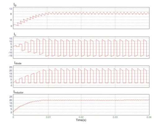
A circuit of a Boost converter and its waveforms are shown below. The inductance, L, is 20mH and the C is 100µF and the resistive load is 20Ω. The switching frequency is 1 kHz. The input voltage is 100V DC and the duty cycle is 0.5.
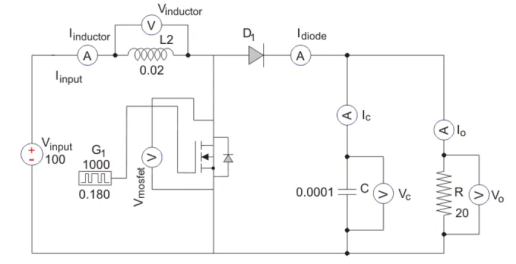
The voltage waveforms are as shown above and the current waveforms are as shown in the figure below.
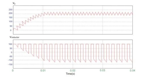
The voltage waveforms are as shown above and the current waveforms are as shown in the figure below.
The inductor of the boost converter charges during Ton and discharges during Toff. The inductor current waveform is then resembled like Figure 2 below.
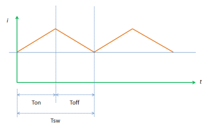
The figure is an inductor waveform of a continuous conduction mode boost converter. A boost converter by the way can operate in three modes; continuous conduction (CCM), discontinuous conduction (DCM) and boundary mode. For CCM the inductor current will not reach zero after every switching cycle. For DCM, the inductor current is reaching zero before the next Ton occur.
How to Calculate the Duty Cycle of Boost Converter – Analysis during Ton
During Ton, the switch S is on. The diode will be reversed biased and this time the load is being supplied by the energy stored in the capacitor C. The inductor will charge. The flow of the current is from Vin to inductor L then to switch S. By KVL,
Vin – VL – Vsw = 0
Then expressing VL
VL = Vin – Vsw …………………..(1)
The voltage across inductor is also defined by below formula.
VL = L di/dt ……………(2)
Expressing the change in current di
Di = VL/L dt ……………………...(3)
Substitute 1 to 3
Di = (Vin – Vsw)/L dt ……………(4)
Then we will get rid of the variable dt by integrating the equation from 0 to Ton.


How to Calculate the Duty Cycle of Boost Converter – Analysis during Toff
During Toff, the inductor reverses its polarity and the diode at this time w ill be forward biased and the load will be supplied by the energy in the inductor. The energy on the inductor will start to decay. The flow of current is from Vin to diode D then to the load. Applying KVL,
Vin + VL – VF - Vout = 0
Expressing VL,
VL = Vout + VF – Vin ………….(6)
Substituting [Eq. 6] to [Eq. 3] will result to

Then we will eliminate the variable dt through integration from Ton to T.


Now go back to Figure 2, the magnitude of the inductor current during Ton and Toff is equal. Therefore, we can equate [Eq. 5] and [Eq. 8].


Ton(Vin – Vsw) = (T – Ton)(Vout + VF – Vin)
Then substitute Ton = DT
DTV in – DTV sw = T(1 – D)(Vout + VF – Vin)
Then solving for the duty cycle, D
D = (Vout + VF – Vin)/(Vout + VF – Vsw ) …………………(9)
Eq. 9
Assuming ideal values (diode and switch voltage drops are zero)
D = (Vout – Vin)/Vout ………….(10)
Output Voltage:
The relationship of voltage and current for an inductor is:
I = 1/L  , or
, or
V = L di/dt
For a constant rectangular pulse:
I = Vt /L + i0
From this we can see that the current is a linear ramp, when the voltage is a constant pulse.
When the transistor switches on the current is:

, or

And when the transistor switches off the current is:
i0 = ipk – (Vout – Vin + VD)Toff/L , or

(Equation 1)
Where VD is the voltage drop across the diode, and VTrans is the voltage drop across the transistor. Note that the continuous/discontinuous boundary occurs when io is zero.
By equating through delta i, we can solve for Vout:

Vin Ton – VTrans Ton = Vout Toff – Vin Toff + VDToff
Vin Ton + VinToff = VoutToff + VTransTon + VDToff
Vin – VTrans D = (Vout + VD)(1 – D)
Vout = (Vin – VTransD)/(1 – D) - VD
We can also solve for the duty cycle as follows,
DVout + DVD – VTrans D = Vout – Vin + VD
D = ( Vout – Vin + VD)/(Vout + VD – VTrans)
If we neglect the voltage drops across the transistor and diode then:
Vout = Vin/(1 – D)
So, it is clear that the output voltage is related directly to the duty cycle of the pulses.
References:
- Fundamentals of Power Electronics Book by Robert Warren Erickson
- Power Electronics: Principles and Applications Book by Joseph Vithayathil
- Introduction to power electronics Book by Denis Fewson
- R. W. Erickson and D. Maksimovic, “Fundamentals of Power Electronics”, Springer Science & Business Media, 2007.
- L. Umanand, “Power Electronics: Essentials and Applications”, Wiley India, 2009.