Unit - 4
8051 Microcontroller
8-bit Microprocessor Architecture
- It is a controlling unit that is fabricated on a small chip.
- It is capable to perform arithmetic logic operations and communicate with various devices connected to it.
- It comprises of an ALU (Arithmetic Logic Unit), MU (Memory unit) and CU (Control unit).
- It also consists of register array with registers named as B, C, D, E, H, L and ACC.
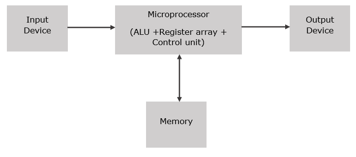
Fig.1: Basic block diagram of microprocessor
Architecture of 8085
- It includes the timing & control unit, Arithmetic and logic unit, decoder, instruction register, interrupt control, a register array, serial input/output control and the central processing unit.

Figure 2. 8085 8-bit Microprocessor architecture
The 8085 microprocessor is an 8-bit processor available as a 40-pin IC package and uses +5 V for power. The data bus width is 8-bit and address bus is 16-bit, therefore it can address 216 = 64 KB of memory.
Arithmetic and Logic Unit:
The ALU performs the arithmetic and logical operations such as Addition (ADD), Subtraction (SUB), AND, OR etc. It uses data from memory and from Accumulator to perform operations. The results of the arithmetic and logical operations are stored in the accumulator.
Registers
The 8085 includes six registers, one accumulator and one flag register, as shown in Figure. In addition, it has two 16-bit registers: stack pointer and program counter.
8085 has six general-purpose registers to store 8-bit data; these are identified as B, C, D, E, H and L. If combined the register pairs - BC, DE and HL perform some 16-bit operations. The programmer can use these registers to store or copy data into the register by using data copy instructions.
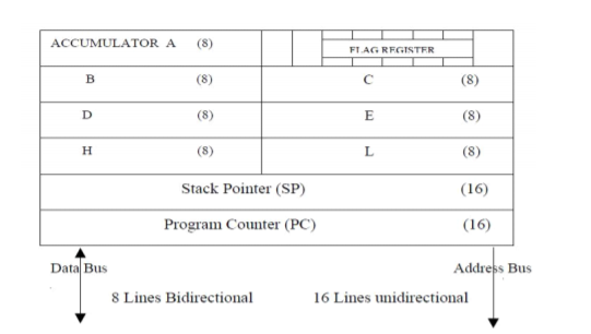
Figure 3. Register Organisation
Program Counter (PC): The 16-bit register deals with sequencing the execution of instructions. This register is a memory pointer. The microprocessor uses this register to sequence the execution of the instructions. The function of the program counter is to point to the memory address from which the next byte is to be fetched. When byte is being fetched, the program counter is automatically incremented by one to point to the next memory location.
Stack Pointer (SP): The stack pointer is also a 16-bit register, used as a memory pointer. It points to a memory location in R/W memory, called stack. The beginning of the stack is defined by loading 16- bit address in the stack pointer.
Instruction Register/Decoder: This is an 8-bit register that temporarily stores the current instruction of a program. Decoder then takes instruction and decodes or interprets the instruction. Decoded instruction then passed to next stage.
Control Unit: Generates signals on data bus, address bus and control bus within microprocessor to carry out the instruction, which has been decoded.
Typical buses and their timing are:
• Data Bus: Data bus carries data in binary form between microprocessor and other external units such as memory. It is used to transmit data that is information, results of arithmetic etc between memory and the microprocessor. Data bus is bidirectional in nature.
• Address Bus: The address bus carries address and is one way bus from microprocessor to the memory or other devices. 8085 microprocessors contain 16-bit address bus and are generally identified as A0 - A15. The higher order address lines (A8 – A15) are unidirectional and the lower order lines (A0 – A7) are multiplexed (time-shared) with the eight data bits (D0 – D7) and hence, they are bidirectional.
• Control Bus: Control bus are various lines which have specific functions for coordinating and controlling microprocessor operations. The control bus carries control signals partly unidirectional and partly bidirectional.
8-bit Microcontroller architecture

Fig:4 8051 Architecture
Central Processor Unit (CPU)
The brain of any processing device of the microcontroller is the CPU. It monitors and controls all operations performed on these units. It reads a program written in ROM memory, executes and does the expected task.
Interrupts
Interrupt is a subroutine call that interrupts the microcontroller's main operations or work and causes it to execute any other program, at the time of operation. It provides a mechanism to put on hold the ongoing operations, execute a subroutine and resume to another type of operation.
8051 has five interrupt sources:
INTO
TFO
INT1
TF1
R1/T1
(INT0) ̅ and (INT1) ̅ are external interrupts negative edge triggered or low level triggered. When these interrupts are activated, the corresponding flags are set except for serial interrupts.
When the processor branches to ISR the interrupt flags are cleared. The external interrupts are timer and serial port interrupts.
Memory
They require memory to save as well as read so that the microcontroller performs specific operations of the task.
The memory which is used to store the program is known as code memory or Program memory. It is also known as ROM memory.
8051 data memory is used to store data temporarily for operation known as RAM memory. It has 4K of code memory or program memory and 128 bytes of data memory of RAM.
BUS
A collection of wires that work as a communication channel or medium for transfer of data. It consists of 8, 16 or more wires of microcontroller. Thus, they carry 8 bits or 16 bits of data simultaneously. There are two types of buses which are
Address Bus
Data Bus
Address Bus:
Microcontroller 8051 has a 16-bit address bus for transferring data. It addresses memory locations to transfer addresses from CPU to Memory. It has four addressing modes that are:
Immediate addressing modes.
Bank address (or) Register addressing mode.
Direct Addressing mode.
Register indirect addressing mode.
Data Bus: Microcontroller 8051 has 8 bits of data bus used to carry data for applications.
Oscillator
The 8051 microcontroller has an on-chip oscillator that acts as a clock source for the CPU of the microcontroller. The output pulses of the oscillator are stable. Therefore, it enables synchronized work for all the parts of the Microcontroller system.
Input/Output Port
To control the operation of machines, microcontrollers are used in embedded systems. To connect to other machines, devices or peripherals I/O interfacing ports is required. Microcontroller 8051 has 4 input and output ports to connect to other peripherals
Timers/Counters
The 8051 microcontroller has two 16-bit timers and counters. The counters are again divided into 8-bit registers. Timers are used for measurement of time intervals to determine pulse width.
Most 8-bit processors are old architectures, so they tend to be slower. They are cheap. They also tend to have a low limit on supported RAM/other storage, but the actual amount depends on the family.
16-bit processors tend to focus on price as well, but there is a large range of parts available, some of which have fairly high performance and large amounts of on-chip peripherals. These parts usually perform faster than 8-bit parts on math where the precision is greater than 8 bits, and tend to have more addressable memory.
32-bit chips compete primarily on performance for an application. There is a considerable range of 32-bit parts available, each targeted at some specific application. They tend to come loaded with peripherals and compete on feature completeness. They have a large amount of addressable memory and the performance tends to be better than 16-bit parts.
An embedded system can be a computer hardware system having software embedded in it. An embedded system can be an independent system or it can be a part of a large system. An embedded system is a microcontroller or microprocessor based system designed to perform a specific task.
For example, let us consider the fire alarm as an embedded system. This system only senses smoke.
An embedded system consists of three components −
It has hardware.
It has application software.
It has a Real Time Operating system (RTOS) which defines the way the system works. It sets the rules during the execution of the application program. A small scale embedded system may not have RTOS.
Characteristics of an Embedded System
Single-functioned − An embedded system usually performs a specialized operation and does the same repeatedly. For example: A pager always functions as a pager.
Tightly constrained − All computing systems have constraints on design metrics, but those on an embedded system can be especially tight. Design metrics is a measure of an implementation's features such as its cost, size, power, and performance
Reactive and Real time − Many embedded systems must continually react to changes in the system's environment and must compute certain results in real time without any delay.
Memory − It must have a memory, as its software usually embeds in ROM. It does not need any secondary memories in the computer.
Connected − It must have connected peripherals to connect input and output devices.
HW-SW systems − Software is used for more features and flexibility. Hardware is used for performance and security.
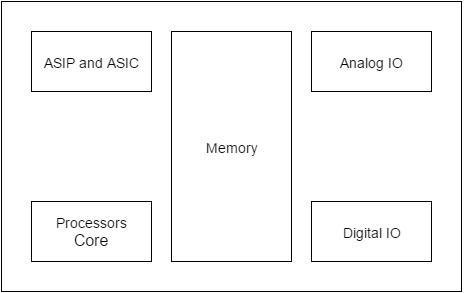
While developing an embedded system there is an option to base the computational hardware around a microcontroller which can be a microcontroller or microprocessor.
Both approaches have their attractions but typically the microcontroller, MCU, is found in applications where size, low power and low cost are key requirements.
The MCU microcontroller is different to a microprocessor where it contains more elements of the overall processing engine within the one chip.
Most of the processing engine components are brought onto a single chip which reduces size and cost. This enables it to become economically viable to digitally control where more devices and processes take place. Also, it is found that mixed signal microcontrollers are being increasingly used, integrating analogue components needed to control non-digital electronic systems.
Microcontrollers comprise the main elements of a small computer system on a single chip. They contain the memory, and IO as well as the CPU one the same chip. This considerably reduces the size, making them ideal for small embedded systems.
Also microcontrollers are often intended for low power and low processing applications where some microcontrollers use 4 bit words and they may also operate with very low clock rates - some 10 kHz and less to conserve power. This means that some MCUs consume a milliwatt or so and they may also have sleep consumption levels of a few nanowatts.
The 8051 Microcontroller is one of the basic type of microcontroller, designed by Intel in 1980’s.
This microcontroller was based on Harvard Architecture and developed primarily for use in embedded systems technology.
Normally, this microcontroller was developed using NMOS technology, which requires more power to operate.
Therefore, Intel redesigned Microcontroller 8051 using CMOS technology and their updated versions came with a letter C for instance an 80C51 which is an 8 bit microcontroller.
These latest Microcontrollers requires less power to operate in comparison to their previous versions.
The 8051 Microcontroller has two buses and two memory spaces of 64K X 8 size for program and data units. It has an 8-- bit processing unit and 8- bit accumulator units.
Architecture of 8051

In the following diagram, the system bus connects all the support devices to the CPU. The system bus consists of an 8-bit data bus, a 16-bit address bus and bus control signals. All other devices like program memory, ports, data memory, serial interface, interrupt control, timers, and the CPU are all interfaced together through the system bus.
Key Takeaways:
It is an 8-bit microcontroller. It is built with 40 pins DIP (dual inline package), 4kb of ROM storage and 128 bytes of RAM storage, 2 16-bit timers.
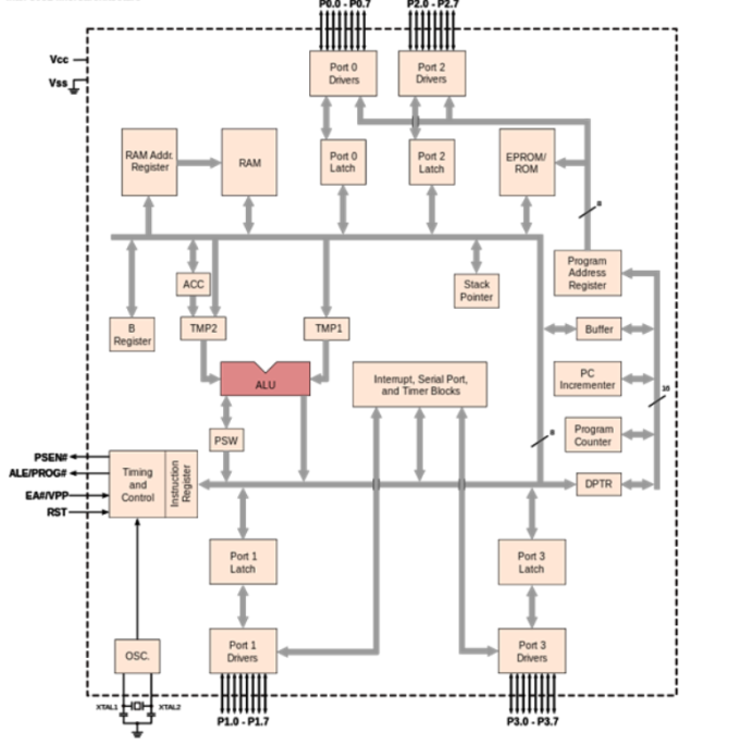
8051 microcontrollers were designed by Intel in 1981. It is an 8-bit microcontroller. It is built with 40 pins DIP (dual inline package), 4kb of ROM storage and 128 bytes of RAM storage, 2 16-bit timers. It consists of four parallel 8-bit ports, which are programmable as well as addressable as per the requirement.
The reasons for the popularity of 8051 Microcontroller are –
Simple to integrate in any electronic device.
Affordable.
Simple architecture.
Easy instruction set.
Low computing power.
The CPU acts as a mind of any processing machine. It synchronizes and manages all processes that are carried out in microcontrollers. The user has no power to control the functioning of the CPU. It interprets the program stored in ROM and carries out from storage and then performs it projected duty. CPUs manage the different types of registers available in 8051 microcontrollers.
It is the heart of the Microcontroller that mainly comprises an Arithmetic Logic Unit (ALU) and a Control Unit (CU) and other important components. The CPU is the primary device in communicating with peripheral devices like Memory, Input and Output.
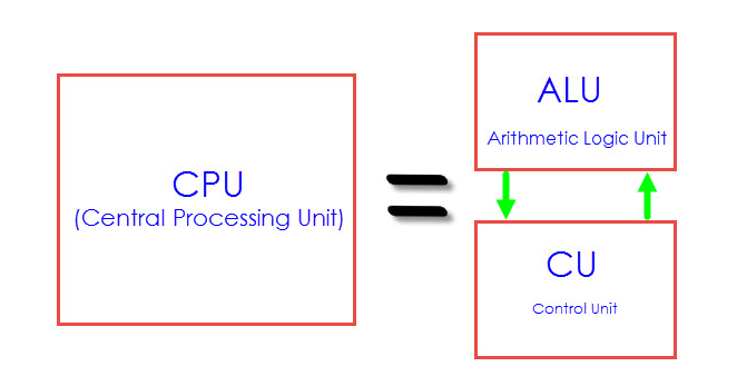
ALU performs all arithmetic and logical functions.
Addition, subtraction with carry, and multiplication are categorized as arithmetic operations.
Logical AND, OR and exclusive OR (XOR) as logical operations.
A bus consists of a group of wires to transfer data from one location to another within the system. Buses reduce the number of paths or cables needed to set up connection between components.
There are two kinds of buses - Data Bus and Address Bus
Data Bus: The purpose of a data bus is to transfer data. It acts as a channel for data to travel.
Address Bus: The purpose of address bus is to transfer information but not data. The information tells from where within the components, the data should be sent to or received from.
Control bus - carries control signals from the processor to other components. The control bus also carries the clock's pulses. The control bus is unidirectional
General Purpose Registers

Figure 5. General Purpose Memory
The general-purpose memory is called as the RAM of the 8051 microcontrollers, which is divided into 3 areas such as banks, bit-addressable area, and scratch-pad area.
The banks contain different general-purpose registers such as R0-R7, and all such registers are byte-addressable registers that store or remove only 1-byte of data.
Banks and Registers
The B0, B1, B2, and B3 stand for banks, and each bank contains eight general-purpose registers ranging from ‘R0’ to ‘R7’. All these registers are byte-addressable. Data transfer between general-purpose registers to general-purpose registers is not possible. These banks are selected by the Program Status Word (PSW) register.

Figure 6. Bank Registers
SFRs related to the I/O ports: The 8051 has four I/O ports of 8 bits, for a total of 32 I/O lines. Whether a given I/O line is high or low and the value read from the line are controlled by the SFRs.
The SFRs control the operation or the configuration of some aspect of the 8051. For example, TCON controls the timers, SCON controls the serial port, the remaining SFRs, are auxiliary which means SFRs don't directly configure 8051. For example, once the serial port has been configured using SCON, the program may read or write to the serial port using the SBUF register.
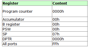
RESET is an active High input. When RESET is set to High, 8051 goes back to the power on state. The 8051 is reset by holding the RST high for at least two machine cycles and then returning it low.
There are two method of reset circuit:
1. Power On Reset.
- Initially charging of capacitor makes RST High
- When capacitor charges fully it blocks DC.
2. Manual Reset
- Closing the switch momentarily will make RST High.

Figure 7. Power and Reset Circuit
After a reset, the program counter is loaded with 0000H but the content of on-chip RAM is not affected.

OSCILLATOR CIRCUIT OF 8051 CONTROLLER
- The 8051 uses the crystal for precisely that to synchronize it’s operation. Effectively, the 8051 operates called as "machine cycles."
- A single machine cycle is the minimum amount of time in which a single 8051 instruction can be executed. Although many instructions take multiple cycles.
- 8051 has an on-chip oscillator. It needs an external crystal that decides the operating frequency of the 8051.

Figure 8. Oscillator circuit
This can be achieved in two ways.
- The crystal is connected to pins 18 and 19 with stabilizing capacitors. 12 MHz (11.059MHz) crystal is often used and the capacitance ranges from 20pF to 40pF.
- The oscillator can also be a TTL clock source connected with a NOT gate as shown.
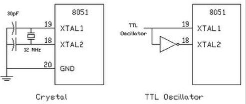
Figure 9. Crystal Oscillator Circuit
Stack:
The stack is a section of RAM used by the CPU to store information temporarily. This information could be data or an address. The CPU needs this storage area since there are only a limited number of registers.
The register used to access the stack is called the SP (stack pointer) register. The stack pointer is 8 bits wide, which takes values of 00 to FFH.
When the 8051 is powered up, the SP register contains value 07. This means that RAM location 08 is the first location used for the stack by the 8051. The storing of a CPU register in the stack is called a PUSH, and pulling the contents off the stack back into a CPU register is called a POP.
Pushing onto the stack
In the 8051 the stack pointer (SP) points to the last used location of the stack. When we push data onto the stack, the stack pointer (SP) is incremented by one.
The SP is decremented when data is pushed onto the stack.
For example, when PUSH is executed, the contents of the register are saved on the stack and SP is incremented by 1.
For example, the instruction “PUSH 1″ pushes register Rl onto the stack.
Show that the stack and stack pointer for the following. Assume the default stack area and register 0 is selected.
MOV R6, #25H
MOV R1,#12H
MOV R4, #0F3H
PUSH 6
PUSH 1
PUSH 4
Solution:
| After PUSH 6 | After PUSH 1 | After PUSH 4 |
0B | 0B | 0B | 0B |
0A | 0A | 0A | 0A F3 |
09 | 09 | 09 12 | 09 12 |
08 | 08 25 | 08 25 | 08 25 |
Start SP=07 SP=08 SP=09 SP=0A
Popping from the stack
Popping the contents of the stack back into a given register is the opposite process of pushing. With every pop, the top byte of the stack is copied to the register specified by the instruction and the stack pointer is decremented once.
Example:
Examine the stack shows the contents of the registers and SP after execution of the following instructions.
POP 3 ; POP stack into R3
POP 5; POP stack into R5
POP 2; POP stack into R2
Solution:
| After PUSH 6 | After PUSH 1 | After PUSH 4 |
0B 54 | 0B | 0B | 0B |
0A F9 | 0A F9 | 0A | 0A |
09 76 | 09 76 | 09 76 | 09 |
08 6C | 08 6C | 08 6C | 08 6C |
Start SP=0B SP=0A SP=09 SP=08
Stack Pointer (SP)
SP or Stack Pointer points to the top of the Stack and it indicates the next data to be accessed. Stack Pointer can be accessed using PUSH, POP, CALL and RET Instructions. The Stack Pointer is an 8-bit register and upon reset, the Stack Pointer is initialized with 07H.
When writing a new data byte into the stack, the SP (Stack Pointer) is automatically incremented by 1 and the new data is written at an address SP+1. When reading data from stack, the data is retrieved from the Address in SP and after that the SP is decremented by 1 (SP-1)
A program counter is a 16-bit register that has no internal address. The program counter fetches the address of the next instruction to be executed from memory. The PC holds the address of next instruction residing in memory. When a command is encountered, it executes that instruction. PC increments and holds the address of the next instruction.
All 8051 microcontrollers have 4 I/O ports each comprising 8 bits which can be configured as inputs or outputs. Accordingly, in total of 32 input/output pins enabling the microcontroller to be connected to peripheral devices are available for use.
To configure a microcontroller pin as an input, it is necessary to apply a logic zero (0) to appropriate I/O port bit.
To configure a microcontroller pin as an input, it is necessary to apply a logic one (1) to appropriate port. In this case, voltage level on appropriate pin will be 5V (as is the case with any TTL input.
Port 0

Figure 10. Input
If any pin of this port is configured as an input then it acts as if it “floats”. Such an input has unlimited input resistance and indetermined potential.
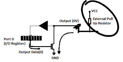
Figure 11. Output
When the pin is configured as an output, it acts as an “open drain”. By applying logic 0 to a port bit, the appropriate pin will be connected to ground (0V). To apply logic 1 (5V) on this output pin, it is necessary to build in an external pull-up resistor.
Port 1
P1 is a true I/O port, because it doesn't have any alternative functions as is the case with P0, but can be configured as general I/O only. It has a pull-up resistor built-in and is completely compatible with TTL circuits.
Port 2
P2 acts similarly to P0 when external memory is used. Pins of this port occupy addresses intended for external memory chip. This time it is about the higher address byte with addresses A8-A15. When no memory is added, this port can be used as a general input/output port showing features similar to P1.
Port 3
All port pins can be used as general I/O, but they also have an alternative function. To use these alternative functions, a logic one (1) must be applied to appropriate bit of the P3 register.
The internal data memory of 8051 is divided into two groups. These are a set of eight registers and a scratch pad memory. These eight registers are R0 toR7. The address range 00H to 07H is used to access the registers, and the rest are scratch pad memory.
8051 Provides four register bank, but only one register bank can be used at any point in time. To select the register bank, two bits of PSW (Program Status Word) are used.
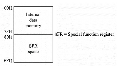
Figure 12. Register Bank
So, the following addressing can be used to select register banks.
The concept of four register banks is very useful. For servicing the interrupts, this feature is good. The interrupt program can use one bank, and the interrupt Service Subroutine (ISS) can access another bank for better performance. As there are four banks, so for nested interrupts these can be used

Figure 13. Register Bank Selection
When all of the register banks are being used, the scratch pad area will be 20H to 7FH. But from 20H to 2FH (16 bytes or 128 bits) can be used as bit addressable RAM. Another section of bit addressable locations is 80H to FFH. The remaining locations (30H to 7EH) of the RAM can be used to store variable data and stack.

Figure 14. Bit Addressable area
The 8051 Microcontroller Memory is separated into Program Memory (ROM) and Data Memory (RAM). The Program Memory of the 8051 Microcontroller is used for storing the program to be executed, which means instructions. The Data Memory is used for storing temporary variable data and intermediate results.
Program Memory (ROM) of 8051
The code or instructions which are to be executed are stored in the Program Memory, also called as the ROM of the Microcontroller.

Figure 15. Program Memory
In 4KB Internal ROM, the address space is 0000H to 0FFFH. If the program addresses exceed this value, CPU will automatically fetch the code from the external Program Memory.
For External Access (EA Pin) must be pulled HIGH at this condition the CPU first fetches instructions from the Internal Program Memory in the address range of 0000H to 0FFFFH. If it exceeds the memory addresses limit, instructions are fetched from external ROM in address range of 1000H to FFFFH.
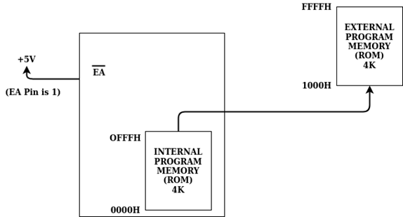
Figure 16. External access
There is also an alternative method to fetch the instructions where the Internal ROM is ignored and instructions are fetched only from External Program Memory (External ROM).
For this purpose, EA pin must be connected to GND. The memory addresses of external ROM will be from 0000H to FFFFH.

Figure 17. External Program Memory
Data Memory (RAM)
Data Memory or RAM stores temporary data and intermediate results generated during the normal operation of the microcontroller.
Currently, 8051 Microcontroller has 256B of RAM. The first 128B memory addresses from 00H to 7FH is divided in to Working Registers. They are organized as Register Banks, Bit – Addressable Area and General-Purpose RAM known as Scratchpad area.
The first 128B of RAM (from 00H to 7FH), the first 32B of memory from addresses 00H to 1FH consists of 32 Working Registers organized into four banks with 8 Registers in each Bank.
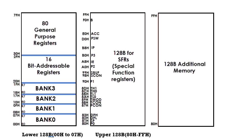
Fig 18. (Direct and Indirect Addressing) (Direct Addressing) (Indirect Addressing)
The 4 banks are named as Bank0, Bank1, Bank2 and Bank3. Each Bank consists of 8 registers R0 – R7. Each Register can be addressed either by name or by address.
To address the register by name, first the corresponding bank is selected. In order to select the bank, RS0 and RS1 bits of the Program Status Word (PSW) and Register (RS0 and RS1 are 3rd and 4th bits in the PSW Register) are used.
When addressing these Register for example 12H the corresponding bank may or may not be selected. (12H corresponds to R2 in Bank2).
The next 16B of the RAM that is from 20H to 2FH are Bit – Addressable memory locations. A total of 128 bits can be addressed individually using 00H to 7FH or an entire byte can be addressed as 20H to 2FH.
The final 80B of the internal RAM addresses are from 30H to 7FH which is the general-purpose RAM area are byte addressable.
These lower 128B of RAM can be addressed directly or indirectly.
Key takeaway
- For External Access (EA Pin) must be pulled HIGH at this condition the CPU first fetches instructions from the Internal Program Memory in the address range of 0000H to 0FFFFH. If it exceeds the memory addresses limit, instructions are fetched from external ROM in address range of 1000H to FFFFH.
- Currently, 8051 Microcontroller has 256B of RAM. The first 128B memory addresses from 00H to 7FH is divided in to Working Registers.
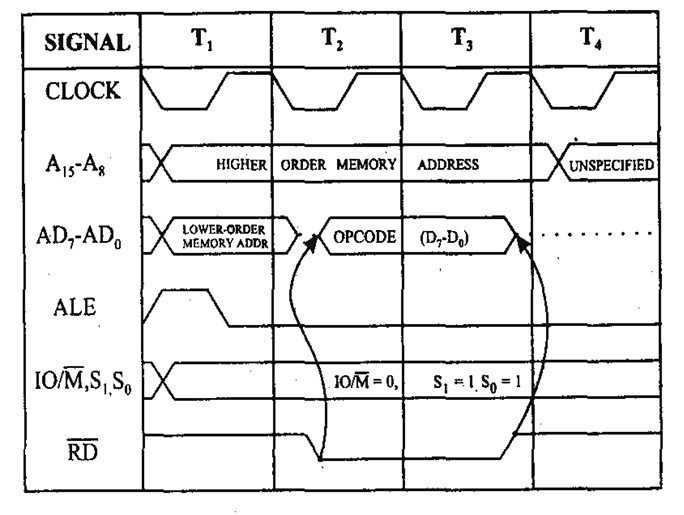
The processor decodes the instruction in the instruction register and generates the necessary control signals to execute the instruction. Based on the instruction further operations such as fetching, writing into memory etc takes place.

Fig 19. Timing diagram for op-code fetch cycle
Memory Read Machine Cycle:
The memory read cycle is executed by the processor to read a data byte from memory.
The machine cycle is exactly same to opcode fetch except:
a) It has three T-states
b) The S0 signal is set to 0.
The timing diagram of this cycle is given in
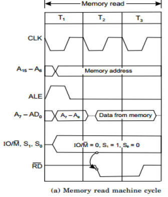
Fig 20. Timing diagram for memory read machine cycle
Memory Write Machine Cycle:
The memory write cycle is executed by the processor to write a data byte in a memory location. The processor takes three T-states and ^(WR) signal is made low. The timing diagram of this cycle is given in Figure.

I/O Read Cycle:
The I/O read cycle is executed by the processor to read a data byte from I/O port or from peripheral, which is I/O mapped in the system. The 8-bit port address is placed both in the lower and higher order address bus. The processor takes three T-states to execute this machine cycle. The timing diagram of this cycle is given in Figure

Fig 21. I/O read machine cycle
References:
- 8051 Microcontroller: An Applications Based Introduction Book by David Calcutt, Frederick J. Cowan, and Hassan Parchizadeh
- 8051 Microcontrollers: Internals, Instructions, Programming, and Interfacing Book by Subrata Ghoshal
- C and the 8051: Building efficient applications Book by Thomas W. Schultz
- MICROCONTROLLER Book by V. Udayashankara
- The 8051/8052 Microcontroller: Architecture, Assembly Language, and Hardware Interfacing Book by Craig Steiner
Unit - 4
8051 Microcontroller
8-bit Microprocessor Architecture
- It is a controlling unit that is fabricated on a small chip.
- It is capable to perform arithmetic logic operations and communicate with various devices connected to it.
- It comprises of an ALU (Arithmetic Logic Unit), MU (Memory unit) and CU (Control unit).
- It also consists of register array with registers named as B, C, D, E, H, L and ACC.

Fig.1: Basic block diagram of microprocessor
Architecture of 8085
- It includes the timing & control unit, Arithmetic and logic unit, decoder, instruction register, interrupt control, a register array, serial input/output control and the central processing unit.
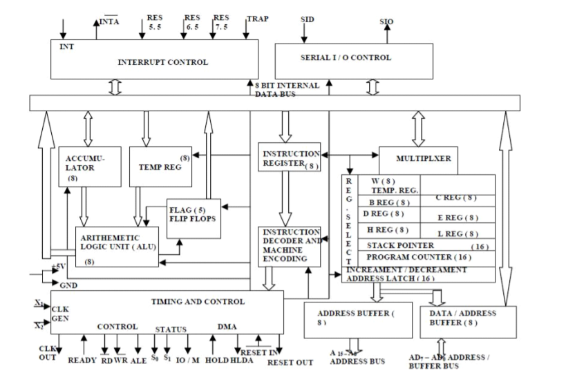
Figure 2. 8085 8-bit Microprocessor architecture
The 8085 microprocessor is an 8-bit processor available as a 40-pin IC package and uses +5 V for power. The data bus width is 8-bit and address bus is 16-bit, therefore it can address 216 = 64 KB of memory.
Arithmetic and Logic Unit:
The ALU performs the arithmetic and logical operations such as Addition (ADD), Subtraction (SUB), AND, OR etc. It uses data from memory and from Accumulator to perform operations. The results of the arithmetic and logical operations are stored in the accumulator.
Registers
The 8085 includes six registers, one accumulator and one flag register, as shown in Figure. In addition, it has two 16-bit registers: stack pointer and program counter.
8085 has six general-purpose registers to store 8-bit data; these are identified as B, C, D, E, H and L. If combined the register pairs - BC, DE and HL perform some 16-bit operations. The programmer can use these registers to store or copy data into the register by using data copy instructions.

Figure 3. Register Organisation
Program Counter (PC): The 16-bit register deals with sequencing the execution of instructions. This register is a memory pointer. The microprocessor uses this register to sequence the execution of the instructions. The function of the program counter is to point to the memory address from which the next byte is to be fetched. When byte is being fetched, the program counter is automatically incremented by one to point to the next memory location.
Stack Pointer (SP): The stack pointer is also a 16-bit register, used as a memory pointer. It points to a memory location in R/W memory, called stack. The beginning of the stack is defined by loading 16- bit address in the stack pointer.
Instruction Register/Decoder: This is an 8-bit register that temporarily stores the current instruction of a program. Decoder then takes instruction and decodes or interprets the instruction. Decoded instruction then passed to next stage.
Control Unit: Generates signals on data bus, address bus and control bus within microprocessor to carry out the instruction, which has been decoded.
Typical buses and their timing are:
• Data Bus: Data bus carries data in binary form between microprocessor and other external units such as memory. It is used to transmit data that is information, results of arithmetic etc between memory and the microprocessor. Data bus is bidirectional in nature.
• Address Bus: The address bus carries address and is one way bus from microprocessor to the memory or other devices. 8085 microprocessors contain 16-bit address bus and are generally identified as A0 - A15. The higher order address lines (A8 – A15) are unidirectional and the lower order lines (A0 – A7) are multiplexed (time-shared) with the eight data bits (D0 – D7) and hence, they are bidirectional.
• Control Bus: Control bus are various lines which have specific functions for coordinating and controlling microprocessor operations. The control bus carries control signals partly unidirectional and partly bidirectional.
8-bit Microcontroller architecture

Fig:4 8051 Architecture
Central Processor Unit (CPU)
The brain of any processing device of the microcontroller is the CPU. It monitors and controls all operations performed on these units. It reads a program written in ROM memory, executes and does the expected task.
Interrupts
Interrupt is a subroutine call that interrupts the microcontroller's main operations or work and causes it to execute any other program, at the time of operation. It provides a mechanism to put on hold the ongoing operations, execute a subroutine and resume to another type of operation.
8051 has five interrupt sources:
INTO
TFO
INT1
TF1
R1/T1
(INT0) ̅ and (INT1) ̅ are external interrupts negative edge triggered or low level triggered. When these interrupts are activated, the corresponding flags are set except for serial interrupts.
When the processor branches to ISR the interrupt flags are cleared. The external interrupts are timer and serial port interrupts.
Memory
They require memory to save as well as read so that the microcontroller performs specific operations of the task.
The memory which is used to store the program is known as code memory or Program memory. It is also known as ROM memory.
8051 data memory is used to store data temporarily for operation known as RAM memory. It has 4K of code memory or program memory and 128 bytes of data memory of RAM.
BUS
A collection of wires that work as a communication channel or medium for transfer of data. It consists of 8, 16 or more wires of microcontroller. Thus, they carry 8 bits or 16 bits of data simultaneously. There are two types of buses which are
Address Bus
Data Bus
Address Bus:
Microcontroller 8051 has a 16-bit address bus for transferring data. It addresses memory locations to transfer addresses from CPU to Memory. It has four addressing modes that are:
Immediate addressing modes.
Bank address (or) Register addressing mode.
Direct Addressing mode.
Register indirect addressing mode.
Data Bus: Microcontroller 8051 has 8 bits of data bus used to carry data for applications.
Oscillator
The 8051 microcontroller has an on-chip oscillator that acts as a clock source for the CPU of the microcontroller. The output pulses of the oscillator are stable. Therefore, it enables synchronized work for all the parts of the Microcontroller system.
Input/Output Port
To control the operation of machines, microcontrollers are used in embedded systems. To connect to other machines, devices or peripherals I/O interfacing ports is required. Microcontroller 8051 has 4 input and output ports to connect to other peripherals
Timers/Counters
The 8051 microcontroller has two 16-bit timers and counters. The counters are again divided into 8-bit registers. Timers are used for measurement of time intervals to determine pulse width.
Most 8-bit processors are old architectures, so they tend to be slower. They are cheap. They also tend to have a low limit on supported RAM/other storage, but the actual amount depends on the family.
16-bit processors tend to focus on price as well, but there is a large range of parts available, some of which have fairly high performance and large amounts of on-chip peripherals. These parts usually perform faster than 8-bit parts on math where the precision is greater than 8 bits, and tend to have more addressable memory.
32-bit chips compete primarily on performance for an application. There is a considerable range of 32-bit parts available, each targeted at some specific application. They tend to come loaded with peripherals and compete on feature completeness. They have a large amount of addressable memory and the performance tends to be better than 16-bit parts.
An embedded system can be a computer hardware system having software embedded in it. An embedded system can be an independent system or it can be a part of a large system. An embedded system is a microcontroller or microprocessor based system designed to perform a specific task.
For example, let us consider the fire alarm as an embedded system. This system only senses smoke.
An embedded system consists of three components −
It has hardware.
It has application software.
It has a Real Time Operating system (RTOS) which defines the way the system works. It sets the rules during the execution of the application program. A small scale embedded system may not have RTOS.
Characteristics of an Embedded System
Single-functioned − An embedded system usually performs a specialized operation and does the same repeatedly. For example: A pager always functions as a pager.
Tightly constrained − All computing systems have constraints on design metrics, but those on an embedded system can be especially tight. Design metrics is a measure of an implementation's features such as its cost, size, power, and performance
Reactive and Real time − Many embedded systems must continually react to changes in the system's environment and must compute certain results in real time without any delay.
Memory − It must have a memory, as its software usually embeds in ROM. It does not need any secondary memories in the computer.
Connected − It must have connected peripherals to connect input and output devices.
HW-SW systems − Software is used for more features and flexibility. Hardware is used for performance and security.

While developing an embedded system there is an option to base the computational hardware around a microcontroller which can be a microcontroller or microprocessor.
Both approaches have their attractions but typically the microcontroller, MCU, is found in applications where size, low power and low cost are key requirements.
The MCU microcontroller is different to a microprocessor where it contains more elements of the overall processing engine within the one chip.
Most of the processing engine components are brought onto a single chip which reduces size and cost. This enables it to become economically viable to digitally control where more devices and processes take place. Also, it is found that mixed signal microcontrollers are being increasingly used, integrating analogue components needed to control non-digital electronic systems.
Microcontrollers comprise the main elements of a small computer system on a single chip. They contain the memory, and IO as well as the CPU one the same chip. This considerably reduces the size, making them ideal for small embedded systems.
Also microcontrollers are often intended for low power and low processing applications where some microcontrollers use 4 bit words and they may also operate with very low clock rates - some 10 kHz and less to conserve power. This means that some MCUs consume a milliwatt or so and they may also have sleep consumption levels of a few nanowatts.
The 8051 Microcontroller is one of the basic type of microcontroller, designed by Intel in 1980’s.
This microcontroller was based on Harvard Architecture and developed primarily for use in embedded systems technology.
Normally, this microcontroller was developed using NMOS technology, which requires more power to operate.
Therefore, Intel redesigned Microcontroller 8051 using CMOS technology and their updated versions came with a letter C for instance an 80C51 which is an 8 bit microcontroller.
These latest Microcontrollers requires less power to operate in comparison to their previous versions.
The 8051 Microcontroller has two buses and two memory spaces of 64K X 8 size for program and data units. It has an 8-- bit processing unit and 8- bit accumulator units.
Architecture of 8051

In the following diagram, the system bus connects all the support devices to the CPU. The system bus consists of an 8-bit data bus, a 16-bit address bus and bus control signals. All other devices like program memory, ports, data memory, serial interface, interrupt control, timers, and the CPU are all interfaced together through the system bus.
Key Takeaways:
It is an 8-bit microcontroller. It is built with 40 pins DIP (dual inline package), 4kb of ROM storage and 128 bytes of RAM storage, 2 16-bit timers.

8051 microcontrollers were designed by Intel in 1981. It is an 8-bit microcontroller. It is built with 40 pins DIP (dual inline package), 4kb of ROM storage and 128 bytes of RAM storage, 2 16-bit timers. It consists of four parallel 8-bit ports, which are programmable as well as addressable as per the requirement.
The reasons for the popularity of 8051 Microcontroller are –
Simple to integrate in any electronic device.
Affordable.
Simple architecture.
Easy instruction set.
Low computing power.
The CPU acts as a mind of any processing machine. It synchronizes and manages all processes that are carried out in microcontrollers. The user has no power to control the functioning of the CPU. It interprets the program stored in ROM and carries out from storage and then performs it projected duty. CPUs manage the different types of registers available in 8051 microcontrollers.
It is the heart of the Microcontroller that mainly comprises an Arithmetic Logic Unit (ALU) and a Control Unit (CU) and other important components. The CPU is the primary device in communicating with peripheral devices like Memory, Input and Output.

ALU performs all arithmetic and logical functions.
Addition, subtraction with carry, and multiplication are categorized as arithmetic operations.
Logical AND, OR and exclusive OR (XOR) as logical operations.
A bus consists of a group of wires to transfer data from one location to another within the system. Buses reduce the number of paths or cables needed to set up connection between components.
There are two kinds of buses - Data Bus and Address Bus
Data Bus: The purpose of a data bus is to transfer data. It acts as a channel for data to travel.
Address Bus: The purpose of address bus is to transfer information but not data. The information tells from where within the components, the data should be sent to or received from.
Control bus - carries control signals from the processor to other components. The control bus also carries the clock's pulses. The control bus is unidirectional
General Purpose Registers
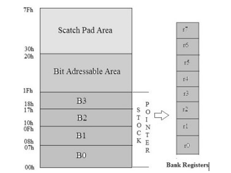
Figure 5. General Purpose Memory
The general-purpose memory is called as the RAM of the 8051 microcontrollers, which is divided into 3 areas such as banks, bit-addressable area, and scratch-pad area.
The banks contain different general-purpose registers such as R0-R7, and all such registers are byte-addressable registers that store or remove only 1-byte of data.
Banks and Registers
The B0, B1, B2, and B3 stand for banks, and each bank contains eight general-purpose registers ranging from ‘R0’ to ‘R7’. All these registers are byte-addressable. Data transfer between general-purpose registers to general-purpose registers is not possible. These banks are selected by the Program Status Word (PSW) register.
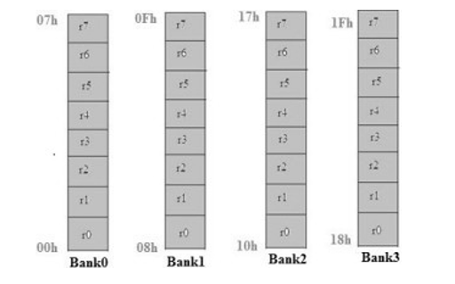
Figure 6. Bank Registers
SFRs related to the I/O ports: The 8051 has four I/O ports of 8 bits, for a total of 32 I/O lines. Whether a given I/O line is high or low and the value read from the line are controlled by the SFRs.
The SFRs control the operation or the configuration of some aspect of the 8051. For example, TCON controls the timers, SCON controls the serial port, the remaining SFRs, are auxiliary which means SFRs don't directly configure 8051. For example, once the serial port has been configured using SCON, the program may read or write to the serial port using the SBUF register.
RESET is an active High input. When RESET is set to High, 8051 goes back to the power on state. The 8051 is reset by holding the RST high for at least two machine cycles and then returning it low.
There are two method of reset circuit:
1. Power On Reset.
- Initially charging of capacitor makes RST High
- When capacitor charges fully it blocks DC.
2. Manual Reset
- Closing the switch momentarily will make RST High.
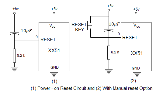
Figure 7. Power and Reset Circuit
After a reset, the program counter is loaded with 0000H but the content of on-chip RAM is not affected.
OSCILLATOR CIRCUIT OF 8051 CONTROLLER
- The 8051 uses the crystal for precisely that to synchronize it’s operation. Effectively, the 8051 operates called as "machine cycles."
- A single machine cycle is the minimum amount of time in which a single 8051 instruction can be executed. Although many instructions take multiple cycles.
- 8051 has an on-chip oscillator. It needs an external crystal that decides the operating frequency of the 8051.

Figure 8. Oscillator circuit
This can be achieved in two ways.
- The crystal is connected to pins 18 and 19 with stabilizing capacitors. 12 MHz (11.059MHz) crystal is often used and the capacitance ranges from 20pF to 40pF.
- The oscillator can also be a TTL clock source connected with a NOT gate as shown.

Figure 9. Crystal Oscillator Circuit
Stack:
The stack is a section of RAM used by the CPU to store information temporarily. This information could be data or an address. The CPU needs this storage area since there are only a limited number of registers.
The register used to access the stack is called the SP (stack pointer) register. The stack pointer is 8 bits wide, which takes values of 00 to FFH.
When the 8051 is powered up, the SP register contains value 07. This means that RAM location 08 is the first location used for the stack by the 8051. The storing of a CPU register in the stack is called a PUSH, and pulling the contents off the stack back into a CPU register is called a POP.
Pushing onto the stack
In the 8051 the stack pointer (SP) points to the last used location of the stack. When we push data onto the stack, the stack pointer (SP) is incremented by one.
The SP is decremented when data is pushed onto the stack.
For example, when PUSH is executed, the contents of the register are saved on the stack and SP is incremented by 1.
For example, the instruction “PUSH 1″ pushes register Rl onto the stack.
Show that the stack and stack pointer for the following. Assume the default stack area and register 0 is selected.
MOV R6, #25H
MOV R1,#12H
MOV R4, #0F3H
PUSH 6
PUSH 1
PUSH 4
Solution:
| After PUSH 6 | After PUSH 1 | After PUSH 4 |
0B | 0B | 0B | 0B |
0A | 0A | 0A | 0A F3 |
09 | 09 | 09 12 | 09 12 |
08 | 08 25 | 08 25 | 08 25 |
Start SP=07 SP=08 SP=09 SP=0A
Popping from the stack
Popping the contents of the stack back into a given register is the opposite process of pushing. With every pop, the top byte of the stack is copied to the register specified by the instruction and the stack pointer is decremented once.
Example:
Examine the stack shows the contents of the registers and SP after execution of the following instructions.
POP 3 ; POP stack into R3
POP 5; POP stack into R5
POP 2; POP stack into R2
Solution:
| After PUSH 6 | After PUSH 1 | After PUSH 4 |
0B 54 | 0B | 0B | 0B |
0A F9 | 0A F9 | 0A | 0A |
09 76 | 09 76 | 09 76 | 09 |
08 6C | 08 6C | 08 6C | 08 6C |
Start SP=0B SP=0A SP=09 SP=08
Stack Pointer (SP)
SP or Stack Pointer points to the top of the Stack and it indicates the next data to be accessed. Stack Pointer can be accessed using PUSH, POP, CALL and RET Instructions. The Stack Pointer is an 8-bit register and upon reset, the Stack Pointer is initialized with 07H.
When writing a new data byte into the stack, the SP (Stack Pointer) is automatically incremented by 1 and the new data is written at an address SP+1. When reading data from stack, the data is retrieved from the Address in SP and after that the SP is decremented by 1 (SP-1)
A program counter is a 16-bit register that has no internal address. The program counter fetches the address of the next instruction to be executed from memory. The PC holds the address of next instruction residing in memory. When a command is encountered, it executes that instruction. PC increments and holds the address of the next instruction.
All 8051 microcontrollers have 4 I/O ports each comprising 8 bits which can be configured as inputs or outputs. Accordingly, in total of 32 input/output pins enabling the microcontroller to be connected to peripheral devices are available for use.
To configure a microcontroller pin as an input, it is necessary to apply a logic zero (0) to appropriate I/O port bit.
To configure a microcontroller pin as an input, it is necessary to apply a logic one (1) to appropriate port. In this case, voltage level on appropriate pin will be 5V (as is the case with any TTL input.
Port 0

Figure 10. Input
If any pin of this port is configured as an input then it acts as if it “floats”. Such an input has unlimited input resistance and indetermined potential.

Figure 11. Output
When the pin is configured as an output, it acts as an “open drain”. By applying logic 0 to a port bit, the appropriate pin will be connected to ground (0V). To apply logic 1 (5V) on this output pin, it is necessary to build in an external pull-up resistor.
Port 1
P1 is a true I/O port, because it doesn't have any alternative functions as is the case with P0, but can be configured as general I/O only. It has a pull-up resistor built-in and is completely compatible with TTL circuits.
Port 2
P2 acts similarly to P0 when external memory is used. Pins of this port occupy addresses intended for external memory chip. This time it is about the higher address byte with addresses A8-A15. When no memory is added, this port can be used as a general input/output port showing features similar to P1.
Port 3
All port pins can be used as general I/O, but they also have an alternative function. To use these alternative functions, a logic one (1) must be applied to appropriate bit of the P3 register.
The internal data memory of 8051 is divided into two groups. These are a set of eight registers and a scratch pad memory. These eight registers are R0 toR7. The address range 00H to 07H is used to access the registers, and the rest are scratch pad memory.
8051 Provides four register bank, but only one register bank can be used at any point in time. To select the register bank, two bits of PSW (Program Status Word) are used.

Figure 12. Register Bank
So, the following addressing can be used to select register banks.
The concept of four register banks is very useful. For servicing the interrupts, this feature is good. The interrupt program can use one bank, and the interrupt Service Subroutine (ISS) can access another bank for better performance. As there are four banks, so for nested interrupts these can be used

Figure 13. Register Bank Selection
When all of the register banks are being used, the scratch pad area will be 20H to 7FH. But from 20H to 2FH (16 bytes or 128 bits) can be used as bit addressable RAM. Another section of bit addressable locations is 80H to FFH. The remaining locations (30H to 7EH) of the RAM can be used to store variable data and stack.
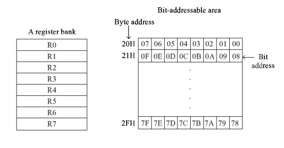
Figure 14. Bit Addressable area
The 8051 Microcontroller Memory is separated into Program Memory (ROM) and Data Memory (RAM). The Program Memory of the 8051 Microcontroller is used for storing the program to be executed, which means instructions. The Data Memory is used for storing temporary variable data and intermediate results.
Program Memory (ROM) of 8051
The code or instructions which are to be executed are stored in the Program Memory, also called as the ROM of the Microcontroller.
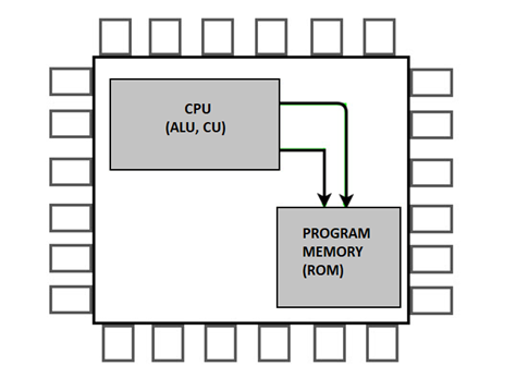
Figure 15. Program Memory
In 4KB Internal ROM, the address space is 0000H to 0FFFH. If the program addresses exceed this value, CPU will automatically fetch the code from the external Program Memory.
For External Access (EA Pin) must be pulled HIGH at this condition the CPU first fetches instructions from the Internal Program Memory in the address range of 0000H to 0FFFFH. If it exceeds the memory addresses limit, instructions are fetched from external ROM in address range of 1000H to FFFFH.

Figure 16. External access
There is also an alternative method to fetch the instructions where the Internal ROM is ignored and instructions are fetched only from External Program Memory (External ROM).
For this purpose, EA pin must be connected to GND. The memory addresses of external ROM will be from 0000H to FFFFH.
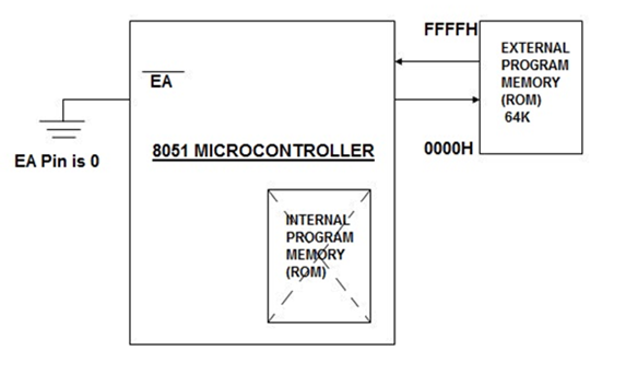
Figure 17. External Program Memory
Data Memory (RAM)
Data Memory or RAM stores temporary data and intermediate results generated during the normal operation of the microcontroller.
Currently, 8051 Microcontroller has 256B of RAM. The first 128B memory addresses from 00H to 7FH is divided in to Working Registers. They are organized as Register Banks, Bit – Addressable Area and General-Purpose RAM known as Scratchpad area.
The first 128B of RAM (from 00H to 7FH), the first 32B of memory from addresses 00H to 1FH consists of 32 Working Registers organized into four banks with 8 Registers in each Bank.

Fig 18. (Direct and Indirect Addressing) (Direct Addressing) (Indirect Addressing)
The 4 banks are named as Bank0, Bank1, Bank2 and Bank3. Each Bank consists of 8 registers R0 – R7. Each Register can be addressed either by name or by address.
To address the register by name, first the corresponding bank is selected. In order to select the bank, RS0 and RS1 bits of the Program Status Word (PSW) and Register (RS0 and RS1 are 3rd and 4th bits in the PSW Register) are used.
When addressing these Register for example 12H the corresponding bank may or may not be selected. (12H corresponds to R2 in Bank2).
The next 16B of the RAM that is from 20H to 2FH are Bit – Addressable memory locations. A total of 128 bits can be addressed individually using 00H to 7FH or an entire byte can be addressed as 20H to 2FH.
The final 80B of the internal RAM addresses are from 30H to 7FH which is the general-purpose RAM area are byte addressable.
These lower 128B of RAM can be addressed directly or indirectly.
Key takeaway
- For External Access (EA Pin) must be pulled HIGH at this condition the CPU first fetches instructions from the Internal Program Memory in the address range of 0000H to 0FFFFH. If it exceeds the memory addresses limit, instructions are fetched from external ROM in address range of 1000H to FFFFH.
- Currently, 8051 Microcontroller has 256B of RAM. The first 128B memory addresses from 00H to 7FH is divided in to Working Registers.
The processor decodes the instruction in the instruction register and generates the necessary control signals to execute the instruction. Based on the instruction further operations such as fetching, writing into memory etc takes place.

Fig 19. Timing diagram for op-code fetch cycle
Memory Read Machine Cycle:
The memory read cycle is executed by the processor to read a data byte from memory.
The machine cycle is exactly same to opcode fetch except:
a) It has three T-states
b) The S0 signal is set to 0.
The timing diagram of this cycle is given in

Fig 20. Timing diagram for memory read machine cycle
Memory Write Machine Cycle:
The memory write cycle is executed by the processor to write a data byte in a memory location. The processor takes three T-states and ^(WR) signal is made low. The timing diagram of this cycle is given in Figure.


I/O Read Cycle:
The I/O read cycle is executed by the processor to read a data byte from I/O port or from peripheral, which is I/O mapped in the system. The 8-bit port address is placed both in the lower and higher order address bus. The processor takes three T-states to execute this machine cycle. The timing diagram of this cycle is given in Figure

Fig 21. I/O read machine cycle
References:
- 8051 Microcontroller: An Applications Based Introduction Book by David Calcutt, Frederick J. Cowan, and Hassan Parchizadeh
- 8051 Microcontrollers: Internals, Instructions, Programming, and Interfacing Book by Subrata Ghoshal
- C and the 8051: Building efficient applications Book by Thomas W. Schultz
- MICROCONTROLLER Book by V. Udayashankara
- The 8051/8052 Microcontroller: Architecture, Assembly Language, and Hardware Interfacing Book by Craig Steiner
Unit - 4
8051 Microcontroller
8-bit Microprocessor Architecture
- It is a controlling unit that is fabricated on a small chip.
- It is capable to perform arithmetic logic operations and communicate with various devices connected to it.
- It comprises of an ALU (Arithmetic Logic Unit), MU (Memory unit) and CU (Control unit).
- It also consists of register array with registers named as B, C, D, E, H, L and ACC.

Fig.1: Basic block diagram of microprocessor
Architecture of 8085
- It includes the timing & control unit, Arithmetic and logic unit, decoder, instruction register, interrupt control, a register array, serial input/output control and the central processing unit.

Figure 2. 8085 8-bit Microprocessor architecture
The 8085 microprocessor is an 8-bit processor available as a 40-pin IC package and uses +5 V for power. The data bus width is 8-bit and address bus is 16-bit, therefore it can address 216 = 64 KB of memory.
Arithmetic and Logic Unit:
The ALU performs the arithmetic and logical operations such as Addition (ADD), Subtraction (SUB), AND, OR etc. It uses data from memory and from Accumulator to perform operations. The results of the arithmetic and logical operations are stored in the accumulator.
Registers
The 8085 includes six registers, one accumulator and one flag register, as shown in Figure. In addition, it has two 16-bit registers: stack pointer and program counter.
8085 has six general-purpose registers to store 8-bit data; these are identified as B, C, D, E, H and L. If combined the register pairs - BC, DE and HL perform some 16-bit operations. The programmer can use these registers to store or copy data into the register by using data copy instructions.

Figure 3. Register Organisation
Program Counter (PC): The 16-bit register deals with sequencing the execution of instructions. This register is a memory pointer. The microprocessor uses this register to sequence the execution of the instructions. The function of the program counter is to point to the memory address from which the next byte is to be fetched. When byte is being fetched, the program counter is automatically incremented by one to point to the next memory location.
Stack Pointer (SP): The stack pointer is also a 16-bit register, used as a memory pointer. It points to a memory location in R/W memory, called stack. The beginning of the stack is defined by loading 16- bit address in the stack pointer.
Instruction Register/Decoder: This is an 8-bit register that temporarily stores the current instruction of a program. Decoder then takes instruction and decodes or interprets the instruction. Decoded instruction then passed to next stage.
Control Unit: Generates signals on data bus, address bus and control bus within microprocessor to carry out the instruction, which has been decoded.
Typical buses and their timing are:
• Data Bus: Data bus carries data in binary form between microprocessor and other external units such as memory. It is used to transmit data that is information, results of arithmetic etc between memory and the microprocessor. Data bus is bidirectional in nature.
• Address Bus: The address bus carries address and is one way bus from microprocessor to the memory or other devices. 8085 microprocessors contain 16-bit address bus and are generally identified as A0 - A15. The higher order address lines (A8 – A15) are unidirectional and the lower order lines (A0 – A7) are multiplexed (time-shared) with the eight data bits (D0 – D7) and hence, they are bidirectional.
• Control Bus: Control bus are various lines which have specific functions for coordinating and controlling microprocessor operations. The control bus carries control signals partly unidirectional and partly bidirectional.
8-bit Microcontroller architecture
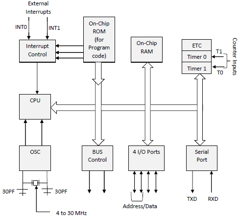
Fig:4 8051 Architecture
Central Processor Unit (CPU)
The brain of any processing device of the microcontroller is the CPU. It monitors and controls all operations performed on these units. It reads a program written in ROM memory, executes and does the expected task.
Interrupts
Interrupt is a subroutine call that interrupts the microcontroller's main operations or work and causes it to execute any other program, at the time of operation. It provides a mechanism to put on hold the ongoing operations, execute a subroutine and resume to another type of operation.
8051 has five interrupt sources:
INTO
TFO
INT1
TF1
R1/T1
(INT0) ̅ and (INT1) ̅ are external interrupts negative edge triggered or low level triggered. When these interrupts are activated, the corresponding flags are set except for serial interrupts.
When the processor branches to ISR the interrupt flags are cleared. The external interrupts are timer and serial port interrupts.
Memory
They require memory to save as well as read so that the microcontroller performs specific operations of the task.
The memory which is used to store the program is known as code memory or Program memory. It is also known as ROM memory.
8051 data memory is used to store data temporarily for operation known as RAM memory. It has 4K of code memory or program memory and 128 bytes of data memory of RAM.
BUS
A collection of wires that work as a communication channel or medium for transfer of data. It consists of 8, 16 or more wires of microcontroller. Thus, they carry 8 bits or 16 bits of data simultaneously. There are two types of buses which are
Address Bus
Data Bus
Address Bus:
Microcontroller 8051 has a 16-bit address bus for transferring data. It addresses memory locations to transfer addresses from CPU to Memory. It has four addressing modes that are:
Immediate addressing modes.
Bank address (or) Register addressing mode.
Direct Addressing mode.
Register indirect addressing mode.
Data Bus: Microcontroller 8051 has 8 bits of data bus used to carry data for applications.
Oscillator
The 8051 microcontroller has an on-chip oscillator that acts as a clock source for the CPU of the microcontroller. The output pulses of the oscillator are stable. Therefore, it enables synchronized work for all the parts of the Microcontroller system.
Input/Output Port
To control the operation of machines, microcontrollers are used in embedded systems. To connect to other machines, devices or peripherals I/O interfacing ports is required. Microcontroller 8051 has 4 input and output ports to connect to other peripherals
Timers/Counters
The 8051 microcontroller has two 16-bit timers and counters. The counters are again divided into 8-bit registers. Timers are used for measurement of time intervals to determine pulse width.
Most 8-bit processors are old architectures, so they tend to be slower. They are cheap. They also tend to have a low limit on supported RAM/other storage, but the actual amount depends on the family.
16-bit processors tend to focus on price as well, but there is a large range of parts available, some of which have fairly high performance and large amounts of on-chip peripherals. These parts usually perform faster than 8-bit parts on math where the precision is greater than 8 bits, and tend to have more addressable memory.
32-bit chips compete primarily on performance for an application. There is a considerable range of 32-bit parts available, each targeted at some specific application. They tend to come loaded with peripherals and compete on feature completeness. They have a large amount of addressable memory and the performance tends to be better than 16-bit parts.
An embedded system can be a computer hardware system having software embedded in it. An embedded system can be an independent system or it can be a part of a large system. An embedded system is a microcontroller or microprocessor based system designed to perform a specific task.
For example, let us consider the fire alarm as an embedded system. This system only senses smoke.
An embedded system consists of three components −
It has hardware.
It has application software.
It has a Real Time Operating system (RTOS) which defines the way the system works. It sets the rules during the execution of the application program. A small scale embedded system may not have RTOS.
Characteristics of an Embedded System
Single-functioned − An embedded system usually performs a specialized operation and does the same repeatedly. For example: A pager always functions as a pager.
Tightly constrained − All computing systems have constraints on design metrics, but those on an embedded system can be especially tight. Design metrics is a measure of an implementation's features such as its cost, size, power, and performance
Reactive and Real time − Many embedded systems must continually react to changes in the system's environment and must compute certain results in real time without any delay.
Memory − It must have a memory, as its software usually embeds in ROM. It does not need any secondary memories in the computer.
Connected − It must have connected peripherals to connect input and output devices.
HW-SW systems − Software is used for more features and flexibility. Hardware is used for performance and security.

While developing an embedded system there is an option to base the computational hardware around a microcontroller which can be a microcontroller or microprocessor.
Both approaches have their attractions but typically the microcontroller, MCU, is found in applications where size, low power and low cost are key requirements.
The MCU microcontroller is different to a microprocessor where it contains more elements of the overall processing engine within the one chip.
Most of the processing engine components are brought onto a single chip which reduces size and cost. This enables it to become economically viable to digitally control where more devices and processes take place. Also, it is found that mixed signal microcontrollers are being increasingly used, integrating analogue components needed to control non-digital electronic systems.
Microcontrollers comprise the main elements of a small computer system on a single chip. They contain the memory, and IO as well as the CPU one the same chip. This considerably reduces the size, making them ideal for small embedded systems.
Also microcontrollers are often intended for low power and low processing applications where some microcontrollers use 4 bit words and they may also operate with very low clock rates - some 10 kHz and less to conserve power. This means that some MCUs consume a milliwatt or so and they may also have sleep consumption levels of a few nanowatts.
The 8051 Microcontroller is one of the basic type of microcontroller, designed by Intel in 1980’s.
This microcontroller was based on Harvard Architecture and developed primarily for use in embedded systems technology.
Normally, this microcontroller was developed using NMOS technology, which requires more power to operate.
Therefore, Intel redesigned Microcontroller 8051 using CMOS technology and their updated versions came with a letter C for instance an 80C51 which is an 8 bit microcontroller.
These latest Microcontrollers requires less power to operate in comparison to their previous versions.
The 8051 Microcontroller has two buses and two memory spaces of 64K X 8 size for program and data units. It has an 8-- bit processing unit and 8- bit accumulator units.
Architecture of 8051

In the following diagram, the system bus connects all the support devices to the CPU. The system bus consists of an 8-bit data bus, a 16-bit address bus and bus control signals. All other devices like program memory, ports, data memory, serial interface, interrupt control, timers, and the CPU are all interfaced together through the system bus.
Key Takeaways:
It is an 8-bit microcontroller. It is built with 40 pins DIP (dual inline package), 4kb of ROM storage and 128 bytes of RAM storage, 2 16-bit timers.

8051 microcontrollers were designed by Intel in 1981. It is an 8-bit microcontroller. It is built with 40 pins DIP (dual inline package), 4kb of ROM storage and 128 bytes of RAM storage, 2 16-bit timers. It consists of four parallel 8-bit ports, which are programmable as well as addressable as per the requirement.
The reasons for the popularity of 8051 Microcontroller are –
Simple to integrate in any electronic device.
Affordable.
Simple architecture.
Easy instruction set.
Low computing power.
The CPU acts as a mind of any processing machine. It synchronizes and manages all processes that are carried out in microcontrollers. The user has no power to control the functioning of the CPU. It interprets the program stored in ROM and carries out from storage and then performs it projected duty. CPUs manage the different types of registers available in 8051 microcontrollers.
It is the heart of the Microcontroller that mainly comprises an Arithmetic Logic Unit (ALU) and a Control Unit (CU) and other important components. The CPU is the primary device in communicating with peripheral devices like Memory, Input and Output.

ALU performs all arithmetic and logical functions.
Addition, subtraction with carry, and multiplication are categorized as arithmetic operations.
Logical AND, OR and exclusive OR (XOR) as logical operations.
A bus consists of a group of wires to transfer data from one location to another within the system. Buses reduce the number of paths or cables needed to set up connection between components.
There are two kinds of buses - Data Bus and Address Bus
Data Bus: The purpose of a data bus is to transfer data. It acts as a channel for data to travel.
Address Bus: The purpose of address bus is to transfer information but not data. The information tells from where within the components, the data should be sent to or received from.
Control bus - carries control signals from the processor to other components. The control bus also carries the clock's pulses. The control bus is unidirectional
General Purpose Registers

Figure 5. General Purpose Memory
The general-purpose memory is called as the RAM of the 8051 microcontrollers, which is divided into 3 areas such as banks, bit-addressable area, and scratch-pad area.
The banks contain different general-purpose registers such as R0-R7, and all such registers are byte-addressable registers that store or remove only 1-byte of data.
Banks and Registers
The B0, B1, B2, and B3 stand for banks, and each bank contains eight general-purpose registers ranging from ‘R0’ to ‘R7’. All these registers are byte-addressable. Data transfer between general-purpose registers to general-purpose registers is not possible. These banks are selected by the Program Status Word (PSW) register.

Figure 6. Bank Registers
SFRs related to the I/O ports: The 8051 has four I/O ports of 8 bits, for a total of 32 I/O lines. Whether a given I/O line is high or low and the value read from the line are controlled by the SFRs.
The SFRs control the operation or the configuration of some aspect of the 8051. For example, TCON controls the timers, SCON controls the serial port, the remaining SFRs, are auxiliary which means SFRs don't directly configure 8051. For example, once the serial port has been configured using SCON, the program may read or write to the serial port using the SBUF register.
RESET is an active High input. When RESET is set to High, 8051 goes back to the power on state. The 8051 is reset by holding the RST high for at least two machine cycles and then returning it low.
There are two method of reset circuit:
1. Power On Reset.
- Initially charging of capacitor makes RST High
- When capacitor charges fully it blocks DC.
2. Manual Reset
- Closing the switch momentarily will make RST High.

Figure 7. Power and Reset Circuit
After a reset, the program counter is loaded with 0000H but the content of on-chip RAM is not affected.

OSCILLATOR CIRCUIT OF 8051 CONTROLLER
- The 8051 uses the crystal for precisely that to synchronize it’s operation. Effectively, the 8051 operates called as "machine cycles."
- A single machine cycle is the minimum amount of time in which a single 8051 instruction can be executed. Although many instructions take multiple cycles.
- 8051 has an on-chip oscillator. It needs an external crystal that decides the operating frequency of the 8051.
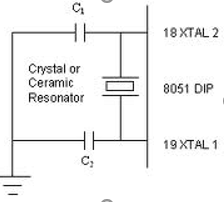
Figure 8. Oscillator circuit
This can be achieved in two ways.
- The crystal is connected to pins 18 and 19 with stabilizing capacitors. 12 MHz (11.059MHz) crystal is often used and the capacitance ranges from 20pF to 40pF.
- The oscillator can also be a TTL clock source connected with a NOT gate as shown.

Figure 9. Crystal Oscillator Circuit
Stack:
The stack is a section of RAM used by the CPU to store information temporarily. This information could be data or an address. The CPU needs this storage area since there are only a limited number of registers.
The register used to access the stack is called the SP (stack pointer) register. The stack pointer is 8 bits wide, which takes values of 00 to FFH.
When the 8051 is powered up, the SP register contains value 07. This means that RAM location 08 is the first location used for the stack by the 8051. The storing of a CPU register in the stack is called a PUSH, and pulling the contents off the stack back into a CPU register is called a POP.
Pushing onto the stack
In the 8051 the stack pointer (SP) points to the last used location of the stack. When we push data onto the stack, the stack pointer (SP) is incremented by one.
The SP is decremented when data is pushed onto the stack.
For example, when PUSH is executed, the contents of the register are saved on the stack and SP is incremented by 1.
For example, the instruction “PUSH 1″ pushes register Rl onto the stack.
Show that the stack and stack pointer for the following. Assume the default stack area and register 0 is selected.
MOV R6, #25H
MOV R1,#12H
MOV R4, #0F3H
PUSH 6
PUSH 1
PUSH 4
Solution:
| After PUSH 6 | After PUSH 1 | After PUSH 4 |
0B | 0B | 0B | 0B |
0A | 0A | 0A | 0A F3 |
09 | 09 | 09 12 | 09 12 |
08 | 08 25 | 08 25 | 08 25 |
Start SP=07 SP=08 SP=09 SP=0A
Popping from the stack
Popping the contents of the stack back into a given register is the opposite process of pushing. With every pop, the top byte of the stack is copied to the register specified by the instruction and the stack pointer is decremented once.
Example:
Examine the stack shows the contents of the registers and SP after execution of the following instructions.
POP 3 ; POP stack into R3
POP 5; POP stack into R5
POP 2; POP stack into R2
Solution:
| After PUSH 6 | After PUSH 1 | After PUSH 4 |
0B 54 | 0B | 0B | 0B |
0A F9 | 0A F9 | 0A | 0A |
09 76 | 09 76 | 09 76 | 09 |
08 6C | 08 6C | 08 6C | 08 6C |
Start SP=0B SP=0A SP=09 SP=08
Stack Pointer (SP)
SP or Stack Pointer points to the top of the Stack and it indicates the next data to be accessed. Stack Pointer can be accessed using PUSH, POP, CALL and RET Instructions. The Stack Pointer is an 8-bit register and upon reset, the Stack Pointer is initialized with 07H.
When writing a new data byte into the stack, the SP (Stack Pointer) is automatically incremented by 1 and the new data is written at an address SP+1. When reading data from stack, the data is retrieved from the Address in SP and after that the SP is decremented by 1 (SP-1)
A program counter is a 16-bit register that has no internal address. The program counter fetches the address of the next instruction to be executed from memory. The PC holds the address of next instruction residing in memory. When a command is encountered, it executes that instruction. PC increments and holds the address of the next instruction.
All 8051 microcontrollers have 4 I/O ports each comprising 8 bits which can be configured as inputs or outputs. Accordingly, in total of 32 input/output pins enabling the microcontroller to be connected to peripheral devices are available for use.
To configure a microcontroller pin as an input, it is necessary to apply a logic zero (0) to appropriate I/O port bit.
To configure a microcontroller pin as an input, it is necessary to apply a logic one (1) to appropriate port. In this case, voltage level on appropriate pin will be 5V (as is the case with any TTL input.
Port 0
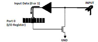
Figure 10. Input
If any pin of this port is configured as an input then it acts as if it “floats”. Such an input has unlimited input resistance and indetermined potential.

Figure 11. Output
When the pin is configured as an output, it acts as an “open drain”. By applying logic 0 to a port bit, the appropriate pin will be connected to ground (0V). To apply logic 1 (5V) on this output pin, it is necessary to build in an external pull-up resistor.
Port 1
P1 is a true I/O port, because it doesn't have any alternative functions as is the case with P0, but can be configured as general I/O only. It has a pull-up resistor built-in and is completely compatible with TTL circuits.
Port 2
P2 acts similarly to P0 when external memory is used. Pins of this port occupy addresses intended for external memory chip. This time it is about the higher address byte with addresses A8-A15. When no memory is added, this port can be used as a general input/output port showing features similar to P1.
Port 3
All port pins can be used as general I/O, but they also have an alternative function. To use these alternative functions, a logic one (1) must be applied to appropriate bit of the P3 register.
The internal data memory of 8051 is divided into two groups. These are a set of eight registers and a scratch pad memory. These eight registers are R0 toR7. The address range 00H to 07H is used to access the registers, and the rest are scratch pad memory.
8051 Provides four register bank, but only one register bank can be used at any point in time. To select the register bank, two bits of PSW (Program Status Word) are used.

Figure 12. Register Bank
So, the following addressing can be used to select register banks.
The concept of four register banks is very useful. For servicing the interrupts, this feature is good. The interrupt program can use one bank, and the interrupt Service Subroutine (ISS) can access another bank for better performance. As there are four banks, so for nested interrupts these can be used
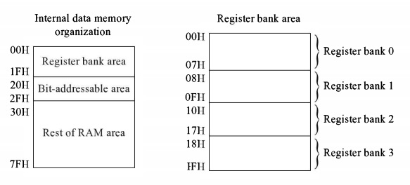
Figure 13. Register Bank Selection
When all of the register banks are being used, the scratch pad area will be 20H to 7FH. But from 20H to 2FH (16 bytes or 128 bits) can be used as bit addressable RAM. Another section of bit addressable locations is 80H to FFH. The remaining locations (30H to 7EH) of the RAM can be used to store variable data and stack.

Figure 14. Bit Addressable area
The 8051 Microcontroller Memory is separated into Program Memory (ROM) and Data Memory (RAM). The Program Memory of the 8051 Microcontroller is used for storing the program to be executed, which means instructions. The Data Memory is used for storing temporary variable data and intermediate results.
Program Memory (ROM) of 8051
The code or instructions which are to be executed are stored in the Program Memory, also called as the ROM of the Microcontroller.

Figure 15. Program Memory
In 4KB Internal ROM, the address space is 0000H to 0FFFH. If the program addresses exceed this value, CPU will automatically fetch the code from the external Program Memory.
For External Access (EA Pin) must be pulled HIGH at this condition the CPU first fetches instructions from the Internal Program Memory in the address range of 0000H to 0FFFFH. If it exceeds the memory addresses limit, instructions are fetched from external ROM in address range of 1000H to FFFFH.

Figure 16. External access
There is also an alternative method to fetch the instructions where the Internal ROM is ignored and instructions are fetched only from External Program Memory (External ROM).
For this purpose, EA pin must be connected to GND. The memory addresses of external ROM will be from 0000H to FFFFH.

Figure 17. External Program Memory
Data Memory (RAM)
Data Memory or RAM stores temporary data and intermediate results generated during the normal operation of the microcontroller.
Currently, 8051 Microcontroller has 256B of RAM. The first 128B memory addresses from 00H to 7FH is divided in to Working Registers. They are organized as Register Banks, Bit – Addressable Area and General-Purpose RAM known as Scratchpad area.
The first 128B of RAM (from 00H to 7FH), the first 32B of memory from addresses 00H to 1FH consists of 32 Working Registers organized into four banks with 8 Registers in each Bank.

Fig 18. (Direct and Indirect Addressing) (Direct Addressing) (Indirect Addressing)
The 4 banks are named as Bank0, Bank1, Bank2 and Bank3. Each Bank consists of 8 registers R0 – R7. Each Register can be addressed either by name or by address.
To address the register by name, first the corresponding bank is selected. In order to select the bank, RS0 and RS1 bits of the Program Status Word (PSW) and Register (RS0 and RS1 are 3rd and 4th bits in the PSW Register) are used.
When addressing these Register for example 12H the corresponding bank may or may not be selected. (12H corresponds to R2 in Bank2).
The next 16B of the RAM that is from 20H to 2FH are Bit – Addressable memory locations. A total of 128 bits can be addressed individually using 00H to 7FH or an entire byte can be addressed as 20H to 2FH.
The final 80B of the internal RAM addresses are from 30H to 7FH which is the general-purpose RAM area are byte addressable.
These lower 128B of RAM can be addressed directly or indirectly.
Key takeaway
- For External Access (EA Pin) must be pulled HIGH at this condition the CPU first fetches instructions from the Internal Program Memory in the address range of 0000H to 0FFFFH. If it exceeds the memory addresses limit, instructions are fetched from external ROM in address range of 1000H to FFFFH.
- Currently, 8051 Microcontroller has 256B of RAM. The first 128B memory addresses from 00H to 7FH is divided in to Working Registers.
The processor decodes the instruction in the instruction register and generates the necessary control signals to execute the instruction. Based on the instruction further operations such as fetching, writing into memory etc takes place.
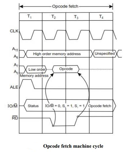
Fig 19. Timing diagram for op-code fetch cycle
Memory Read Machine Cycle:
The memory read cycle is executed by the processor to read a data byte from memory.
The machine cycle is exactly same to opcode fetch except:
a) It has three T-states
b) The S0 signal is set to 0.
The timing diagram of this cycle is given in

Fig 20. Timing diagram for memory read machine cycle
Memory Write Machine Cycle:
The memory write cycle is executed by the processor to write a data byte in a memory location. The processor takes three T-states and ^(WR) signal is made low. The timing diagram of this cycle is given in Figure.


I/O Read Cycle:
The I/O read cycle is executed by the processor to read a data byte from I/O port or from peripheral, which is I/O mapped in the system. The 8-bit port address is placed both in the lower and higher order address bus. The processor takes three T-states to execute this machine cycle. The timing diagram of this cycle is given in Figure
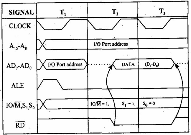
Fig 21. I/O read machine cycle
References:
- 8051 Microcontroller: An Applications Based Introduction Book by David Calcutt, Frederick J. Cowan, and Hassan Parchizadeh
- 8051 Microcontrollers: Internals, Instructions, Programming, and Interfacing Book by Subrata Ghoshal
- C and the 8051: Building efficient applications Book by Thomas W. Schultz
- MICROCONTROLLER Book by V. Udayashankara
- The 8051/8052 Microcontroller: Architecture, Assembly Language, and Hardware Interfacing Book by Craig Steiner