Unit - 2
Multiplexing and Baseband transmission
Multiplexing is the process of combining multiple signals into one signal, over a shared medium.
- The process is called as analog multiplexing if these signals are analog in nature.
- If digital signals are multiplexed, it is called as digital multiplexing.
Multiplexing was first developed in telephony. A number of signals were combined to send through a single cable. The process of multiplexing divides a communication channel into several number of logical channels, allotting each one for a different message signal or a data stream to be transferred. The device that does multiplexing, can be called as a MUX.
The reverse process, i.e., extracting the number of channels from one, which is done at the receiver is called as demultiplexing. The device which does demultiplexing is called as DEMUX.
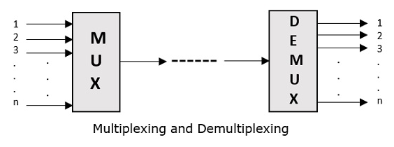
The following figures illustrates the concept of MUX and DEMUX. Their primary use is in the field of communications.
Types of Multiplexers
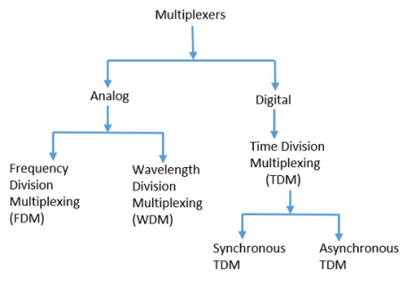
There are mainly two types of multiplexers, namely analog and digital. They are further divided into FDM, WDM, and TDM. The following figure gives a detailed idea about this classification.

There are many types of multiplexing techniques. Of them all, we have the main types with general classification, mentioned in the above figure. Let us take a look at them individually.
Analog Multiplexing
The analog multiplexing techniques involve signals which are analog in nature. The analog signals are multiplexed according to their frequency (FDM) or wavelength (WDM).
Frequency Division Multiplexing
In analog multiplexing, the most used technique is Frequency Division Multiplexing (FDM). This technique uses various frequencies to combine streams of data, for sending them on a communication medium, as a single signal.
Example − A traditional television transmitter, which sends a number of channels through a single cable uses FDM.
Wavelength Division Multiplexing
Wavelength Division multiplexing (WDM) is an analog technique, in which many data streams of different wavelengths are transmitted in the light spectrum. If the wavelength increases, the frequency of the signal decreases. A prism which can turn different wavelengths into a single line, can be used at the output of MUX and input of DEMUX.
Example − Optical fiber Communications use the WDM technique, to merge different wavelengths into a single light for the communication.
Digital Multiplexing
The term digital represents the discrete bits of information. Hence, the available data is in the form of frames or packets, which are discrete.
Time Division Multiplexing (TDM)
In TDM, the time frame is divided into slots. This technique is used to transmit a signal over a single communication channel, by allotting one slot for each message.
Of all the types of TDM, the main ones are Synchronous and Asynchronous TDM.
Synchronous TDM
In Synchronous TDM, the input is connected to a frame. If there are ‘n’ number of connections, then the frame is divided into ‘n’ time slots. One slot is allocated for each input line.
In this technique, the sampling rate is common for all signals and hence the same clock input is given. The MUX allocates the same slot to each device at all times.
Asynchronous TDM
In Asynchronous TDM, the sampling rate is different for each of the signals and a common clock is not required. If the allotted device, for a time slot transmits nothing and sits idle, then that slot is allotted to another device, unlike synchronous.
This type of TDM is used in Asynchronous transfer mode networks.
Demultiplexer
Demultiplexers are used to connect a single source to multiple destinations. This process is the reverse of multiplexing. As mentioned previously, it is used mostly at the receivers. DEMUX has many applications. It is used in receivers in the communication systems. It is used in arithmetic and logical unit in computers to supply power and to pass on communication, etc.
Demultiplexers are used as serial to parallel converters. The serial data is given as input to DEMUX at regular interval and a counter is attached to it to control the output of the demultiplexer.
Data Multiplexer
In digital electronics, multiplexers are also known as data selectors because they can “select” each input line, are constructed from individual Analogue Switches encased in a single IC package as opposed to the “mechanical” type selectors such as normal conventional switches and relays.
They are used as one method of reducing the number of logic gates required in a circuit design or when a single data line or data bus is required to carry two or more different digital signals. For example, a single 8-channel multiplexer.
Generally, the selection of each input line in a multiplexer is controlled by an additional set of inputs called control lines and according to the binary condition of these control inputs, either “HIGH” or “LOW” the appropriate data input is connected directly to the output. Normally, a multiplexer has an even number of 2n data input lines and a number of “control” inputs that correspond with the number of data inputs.
Note that multiplexers are different in operation to Encoders. Encoders are able to switch an n-bit input pattern to multiple output lines that represent the binary coded (BCD) output equivalent of the active input.
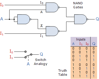
We can build a simple 2-line to 1-line (2-to-1) multiplexer from basic logic NAND gates as shown.
2-input Multiplexer Design
This technique allows to allot a fixed frequency band to every user in the complete channel bandwidth. Such frequency slot is allotted to each frequency user. The figure shows FDM below. The transmitter end contains multiple receivers and transmitters. The transmitter end sends a signal of different frequency. The transmtter1 sends signal of 30kHz, transmitter 2 sends signal of 40kHz and so on as shown below. These signals of different frequencies are multiplexed and transmitted.
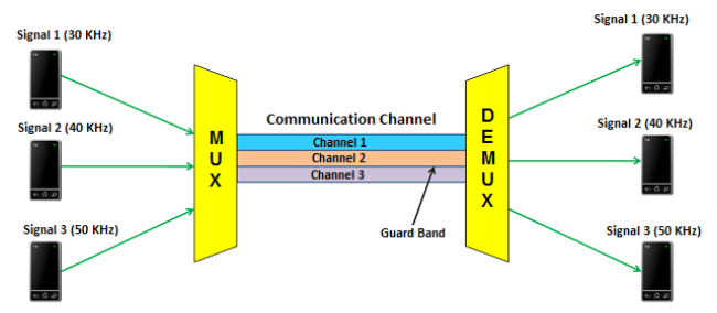
Fig: Frequency Division Multiplexing
At the receiver end, the multiplexed signals are separated by using a device called demultiplexer. It then sends the separated signals to the respective receivers. In the above figure, the receiver 1 receives signal of 30 kHz, receiver 2 receives signal of 40 kHz, and receiver 3 receives signal of 50 kHz.
Key takeaway
This technique allows to allot a fixed frequency band to every user in the complete channel bandwidth. Such frequency slot is allotted to each frequency user.
In TDM the complete channel bandwidth is allotted to one user for fixed time slot. For instance, if there are ten users then every user can be given the time slot of one second. Thus, complete channel can be used by each user for one second time in every ten seconds.
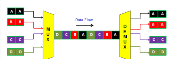
Fig: Time Division Multiplexing
This technique is suitable for digital signals because the digital signals are transmitted intermittently and the time spacing between two successive digital code words can be utilised by other signals. The TDM is classified in two types
S.No | FDM | TDM |
1 | The signals which are to be multiplexed are added in the time domain. But they occupy different slots in the frequency domain. | The signals which are to be multiplexed can occupy the entire bandwidth but they are isolated in the time domain. |
2.. | FDM is usually preferred for the analog signals | TDM is preferred for the digital signals.
|
3. | Synchronization is not required. | Synchronization is required. |
4. | The FDM requires a complex circuitry at the transmitter and receiver. | TDM circuitry is not very complex. |
5. | FDM suffers from the problem of crosstalk due to the imperfect band pass filters. | In TDM the problem of cross talk is not severe. |
6 | Due to wideband fading in the transmission medium, all the FDM channels are affected. | Due to fading only a few TDM channels will be affected. |
7 | Due to slow narrow band fading taking place in the transmission channel only a single channel may be affected in FDM. | Due to slow narrow band fading all the TDM channels may get wiped out. |
There are mainly two types of multiplexers, namely analog and digital. They are further divided into FDM, WDM, and TDM. The following figure gives a detailed idea about this classification.
Synchronous TDM
In synchronous time division multiplexing, each transmitter is allotted with a fixed time slot, regardless of the fact that the transmitter has any data to transmit or not. The device has to transmit data within this time slot. If the transmitter does not have any data to send then its time slot remains empty.
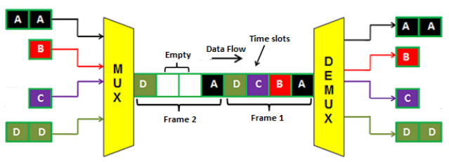
Fig: Synchronous TDM
The above figure shows four dedicated time slots A, B, C and D. The transmitter A data is sent at time slot A, transmitter B data is sent at time slot B, transmitter C data is sent at time slot C and transmitter D data is sent at time slot D.
In the time frame 2, the transmitter B and C does not have any data to send so the time slot B and C remains empty.
The main drawback of synchronous time division multiplexing is that the channel capacity is not fully utilized. Hence, the bandwidth goes wasted.
Asynchronous TDM
In this case the time slots are not fixed. The number of transmitters are not equal to the number of time slots. In asynchronous TDM the number of slots are always less than the transmitters.
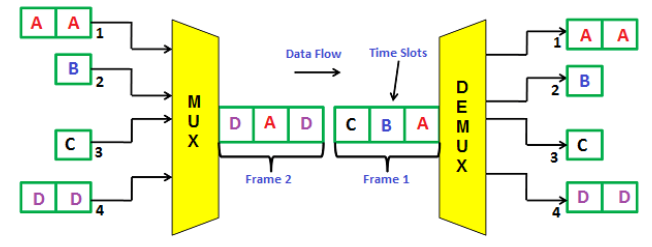
Fig: Asynchronous TDM
As seen from above figure the system has four transmitters and 3 time slots. Frame 1 is completely filled with data from devices A, B, C and D. Frame 1 has only 3 time slots. The data from D is filled in frame 2 in timeslot 1. The data from A and D are filled in timeslot 2 and 3 in time frame 2.
In asynchronous time division multiplexing, the multiplexer scans all the transmitters and accepts input only from the devices that have actual data to send and fills all the frames, and then sends it to the receiver. If there is not enough data to fill all the slots in a frame, then the partially filled frames are transmitted. In most of the cases, all the time slots in frames are completely filled.
Key takeaway
This technique is suitable for digital signals because the digital signals are transmitted intermittently and the time spacing between two successive digital codewords can be utilised by other signals
Pulse stuffing, often referred to as bit stuffing, is the practice of adding non-data bits to a binary signal before that signal is transmitted over a network. Pulse stuffing is often used as a means of controlling synchronization in systems that require both transmitter and receiver to transmit at the same bit rate. Alternatively, pulse stuffing can be used to make sure that the frames transmitted over a network conform to a standard size.
Working:
At their most basic level, network signals are transmitted as a string of zeros and ones. When a recipient receives this string, it interprets the zeros and ones as usable data. Pulse stuffing involves adding zeros or ones that are not part of the data being transmitted to this string. It is important that the receiving device knows what type of pulse stuffing is taking place before the signal is received, as receivers must strip out the stuffed bits in order to interpret the binary string correctly.
Bit Padding
Bit padding is a form of pulse stuffing whereby bits are added to a data packet to ensure that the packet is of a certain size. These bits are usually added to the end of the packet's useful data as a string of zeros or ones. Bit padding is used in protocols where packets have a fixed beginning and end, allowing systems to see where one packet starts and the next one ends.
Probability of Error defines average probability of error that can occur in a communication system.
Error Functions
(1) Error function erf(u):

(2) Complementary error function erfc(u):

Properties of Error function
1. Erf(-u) = -erf(u) - Symmetry.
2. Erf(u) approaches unity as u tends towards infinity.
3. For a Random variable X, with mean mx and variance σx2, the probability of X is defined by

Note: Relation: erfc(u) = 1 – erf(u) Tables are used to find these values.
Approximate value

Q – Function:
An alternate form of error function. It basically defines the area under the Standardized Gaussian tail. For a standardized Gaussian random variable X of zero mean and unit variance, the Q-function is defined by

Relations between Q-function and erfc function:


- The Integrate and Dump Filter (IDF) is used as a matched filter for the detection of signals in additive white Gaussian noise.
- The performance of the digital integrate and dump filter is evaluated.
- The case considered is when symbol times are known and the sampling clock is free running at a constant rate, i.e., the sampling clock is not phase locked to the symbol clock.
- Degradations in the output signal to noise ratio of the digital implementation due to sampling rate, sampling offset, and finite bandwidth, resulting from the anti-aliasing low pass prefilter, are computed and compared with those of the analog counterpart.
- It is shown that the digital IDF performs within 0.6 dB of the ideal analog IDF whenever the prefilter bandwidth exceeds four times the symbol rate and when sampling is performed at the Nyquist rate.
- The loss can be reduced to 0.3 dB by doubling the sampling rate, where 0.2 dB loss results from finite bandwidth and 0.1 dB results from the digital IDF
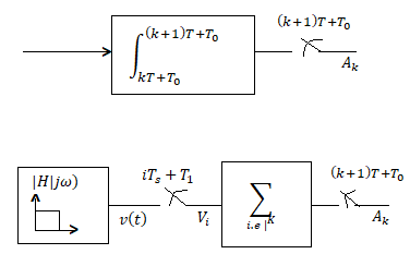
Fig: Integrate and dump filter
Key Takeaways:
The Integrate and Dump Filter (IDF) is used as a matched filter for the detection of signals in additive white Gaussian noise.
As discussed earlier that a noise interference may lead to wrong decision at the receiver end. As a matter of fact, the probability of error denoted by  is a good measure of performance of the detector.
We know that the output of the integrator is expressed as

For the positive pulse of amplitude A,  is given as
 or x(t) =A
Similarly, For the input pulse of amplitude -A,  is given as
 or x(t)=-A
Therefore, the output y(t) may be written as
x(t)= or x(t)=A (1)
Similarly, y(t)= or x(t)=-A (2)
Let us consider that x(t)=-A. Further if noise  is greater than, then the output y(t) would be positive according to equation (2). After that the receiver will decide in favour of symbol +A, which is wrong decision. This means that an error is introduced.
Similarly, let us consider that  If noise
  then, the output y(t) will be negative according to equation (1). This leads to decision in favour of –A, which is erroneous. Based on the above discussion we can make conclusions about probability of error in the form of a below table
Probability of error in integrate and dump filter receiver
S.No | Input x(t) | Value of  | The probability of error  |
1 | -A | An error will be introduced if  | In this case the probability of error may be obtained by calculating probability that  |
2 | +A | An error will be introduced if  | In this case the probability of error may be obtained by calculating probability that  |
An optimum filter is such a filter used for acquiring a best estimate of desired signal from noisy measurement. It is different from the classic filters. These filters are optimum because they are designed based on optimization theory to minimize the mean square error between a processed signal and a desired signal, or equivalently provides the best estimation of a desired signal from a measured noisy signal.
It is pervasive that when we measure a (desired) signal d(n), noise v(n) interferes with the signal so that a measured signal becomes a noisy signal
x(n) x(n)=d(n)+v(n)
It is also very common that a signal d(n) is distorted in its measurement (e.g., an electromagnetic signal distorts as it propagates over a radio channel). Assuming that the system causing distortion is characterized by an impulse response of h (n) s , the measurement of d(n) can be expressed by the sum of distorted signal s(n) and noise
v(n) x(n)=s(n)+v(n)= h (n)∗ s d(n)+v(n)
Where s(n)= h (n)∗ s d(n).
If both d(n) and v(n) are assumed to be wide-sense stationary (WSS) random processes, then x(n) is also a WSS process. The signals that we discuss in this chapter will be WSS if they are not specially specified. If signal d(n) and measurement noise v(n) are assumed to be uncorrelated (this is true in many practical cases), then r (k) = r (k) = 0.
In this case, the noisy signal,
x(n)= h (n)∗ s d(n)+v(n),
The relation of r (k) x with r (k ) d and r (k) v (the autocorrelations of x(n), d(n) and v(n), respectively) as follows,


For the noisy signal of the form x(n)= d(n)+v(n), a special case of where h (n) s =δ (n) and no distortion happens to d(n) in its measurement, we have


Optimum filtering is to acquire the best linear estimate of a desired signal from a measurement. The main issues in optimal filtering contain
• filtering that deals with recovering a desired signal d(n) from a noisy signal (or measurement) x(n);
• prediction that is concerned with predicting a signal d(n+m) for m>0 from observation x(n);
• smoothing that is an a posteriori form of estimation, i.e., estimating d(n+m) for m

Fig: Optimum filter
FSK Modulator
The FSK modulator block diagram comprises of two oscillators with a clock and the input binary sequence. Following is its block diagram.

Fig: FSK modulator
The two oscillators, producing a higher and a lower frequency signals, are connected to a switch along with an internal clock. To avoid the abrupt phase discontinuities of the output waveform during the transmission of the message, a clock is applied to both the oscillators, internally. The binary input sequence is applied to the transmitter so as to choose the frequencies according to the binary input.
FSK Demodulator
There are different methods for demodulating a FSK wave. The main methods of FSK detection are asynchronous detector and synchronous detector. The synchronous detector is a coherent one, while asynchronous detector is a non-coherent one.
Asynchronous FSK Detector
The block diagram of Asynchronous FSK detector consists of two band pass filters, two envelope detectors, and a decision circuit. Following is the diagrammatic representation.

Fig: FSK demodulator
The FSK signal is passed through the two Band Pass Filters BPFs, tuned to Space and Mark frequencies. The output from these two BPFs look like ASK signal, which is given to the envelope detector. The signal in each envelope detector is modulated asynchronously.
The decision circuit chooses which output is more likely and selects it from any one of the envelope detectors. It also re-shapes the waveform to a rectangular one.
GENERATION AND COHERENT DETECTION OF BPSK SIGNALS
(i) Generation
To generate the BPSK signal, we build on the fact that the BPSK signal is a special case of DSB-SC modulation. Specifically, we use a product modulator consisting of two components.
(i) Non-return-to-zero level encoder, whereby the input binary data sequence is encoded in polar form with symbols 1 and 0 represented by the constant-amplitude.
(ii) Product modulator, which multiplies the level encoded binary wave by the sinusoidal carrier of amplitude to produce the BPSK signal. The timing pulses used to generate the level encoded binary wave and the sinusoidal carrier wave are usually, but not necessarily, extracted from a common master clock.
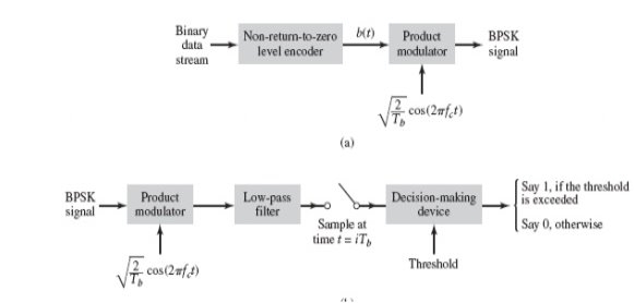
Fig: Product modulator

(ii) Detection
To detect the original binary sequence of 1s and 0s, the BPSK signal at the channel output is applied to a receiver that consists of four sections
(a)Product modulator, which is also supplied with a locally generated reference signal that is a replica of the carrier wave
(b)Low-pass filter, designed to remove the double-frequency components of the product modulator output (i.e., the components centered on) and pass the zero-frequency components.
(c)Sampler, which uniformly samples the output of the low-pass filter at where; the local clock governing the operation of the sampler is synchronized with the clock responsible for bit-timing in the transmitter.
(d)Decision-making device, which compares the sampled value of the low-pass filters output to an externally supplied threshold, every seconds. If the threshold is exceeded, the device decides in favour of symbol 1; otherwise, it decides in favour of symbol 0. Levels.

Fig: Decision-making device
The signal at (B) is


Fig: Decision-making device
GENERATION AND COHERENT DETECTION OF BFSK SIGNALS
(i) Generation
On-off level encoder:
Here, the output is of constant amplitude √Eb for input 1 and 0 for input 0.
Pair of oscillators:
Frequency f1 and f2 differ by integer multiple of 1/Tb. The lower oscillator has frequency f2 preceded by inverter. When in a signal interval, the input symbol is 1, the upper oscillator is switched on, and signal s1(t) is transmitted, while lower oscillator is switched off.
When input is 0, upper oscillator is off, lower oscillator is on and signal s2(t) is transmitted.
Again  , we see that the analysis for the case of simple (sampled) detection continues to apply, except that
- The value A must now be replaced by
 and
and - The value
 must be replaced by
The probability of error for matched filter detection is therefore

The polar binary case proceeds in the same way, except that the output of the matched filter is
 signal absent
 signal present
Once gain we can substitute 2E for A and  for
for  into the results for the simple case, so

Fig.12: BFSK generation
(ii) Detection
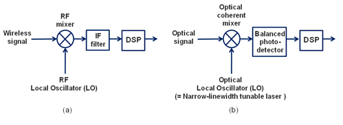
Fig: BFSK detection
It consists of two correlators with a common input, and reference signals Ø1(t), Ø2(t) are applied.
Then y = x1 – x2
The output y is compared with the threshold =0
If y>0 then output = 1 else 0.
But if y=0 then the receiver makes a random guess of 0 or 1.
Binary ASK
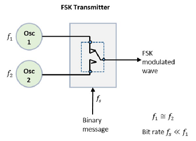
Fig: BASK Transmitter
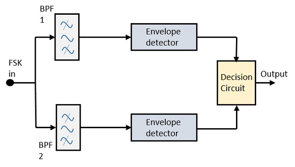
Fig: Coherent BASK Demodulation
In coherent binary ASK system the basic function is given by

The transmitted signals  and
and  are given by
 for symbol 1
 for symbol 0
The BASK system has one dimensional signal space with two messages
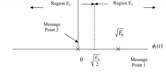
Fig: Signal Space Representation of BASK Signal
In transmitter the binary data sequence is given to an on-off encoder. Which gives an output  volts for symbol 1 and 0 volt for symbol 0. The resulting binary wave [in unipolar form] and sinusoidal carrier 1(t) is applied to a product modulator. The desired BASK wave is obtained at the modulator output. In demodulator, the received noisy BASK signal x(t) is apply to correlator with coherent reference signal 1(t) as shown in fig. (b). The correlator output x is compared with threshold λ.
If x > λ the receiver decides in favour of symbol 1.
If x < λ the receiver decides in favour of symbol 0.
Key Takeaways:
The FSK modulator block diagram comprises of two oscillators with a clock and the input binary sequence
The main methods of FSK detection are asynchronous detector and synchronous detector.
If a filter produces an output in such a way that it maximizes the ratio of output peak power to mean noise power in its frequency response, then that filter is called Matched filter.

Fig: Matched filter
Frequency Response Function of Matched Filter
The frequency response of the Matched filter will be proportional to the complex conjugate of the input signal’s spectrum. Mathematically, we can write the expression for frequency response function, H(f) of the Matched filter as −
H(f)=GaS∗(f)e−j2πft1 ………..1
Where,
Ga is the maximum gain of the Matched filter
S(f) is the Fourier transform of the input signal, s(t)
S∗(f) is the complex conjugate of S(f)
t1 is the time instant at which the signal observed to be maximum
In general, the value of Ga is considered as one. We will get the following equation by substituting Ga=1in Equation 1.
H(f)=S∗(f)e−j2πft1 ……..2
The frequency response function, H(f) of the Matched filter is having the magnitude of S∗(f)and phase angle of e−j2πft1, which varies uniformly with frequency.
Impulse Response of Matched Filter
In time domain, we will get the output, h(t) of Matched filter receiver by applying the inverse Fourier transform of the frequency response function, H(f).
 ….….3
….….3
Substitute, Equation 1 in Equation 3.

⇒ ………4
………4
We know the following relation.
S∗(f)=S(−f) ……..5
Substitute, Equation 5 in Equation 4.


⇒
In general, the value of Ga is considered as one. We will get the following equation by substituting Ga=1.
h(t)=s(t1−t)
The above equation proves that the impulse response of Matched filter is the mirror image of the received signal about a time instant t1. The following figures illustrate this concept.
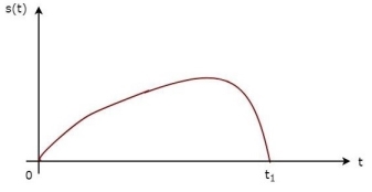

Fig: Impulse response of Matched filter
The received signal, s(t) and the impulse response, h(t) of the matched filter corresponding to the signal, s(t) are shown in the above figures.
Key Takeaways:
The frequency response function, H(f) of the Matched filter as −
H(f)=GaS∗(f)e−j2πft1 ………..1
Where,
Ga is the maximum gain of the Matched filter
S(f) is the Fourier transform of the input signal, s(t)
S∗(f) is the complex conjugate of S(f)
t1 is the time instant at which the signal observed to be maximum
Impulse response, h(t)=s( −t)
−t)
Impulse response, 
To yield the optimal formulation. The result of the convolution is then


Since  for t<0 and t>T. The output at t=T is then

Which is the required match filter value. Note also that subsequent samples also give the required integral for later bit intervals for t=2T.

When the input signal x(t) is identically the signal f(t) the output at t=T is

The energy of the signal. If the input signal is Gaussian white noise with PSD /2, then the PSD at the filter output is

The total output power over all frequencies is therefore

The output of the matched filter will be
 signal absent
 signal present
Here E is the energy in f(t), or

And  is the component due to noise. This quantity is a zero-mean random variable, and has a mean-square power(variance) equal to

Where is the noise power spectral density
Again defining y=y(T)
We see
That the analysis for the case of simple (sampled) detection continues to apply except that
The value A must now be replacaed by E, and
The value  must be replaced
The probability of error for matched filter detection is therefore

The polar binary case proceeds in the same way, except that he output of the matched filter is
 Signal absent
 signal present
Once gain we can substitute 2E for A and  into the results for the simple case so that

A regenerative repeater amplifies and reconstructs such a badly distorted digital signal and develops a nearly perfect replica of the original at its output. Regenerative repeaters are an essential key to digital transmission in that we could say that the "noise stops at the repeater."
Below is a simplified block diagram of a regenerative repeater and shows typical waveforms corresponding to each functional stage of signal processing. As illustrated in the figure, at the first stage of signal processing is amplification and equalization. With many regenerative repeaters, equalization is a two-step process. The first is a fixed equalizer that compensates for the attenuation-frequency characteristic (attenuation distortion), which is caused by the standard length of transmission line between repeaters (often 6000 ft or 1830 m). The second equalizer is variable and compensates for departures between nominal repeater section length and the actual length as well as loss variations due to temperature. The adjustable equalizer uses automatic line build-out (ALBO) networks that are automatically adjusted according to characteristics of the received signal.
The signal output of the repeater must be precisely timed to maintain accurate pulse width and space between the pulses. The timing is derived from the incoming bit stream. The incoming signal is rectified and clipped, producing square waves that are applied to the timing extractor, which is a circuit tuned to the timing frequency. The output of the circuit controls a clock-pulse generator that produces an output of narrow pulses that are alternately positive and negative at the zero crossings of the square-wave input.
The narrow positive clock pulses gate the incoming pulses of the regenerator, and the negative pulses are used to run off the regenerator. Thus the combination is used to control the width of the regenerated pulses.
Regenerative repeaters are the major source of timing jitter in a digital transmission system. Jitter is one of the principal impairments in a digital network, giving rise to pulse distortion and intersymbol interference.
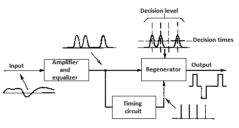
Fig. Regenerative Repeater
For synchronous transmission, data is not transferred byte-wise so there are no start or stop bits indicating the beginning or end of a character. Instead, there is a continuous stream of bits which have to be split up into bytes. Therefore the receiver has to sample the received data in the right instant and the sender's and receiver's clocks have to be kept in a synchronized state. As the main task lies in synchronizing sender's and receiver's clocks, bit synchronization is also called clock synchronization.
Clock encoding
The most self-evident way to accomplish clock synchronization is to send the clock signal to the receiver. This can be done by adding the signal of the local clock to the encoded signal of the bit stream resulting in a bipolar encoded signal which the receiver will have to interpret. By using this bipolar encoding, it is not necessary to create an additional transmission line just for the clock signal. Each bit span of the bipolar2 signal is dived in the middle by the signal shift of the clock. There are two possible values for each bit span: high-zero and low-zero, denoting logical one and logical zero. The received signal will contain enough information for the encoder as it can determine the length of a bit by the guaranteed signal change at the end of each bit and it can determine the literal value by distinguishing between a positive or negative signal in the first half of the bit time
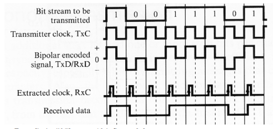
Fig: Clock encoding
Digital Phase-Locked Loop
The main idea of a digital phase locked loop is that the receiver's clock is reasonably accurate, but should be resynchronized with the sender's clock whenever possible. Unlike the direct clock encoding, there is no direct transmission of the clock signal, but it is possible to extract clock information from the received data signal. It is important that there are enough bit transitions in the received data stream which indicate bit boundaries and make it possible to deduct the duration of a bit time as well as enabling the clock controller to reset the clock to a less diverged signal. This can be ensured by using a bit scrambler which removes long sequences of zeros or one's, but a more convenient way is to use an encoding scheme which ensures a sufficient number of bit transitions like the Manchester encoding
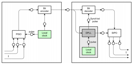
Fig: Manchester encoding
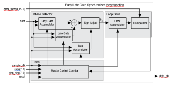
A system for deriving synchronizing pulses from a train of digital signals that is fed to in-phase and mid-phase gates each including an adder with delay feedback. The output of the mid phase gate is multiplied by a sign factor determined by a logic circuit connected to the in-phase gate. The output of the two gates is then mixed, filtered, and summed with a value dependent upon the clock rate and fed to a number-controlled oscillator which includes a counter and a comparing circuit. The output of the number-controlled oscillator is fed back to the in-phase and mid-phase gates.
The early/late gate synchronizer mega function contains all the functions necessary for a complete, first-order, closed-loop synchronizer. The synchronizer includes a phase detector, an up-down counter loop filter, and a digitally controlled oscillator (DCO). The phase detector is a balanced early/late gate, dual integrator design. The output of the phase detector is the difference, or phase error, between the data clock and the input data stream. The phase error (e) output from the phase detector is accumulated in an up-down counter, which increments and decrements according to the sign and magnitude of the phase error.
The DCO advances or retards the phase of the locally generated data clock whenever the error accumulator exceeds a specified error threshold. The error threshold is programmable and is used to control the bandwidth of the loop filter. The loop bandwidth can be narrowed by increasing the error threshold and widened by decreasing the error threshold. Small error thresholds allow the filter to respond to rapid changes in the phase error.
The DCO also adjusts the phase of the locally generated data clock in programmable step sizes. The step size, or magnitude, of the phase adjustment determines the loop acquisition time and data clock jitter. Large step sizes can be used to minimize acquisition times, since large phase steps can quickly correct large phase errors. Small step sizes can be used to minimize clock jitter when the loop is locked.
In modern computer networks data is not transferred as a simple stream of bits or bytes but in terms of frames or packets. This enables amongst other things packet based routing, error correction and the sharing of one physical medium between multiple clients. As the medium usually is a serial link and does not have a concept of frames or separated data units the sender and receiver have to recognize frame borders in the data stream on the medium. This process is called Frame Synchronization.
References:
1. B.P. Lathi, “Modern Digital and Analog communication Systems”, 4th Edition, Oxford University Press, 2010.
2. Rishabh Anand, Communication Systems, Khanna Publishing House, Delhi.
3. S.Haykin, Digital Communications, John Wiley & Sons, 2009.
4. B.Sklar, Digital Communications, 2 nd Edition, Pearson Education, New Delhi, 2009.
5. John G.Proakis, Digital Communications, 3 rd edition, McGraw Hill, 1995.