Unit – 2
8051 Assembly Language Programming
The next level of Programming Language is the Assembly Language. Since Machine Language or Code involves all the instructions in 1’s and 0’s, it is very difficult for humans to program using it.
Assembly Language is a pseudo-English representation of the Machine Language. The 8051 Microcontroller Assembly Language is a combination of English like words called Mnemonics and Hexadecimal codes.
It is also a low level language and requires extensive understanding of the architecture of the Microcontroller.
Each line or statement of the assembly language program of 8051 Microcontroller consists of three fields: Label, Instruction and Comments.

Label
The Label is programmer chosen name for a Memory Location or a statement in a program. The Label part of the statement is optional and if present, the Label must be terminated with a Colon (:).
Instruction
The Instruction is the main part of the 8051 Microcontroller Assembly Language Programming as it is responsible for the task performed by the Microcontroller.
Comment
Comments are statements included by the developer for easier understanding of the code and is used for proper documentation of the Program.
The steps to create an executable Assembly language program are outlined as follows.
- First, we use an editor to type in a program. Many editors or word processors are available that can be used to create and/or edit the program. The most widely used editor is MS-DOS EDIT program or Notepad in Windows which comes with all Microsoft operating systems.
Note: the editor must be able to produce an ASCII file. For many assemblers, the file names follow the usual DOS conventions, but the source file has the extension “asm” or “src”, depending on which assembler you are using.
2. The “asm” source file containing the program code created in step 1 is fed to an 8051 assembler. The assembler converts the instructions into machine code. The assembler will produce an object file and list file. The extension for object file is “obj” while the extension for list file is “1st”.
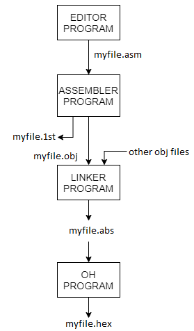
Figure. Steps to create a program
3. Assemblers require a third step called linking. The link program takes one or
more object files and produces an absolute object file with the extension “abs”
4. Next, the “abs” file is fed into a program called “OH” object to hex convert
er which creates a file with extension “hex” that is ready to burn into ROM.
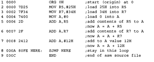
8051 addressing modes are classified as follows.
- Immediate addressing.
- Register addressing.
- Direct addressing.
- Indirect addressing.
- Relative addressing.
- Absolute addressing.
- Long addressing.
- Indexed addressing.
- Bit inherent addressing.
- Bit direct addressing.
Immediate addressing:
In this addressing mode the data is provided as a part of instruction itself.
That is the data immediately follows the instruction.
E.g., MOV A, #30H;
ADD A, #83;
Here # Symbol indicates that data is immediate.
Register addressing:
In this addressing mode the register will hold the data.
One of the eight general registers (R0 to R7) is used and specified as the operand.
E.g., MOV A, R0;
ADD A, R6
R0 – R7 will be selected from the current selection of register bank. The default register bank will be bank 0.
Direct addressing:
There are two ways to access the internal memory that is by using direct address and indirect address.
In direct addressing mode we not only address the internal memory but SFRs also.
In direct addressing, an 8-bit internal data memory address is specified as part of the instruction and hence, it can specify the address only in the range of 00H to FFH.
In this addressing mode, data is obtained directly from the memory.
E.g., MOV A,60h
ADD A,30h
Indirect addressing:
The indirect addressing mode uses a register to hold the actual address that is used in data movement.
Registers R0 and R1 and DPTR are the only registers that can be used as data pointers.
Indirect addressing cannot be used to refer to SFR registers.
Both R0 and R1 can hold 8-bit address and DPTR can hold 16-bit address.
E.g., MOV A, @R0
ADD A, @R1
MOVX A, @DPTR
Indexed addressing:
In indexed addressing, either the program counter (PC), or the data pointer (DTPR)—is used to hold the base address, and A is used to hold the offset address.
Adding the value of the base address to the value of the offset address forms the effective address.
Effective address = Base address + value of offset address.
Indexed addressing is used with JMP or MOVC instructions.
Look up tables are easily implemented with the help of index addressing.
E.g., MOVC A, @A+DPTR // copies the contents of memory location pointed by the sum of the accumulator A and the DPTR into accumulator A.
MOVC A, @A+PC // copies the contents of memory location pointed by the sum of the accumulator A and the program counter into accumulator A.
Relative Addressing:
Relative addressing is used only with conditional jump instructions. The relative address, (offset), is an 8-bit signed number, which is automatically added to the PC to make the address of the next instruction.
The 8-bit signed offset value gives an address range of +127 to —128 locations.
The jump destination is usually specified using a label and the assembler calculates the jump offset accordingly.
The advantage of relative addressing is that the program code is easy to relocate and the address is relative to position in the memory.
E.g., SJMP LOOP1 JC BACK
Absolute addressing:
Absolute addressing is used only by the AJMP (Absolute Jump) and ACALL (Absolute Call) instructions.
These are 2 bytes instructions.
The absolute addressing mode specifies the lowest 11 bit of the memory address as part of the instruction.
The upper 5 bit of the destination address are the upper 5 bit of the current program counter. Hence, absolute addressing allows branching only within the current 2 Kbyte page of the program memory.
E.g., AJMP LOOP1 ACALL LOOP2
Long Addressing:
The long addressing mode is used with the instructions LJMP and LCALL. These are 3-byte instructions. The address specifies a full 16-bit destination address so that a jump or a call can be made to a location within a 64 Kbyte code memory space.
E.g., LJMP FINISH LCALL DELAY
Bit Inherent Addressing:
In this addressing, the address of the flag which contains the operand, is implied in the opcode of the instruction.
E.g., CLR C; Clears the carry flag to 0
Bit Direct Addressing:
In this addressing mode the direct address of the bit is specified in the instruction. The RAM space 20H to 2FH and most of the special function registers are bit addressable. Bit address values are between 00H to 7FH.
E.g., CLR 07h; Clears the bit 7 of 20h RAM space
SETB 07H; Sets the bit 7 of 20H RAM space.
Key Takeaways
Addressing mode is a way to address an operand. Operand means the data we are operating upon.
Data Transfer Instructions
The Data Transfer Instructions relate to transfer of data between registers or external program memory or data memory. The Mnemonics associated with Data Transfer are given below.
- MOV
- MOVC
- MOVX
- PUSH
- POP
- XCH
- XCHD
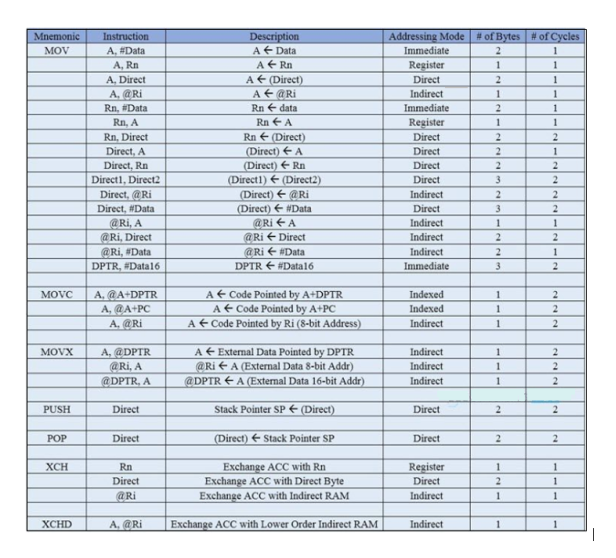 |
Arithmetic Instructions
Using Arithmetic Instructions, one can perform addition, subtraction, multiplication and division. It consists of increment by one, decrement by one and a special instruction called Decimal Adjust Accumulator.
The Mnemonics associated with the Arithmetic Instructions of the 8051 Microcontroller Instruction Set are:
- ADD
- ADDC
- SUBB
- INC
- DEC
- MUL
- DIV
- DA A
The arithmetic instructions have no knowledge about the data format that is signed, unsigned, ASCII, BCD, and so on. The operations performed by the arithmetic instructions affect flags like carry, overflow, zero, etc. in PSW Register.
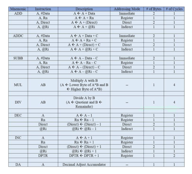 |
Logical Instructions
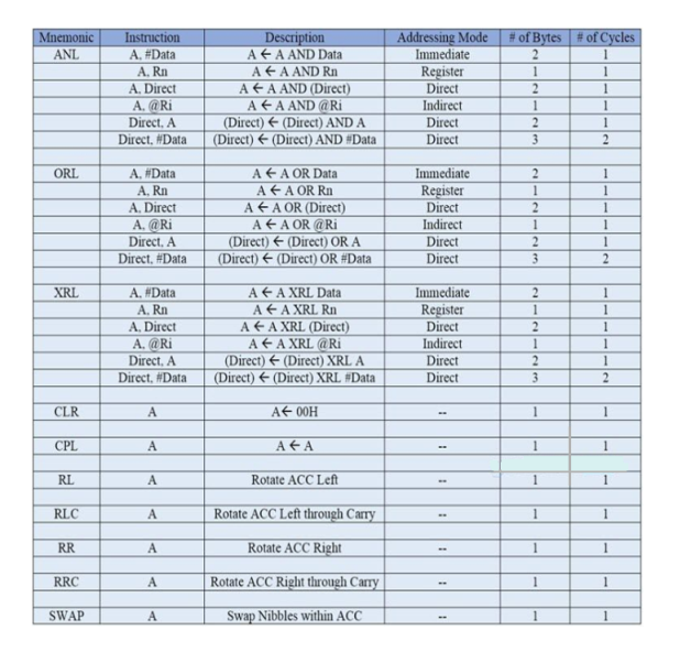
Logical Instructions perform logical operations like AND, OR, XOR, NOT, Rotate, Clear and Swap. Logical Instruction are performed on bytes of data on a bit-by-bit basis.
Mnemonics associated with Logical Instructions are as follows:
- ANL
- ORL
- XRL
- CLR
- CPL
- RL
- RLC
- RR
- RRC
- SWAP
 |
Bit Manipulation Instructions
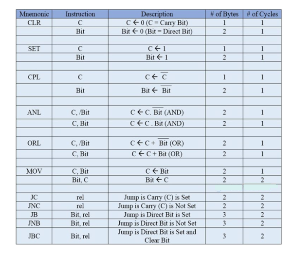
Boolean or Bit Manipulation Instructions will deal with bit variables. There is a special bit-addressable area in RAM and some Special Function Registers (SFRs) that are bit addressable.
The Mnemonics corresponding to the Boolean or Bit Manipulation instructions are:
- CLR
- SETB
- MOV
- JC
- JNC
- JB
- JNB
- JBC
- ANL
- ORL
- CPL
These instructions perform set, clear, and, or, complement at bit level. All the possible mnemonics of the Boolean Instructions are specified in the following table.
 |
Program Branching Instructions
The logic of the program is controlled by these instructions. The mnemonics of the Program Branching Instructions are :
- LJMP
- AJMP
- SJMP
- JZ
- JNZ
- CJNE
- DJNZ
- NOP
- LCALL
- ACALL
- RET
- RETI
- JMP
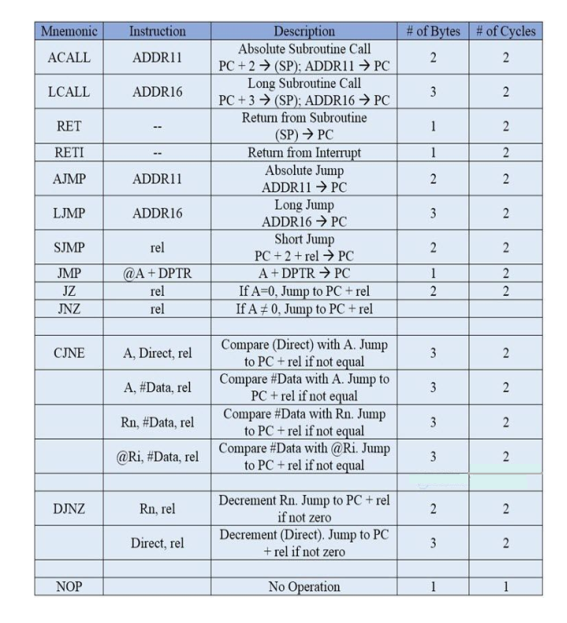
All these instructions, except the NOP (No Operation) affect the Program Counter (PC) Some of these instructions have decision making capability before transferring control to other part of the program.
The following table shows all the mnemonics with respect to the program branching instructions.
 |
Using Arithmetic Instructions, one can perform addition, subtraction, multiplication and division. It consists of increment by one, decrement by one and a special instruction called Decimal Adjust Accumulator.
The Mnemonics associated with the Arithmetic Instructions of the 8051 Microcontroller Instruction Set are:
The arithmetic instructions have no knowledge about the data format that is signed, unsigned, ASCII, BCD, and so on. The operations performed by the arithmetic instructions affect flags like carry, overflow, zero, etc. in PSW Register.
Mnemonic | Instruction | Description | Addressing Mode |
ADD | A, #data | A <- A + Data | Immediate |
| A, Rn | A<- A + Rn | Register |
| A, Direct | A<- A + (Direct) | Direct |
| A, @Ri | A<- A + @Ri | Indirect |
|
|
|
|
ADDC | A, #data | A <- A + Data + C | Immediate |
| A, Rn | A<- A + Rn + C | Register |
| A, Direct | A<- A + (Direct)+C | Direct |
| A, @Ri | A<- A + @Ri +C | Indirect |
|
|
|
|
SUBB | A, #data | A <- A – Data | Immediate |
| A, Rn | A<- A- Rn | Register |
| A, Direct | A<- A - (Direct) | Direct |
| A, @Ri | A<- A XRL-Ri | Indirect |
|
|
|
|
MUL AB | Multiply A with B |
|
|
|
|
|
|
DIV AB | Divide A by B |
|
|
|
|
|
|
DEC A | A, #data | A <- A -1 |
|
| A, Rn | Rn <-Rn -1 |
|
| A, Direct | (Direct) <- (Direct) -1 |
|
| A, @Ri | @Ri<- @Ri -1 |
|
INC A | A, #data | A <- A+1 |
|
| A, Rn | Rn <-Rn +1 |
|
| A, Direct | (Direct)<- (Direct) +1 |
|
| A, @Ri | @Ri<- @Ri+1 |
|
DAA | A | Decimal Adjust Accumulator |
|
Logical Instructions perform logical operations like AND, OR, XOR, NOT, Rotate, Clear and Swap. Logical Instruction are performed on bytes of data on a bit-by-bit basis.
Mnemonics associated with Logical Instructions are as follows:
Mnemonic | Instruction | Description | Addressing Mode |
ANL | A, #data | A <- A AND Data | Immediate |
| A, Rn | A<- A AND Rn | Register |
| A, Direct | A<- A AND (Direct) | Direct |
| A, @Ri | A<- A AND @Ri | Indirect |
| Direct A | (Direct) <- (Direct) AND A | Direct |
| Direct, # Data | (Direct) <- (Direct) AND # Data | Direct |
|
|
|
|
ORL | A, #data | A <- A OR Data | Immediate |
| A, Rn | A<- A OR Rn | Register |
| A, Direct | A<- A OR (Direct) | Direct |
| A, @Ri | A<- A OR @Ri | Indirect |
| Direct A | (Direct) <- (Direct) OR A | Direct |
| Direct, # Data | (Direct) <- (Direct) OR # Data | Direct |
|
|
|
|
XRL | A, #data | A <- A XRL Data | Immediate |
| A, Rn | A<- A XRL Rn | Register |
| A, Direct | A<- A XRL (Direct) | Direct |
| A, @Ri | A<- A XRL @Ri | Indirect |
| Direct A | (Direct) <- (Direct) XRL A | Direct |
| Direct, # Data | (Direct) <- (Direct) XRL # Data | Direct |
|
|
|
|
CLR | A | A<-00H |
|
CPL | A | A<-A |
|
|
|
|
|
RL | A | Rotate ACC Left |
|
|
|
|
|
RLC | A | Rotate ACC Left through carry |
|
RR | A | Rotate ACC right |
|
|
|
|
|
RRC | A | Rotate ACC right through carry |
|
SWAP | A | Swap nibbles within ACC |
|
ORG 8000H
MOV R0, #0FH
MOV R1, #FOH
MOV R2, #66H
; AND OPERATION
MOV A, #FFH
ANL A, R0
MOV R3, A
; OR OPERATION
MOV A, #FFH
ORL A, R1
MOV R4, A
; XOR OPERATION
MOV A, 03H
MOV A, #FFH
XRL A, R2
MOV R5, A
LCALL 0003H
END
ORG 9000H
; CLEAR REGISTER A
MOV A, #0FH
CLR A
MOV R0, A
; SWAP NIBBLES OF REGISTER A
MOV A, #56H
SWAP A
MOV R1, A
; COMPLEMENT THE BIT OF REGISTER A
MOV A, #66H
CPL A
MOV R2, A
; ROTATE THE REGISTER CONTENTS TOWARDS RIGHT
MOV A, #63H
RR A
XRL A, R
MOV R3, A
; ROTATE THE REGISTER CONTENTS TOWARDS LEFT
MOV A, #43H
RL A
XRL A, R
MOV R4, A
LCALL 0003H
END
JZ label; Jump if A=0
JNZ label; Jump if A! =0
DJNZ reg, label; Decrement and Jump if A (or reg.)! =0
CJNE A, byte; Compare and Jump if A! =byte
CJNE reg, #data; Compare and Jump if byte! =data
JC; Jump if Carry=1 J
NC; Jump if Carry=0
JB; Jump if bit =1
JNB; Jump if bit =0
JBC; Jump if bit=1 and clear bit
LCALL: 3-byte instruction • When subroutine is called – Control is transferred to that subroutine – Processor saves the PC onto the Stack and begins to fetch instructions from new location. – RET (return to caller) POP from Stack to PC.
ACALL:
2-byte instruction
ACALL’s target address must be with in a 2KB range
Write a program to clear Accumulator [A], then Add 5 to the accumulator 20 times:
Answer:
This program adds value 3 to the Accumulator 20 times
MOV A, #0; Accumulator=0, Clear Accumulator
MOV R2, #20; Load counter R2=20
AGAIN: ADD A, #05; Add 05 to Accumulator
DJNZ R2, AGAIN; Repeat Until R2=0 [20 times]
MOV R5, A; Save Accumulator in R5
There are four ports in 8051 microcontroller named as P0, P1, P2 and P3. Each port has 8 pins. For Port 0 8 pins names as P0.0, P0.1, P0.2, P0.3, P0.4, P0.5, P0.6, and P0.7. All the ports upon RESET are ready to be configured or used as output. To use all these ports as an input port, it must be programmed.
PORT 0:
Port 0 has 8 pins P0.0, P0.1, P0.2, P0.3, P0.4, P0.5, P0.6, and P0.7, pins 39, 38, 37, 36, 35, 34, 33, 32. This port can be used for input or output. Each pin of the port 0 must be connected externally to a 10K Ohm pull-up resistor, to use Port 0 as both input or output ports. This is because the Port 0 [P0] is an open drain. This is not the case in other ports P1, P2 and P3. 'Open drain' is a term used for MOS chips, as 'open collector' is used for TTL chips. To use Port 0 for both input and output, have to connect Port 0 to pull-up resistors. When external pull-up resistors connected upon reset, Port 0 is configuring as output port.
Role of Port 0 as Input Port:
To make Port 0 as input port, the pull up resistors are connected to port 0. The port must be programmed by writing 1 to all the bits. Let’s examine the code example below in which the Port 0 is configured first as an input port by writing 1's to it and then data is received from that port and send to Port 1 [P1].
MOV A, #0FFH; Load accumulator with value FFH in hex or 255 in decimal
MOV P0, A; Make Port 0 as an input port by writing all 1's to it
BACK: MOV A, P0; Get data from Port 0
MOV P1, A; Send it to Port 1
SJMP BACK; Keep doing it repeatedly
The Dual Role of Port 0:
Port 0 can be used to configures for both data and address. The Port 0 is also designated as AD0 - AD7. When connecting an 8051 to an external memory, port 0 provides both address and data. The 8051 multiplexes address and data through Port 0 to save pins. Address latch enable [ALE] indicates if Port 0 has address or data. When ALE=0, it provides data D0 - D7, but when ALE = 1, it has address A0 - A7. With the help of 74LS373 latch, ALE is used for demultiplexing address and data.
PORT 1:
Port 1 has a total of 8 pins. P1.0, P1.1, P1.2, P.13, P1.4, P1.5, P1.6, and P1.7. Port 1 can be used as an input or output. As compares to Port 0, this port does not need any pull-up resistors. Port 1 already has internally connected pull-up resistors. Port 1 is configured as an output port when reset.
Example # 1:
Let’s examine the code, which will continuously send Output to Port 1 the alternating values 55H and AAH
MOV A, #55H
BACK MOV P1, A
ACALL DELAY
CPL A
SJMP BACK
The Role of Port 1 as Input Port:
The Port 1 must be programmed by writing 1's to all the bits in order to make Port 1 as an input port.
Example # 2:
MOV A, #0FFH; Load Accumulator with FFH in hex
MOV P1, A; Make P1 an input Port, by writing all 1's to Port 1
MOV A, P1; Get data from Port 1
MOV R3, A; Save data in register R3
ACALL DELAY; Wait
MOV A, P1; Get another data from Port 1
MOV R4, A; Save data in register R4
ACALL DELAY; Wait
MOV A, P1Get another data from Port 1
MOV R5, A; Save data in register R5
In Example # 2 above, the Port 1 is configured as input port by writing 1's to it, then data is received from that port and saved in R3, R4 and R5.
PORT 2:
Port 2 also has total of 8 pins. P2.0, P2.1, P2.2, P2.3, P2.4, P2.5, P2.6, and P2.7. Port 2 can be used for input or output port. To make Port 2 as an input, the Port 2 must be programmed by writing 1's to all bits.
Example # 3:
MOV A, #55H
BACK: MOV P2, A
ACALL DELAY
CPL A
SJMP BACK
In Example # 3 above, the code will send out continuously to Port 2 an alternating values 55H and AAH to toggle the bits or Port 2 continuously.
The Role of Port 2 as an Input Port:
The Port 2 must be programmed by writing 1's to all the port 2 bits to make Port 2 as an input port.
Example #4:
MOV A, #0FFH; Load accumulator with value 0FFH in hex
MOV P2, A; Make Port 2 an input port by writing 1's to all bits of port 2
BACK: MOV A, P2; Get data from Port 2
MOV P1, A; Send data to Port 1
SJMP BACK; Keep doing it repeatedly
In Example # 4 above, the Port 2 is configured as input port by writing all 1's, then data is received from that port and is sent to Port 1 continuously.
The Dual Role or Port 2:
Port 2 has dual role. Port 2 is also designated as A8 - A15. This indicates that Port 2 has a dual function. An 8031 microcontroller is capable of accessing 64K bytes of external memory, it needs a path for the 16 bits of the address. P0 provides the lower 8 bits via A0 - A7 while Port 2 provides bits A8 - A15 of the address. When the 8031 is connected to external memory, Port 2 is used for the upper 8 bits of the 16-bit address, and it cannot be used for input / output operations.
Port 3:
Port 3 has total 8 Pins. P3.0, P3.1, P3.2, P3.3, P3.4, P3.5, P3.6, and P3.7. Pins 10, 11, 12, 13, 14, 15, 16, and 17. Port 3 can be sued as an input port or output port. Port 3 does need any pull-up resisters, just like the Port 1 and Port 2 does not require pull-up resistors. Only Port 0 require Pull-up resistors. Port 3 configured as an output port upon system reset. Port 3 has additional function of providing signals of interrupts.
Alternate Functions of Port 3:
PORT 3 BIT FUNCTION PIN
P3.0 RxD [Receive Serial Communications Signals] 10
P3.1 TxD [Transmit Serial Communications Signals] 11
P3.2 INT0 [External Interrupt 0] 12
P3.3 INT1 [External Interrupt 1] 13
P3.4 T0 [Timer 0] 14
P3.5 T1 [Timer 1] 15
P3.6 WR [Write Signals of External Memory] 16
P3.7 RD [Read Signals of External Memory] 17
The Carry Flag (CY) acts like the single-bit accumulator in different bit processing instructions.
In the following table, we will see the Mnemonics, Lengths, Execution Time in terms of the machine cycle, Number of Opcodes etc.
Mnemonics | Byte Count | Execution Time | Opcode Count |
CLR C | 1 | 1 | 1 |
ADD A, Rn | 1 | 1 | 8 |
SETB C | 1 | 1 | 1 |
ADD A, @Ri | 1 | 1 | 2 |
CPL C | 1 | 1 | 1 |
ADDC A, Rn | 1 | 1 | 8 |
SUBB A, Rn | 1 | 1 | 8 |
SUBB A, @Ri | 1 | 1 | 2 |
Examples
Sr.No | Instruction & Description |
1 | CLR C |
2 | CPL C |
In order to program 8051 timers, it is important to know the calculation of initial count value to be stored in the timer register.
The calculations are as follows. In any mode,
Timer Clock period = 1/Timer Clock Frequency. = 1/ (Master Clock Frequency/12)
- Mode 1 (16-bit timer/counter) Value to be loaded in decimal = 65536 – (Delay Required/Timer clock period). Convert the answer into hexadecimal and load onto THx and TLx register. (65536D = FFFFH+1).
- Mode 0 (13-bit timer/counter) Value to be loaded in decimal = 8192 – (Delay Required/Timer clock period) Convert the answer into hexadecimal and load onto THx and TLx register. (8192D = 1FFFH+1)
c. Mode 2 (8 bit auto reload) Value to be loaded in decimal = 256 – (Delay Required/Timer clock period) Convert the answer into hexadecimal and load onto THx register.
Upon starting the timer this value from THx will be reloaded to TLx register. (256D = FFH+1)
Steps for programming timers in 8051
Mode 1:
Load the TMOD value register indicating which timer (0 or 1) is to be used and which timer mode is selected. Load registers TL and TH with initial count values.
- Start the timer by the instruction “SETB TR0” for timer 0 and “SETB TR1” for timer 1.
- Keep monitoring the timer flag (TF) with the “JNB TFx, target” instruction to see if it is raised. Get out of the loop when TF becomes high.
- Stop the timer with the instructions “CLR TR0” or “CLR TR1”, for timer 0 and timer 1, respectively.
- Clear the TF flag for the next round with the instruction “CLR TF0” or “CLR TF1”, for timer 0 and timer 1, respectively.
- Go back to step 2 to load TH and TL again.
Mode 0:
The programming techniques mentioned here are also applicable to counter/timer mode 0. The only difference is in the number of bits of the initialization value.
Mode 2:
- Load the TMOD value register indicating which timer (0 or 1) is to be used; select timer mode
- Load TH register with the initial count value. As it is an 8-bit timer, the valid range is from 00 to FFH.
- Start the timer. Keep monitoring the timer flag (TFx) with the “JNB TFx, target” instruction to see if it is raised.
- Get out of the loop when TFx goes high. Clear the TFx flag.
- Go back to step 4, since mode 2 is auto-reload.
Write an 8051 C program to toggle only pin PI.5 continuously every 250 ms. Use Timer 0, mode 2 (8-bit auto-reload) to create the delay.
Solution:
#include<reg51.h>
Void TOM2Delay(void);
Sbit mybit=P1^5;
Void mian(void)
{
Unsigned char x,y;
While(1)
{
Unsigned char x,y;
While(1)
{
Mybit= ˜ mybit;
For(x=0;x<250;x++)
For(y=0;y<36;y++)
TOM2Delay();
}
}
256-23 = 233
23 x 1.085 us = 25 us
25 us x 250 x 40 = 250 ms by calculation.
However, the scope output does not give us this result. This is due to overhead of the for loop in C. To correct this problem, we put 36 instead of 40.
Write an 8051 C program to create a frequency of 2500 on pin P2.7. Use Timer 1 mode 2 to create delay.
# include<reg51.h>
Void T1M2Delay(void);
Sbit mybit= P2^7;
Void main(void)
{
Unsigned char x;
While(1)
{
Mybit= ˜ mybit;
T1M2Delay();
}
}
Void TIM2Delay(void)
TMOD = 0x20;
TH1=184;
TR1=1;
While(TF1==0);
TR1=0;
TF1=0;
}
1/2500 Hz = 400μs
400μs/2 = 200μs
200μs/1.085μs= 184
Key Takeaways
A timer is a clock that controls the sequence of an event while counting in fixed intervals of time. It is used to repeat or initiate an action after/at a known period of time.
STEPS TO PROGRAM COUNTERS AND PRINT COUNTS IN LCD:
- Initialize the TMOD register to make it timer/counter function as a register.
- We are using only mode 1 of Timer0 so our TMOD hex value will be 0x05.
- Load the Initial value from where your counter needs to be start counting TL0=0.
- Start the Timer 0 to start counting by feeding the logic 1 to it TR0=1.
- To display the count values in LCD copy the TL0 values to a Integer, in our program we used ” val “.
- The LCD cannot display a integer , so we need to convert the integer to character.
- For that purpose we use ” sprintf(ch,”%u”,val); “
- This will convert the Integer ” val ” values to character “ch”.
- Feed the Character “ch” for displaying it in LCD.
CODE:
#include<regx51.h>
#include<stdio.h>
Sbit rs=P3^5;
Sbit rw=P3^6;
Sbit en=P3^7;
Void lcd(char a,int b); //subroutine for lcd display
Unsigned char msg[]="Count";
Char ch[4];
Void delay(); //sub routine for delay
Void counter(); //subroutine for counters
Int k;
Unsigned int val;
Void main()
{
Lcd(0x38,0);
Lcd(0x0c,0);
Lcd(0x80,0);
TMOD=0x05; //selecting counter mode
Counter();
}
Void delay()
{
Int i;
For(i=0;i<=2000;i++); //software delay
}
Void counter()
{
TL0=0; //lodaing initial value
TR0=1; //starting timer
For(k=0;k<5;k++)
{
Lcd(msg[k],1);
}
While(1)
{
Lcd(0x86,0); //setting fixed position
Val=TL0|TH0<<8; //shifting the values from TL0 to TH0
Sprintf(ch,"%u",val); //conversion of integer to character
For(k=0;k<5;k++)
{
Lcd(ch[k],1);
}
}
}
Void lcd(char a,int b)
{
P1=a;
Rs=b;
Rw=0;
En=1;
Delay();
En=0;
Delay();
}
References:
- Microprocessor Architecture, Programming, and ...Book by Ramesh S. Gaonkar
- 8085 Microprocessor: Programming and Interfacing Book by N. K. Srinath
- 8085 Microprocessors & Its Application Book by Nagoorkani
- C and the 8051: Building efficient applications Book by Thomas W. Schultz
- MICROCONTROLLER Book by V. Udayashankara