Unit - 4
Hardware Interfacing
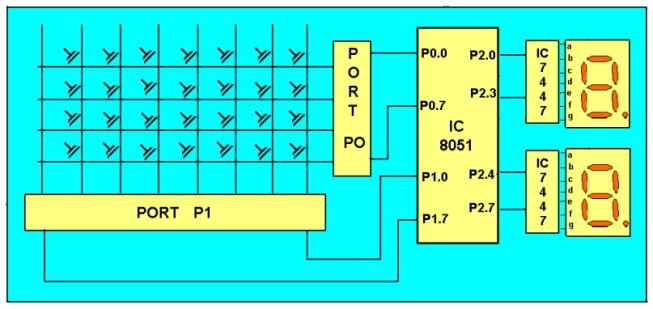
Fig.1: Keyboard Interfacing with 8051
Working:
❖ The 8051 has 4 I/O ports P0 to P3 each with 8 I/O pins, P0.0 to P0.7, P1.0 to P1.7, P2.0 to P2.7, P3.0 to P3.7. Port P1 acts as an I/P port for microcontroller and port P0 as an O/P port, Port P2 is used for displaying the number of pressed keys.
❖ Make all rows of port P0 high so that it gives a high signal when key is pressed.
❖ Check if any key is pressed by scanning port P1 by checking all the columns for non- zero condition.
❖ If any key is pressed, identify which key is pressed and make one row high at a time.
❖ Initiate a counter to hold the count so that each key is counted.
❖ Check port P1 for nonzero condition. If any nonzero number is there in [accumulator], start column scanning by following step 9.
❖ Otherwise make the next row high in port P1.
❖ Add a count of 08h to the counter to move to the next row by repeating steps from step 6.
❖ If any key pressed is found, the [accumulator] content is rotated right through the carry until carry bit sets, while doing this increment count in the counter till carry is found.
❖ Move the content in the counter to display in data field or to memory location
❖ To repeat the procedures, go to step 2.
Program:
Start of main program:
To check that whether any key is pressed
Start: mov a, #00h
Mov p1, a; making all rows of port p1 zero
Mov a, #0fh
Mov p1, a; making all rows of port p1 high
Press: mov a, p2
Jz press; check until any key is pressed
After making sure that any key is pressed
Mov a, #01h; make one row high at a time
Mov r4, a
Mov r3, #00h; initiating counter
Next: mov a, r4
Mov p1, a; making one row high at a time
Mov a, p2; taking input from port A
Jnz colscan; after getting the row jump to check
Column
Mov a, r4
Rl a; rotate left to check next row
Mov r4, a
Mov a, r3
Add a, #08h; increment counter by 08 count
Mov r3, a
Sjmp next; jump to check next row
After identifying the row to check the column following steps are followed
Colscan: mov r5, #00h
In: rrc a; rotate right with carry until get the carry
Jc out; jump on getting carry
Inc r3; increment one count
Jmp in
Out: mov a, r3
Da a; decimal adjust the contents of counter
Before display
Mov p2, a
Jmp start; repeat for check next key.
Light Emitting Diodes are considered as semi- conductor light sources. The commonly used LEDs have a cut-off voltage of 1.7V and current of 10mA. When applied with its required voltage and current it glows with full intensity.
The Light Emitting Diode works similar to normal PN- diode but it emits energy in the form of light. The color of the light depends on the semiconductors band gap.

Figure 2. LED
LED is connected to AT89C51 microcontroller with the current limiting resistor. The value of this resistor is calculated using the following formula.
R= (V-1.7)/10mA, where V is the input voltage.
The maximum output voltage of microcontrollers is 5V. Hence the calculated value of resistor is 330 Ohms. The resistor can be connected to cathode or the anode of LED.
- Initially, burn the code into the microcontroller.
- Connect the LEDs to the Port0 of the microcontroller.
- Switch on the circuit.
- The LEDs start glowing.
- Switch off the circuit.
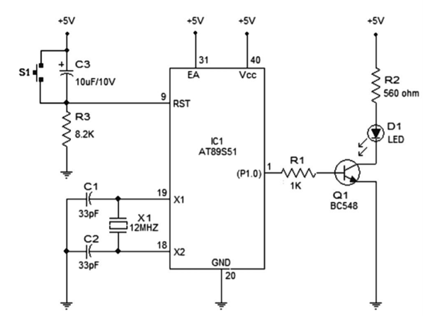
Figure 3. LED Interfacing
- In the circuit, push button switch S1, capacitor C3 and resistor R3 forms the reset circuitry.
- When S1 is pressed, voltage at the reset pin (pin9) goes high and this resets the chip. C1, C2 and X1 are related to the on -chip oscillator to produces the required clock frequency.
- P1.0 (pin1) is acts as the output pin. When P1.0turns high transistor Q1 is forward biased and LED gets ON. When P1.0 turns low, the transistor gets cut off and the LED extinguishes.
- The transistor driver circuit for the LED can be avoided and the LED can be connected directly to the P1.0 pinalong withthe series current limiting resistor(~1K).
- The time for which P1.0turns high and low (time period of the LED) is determined by the program.
Program:
START: CPL P1.0
ACALL WAIT
SJMP START
WAIT: MOV R4,#05H
WAIT1: MOV R3,#00H
WAIT2: MOV R2,#00H
WAIT3: DJNZ R2,WAIT3
DJNZ R3,WAIT2
DJNZ R4,WAIT1
RET
7-Segment Display Segments for all Numbers.

Fig.4: 7-Segment Display Segments for all Numbers
Then for a 7-segment display, we can produce a truth table giving the individual segments that need to be illuminated in order to produce the required decimal digit from 0 through 9 as shown below.
7-segment Display Truth Table
Decimal | Individual Segments Illuminated | ||||||
a | b | c | d | e | f | g | |
0 | × | × | × | × | × | × |
|
1 |
| × | × |
|
|
|
|
2 | × | × |
| × | × |
| × |
3 | × | × | × | × |
|
| × |
4 |
| × | × |
|
| × | × |
5 | × |
| × | × |
| × | × |
6 | × |
| × | × | × | × | × |
7 | × | × | × |
|
|
|
|
8 | × | × | × | × | × | × | × |
9 | × | × | × |
|
| × | × |
Driving a 7-segment Display
Although a 7-segment display can be thought of as a single display, it is still seven individual LEDs within a single package and as such these LEDs need protection from over current. LEDs produce light only when it is forward biased with the amount of light emitted being proportional to the forward current.
This means then that an LEDs light intensity increases in an approximately linear manner with an increasing current. So this forward current must be controlled and limited to a safe value by an external resistor to prevent damage to the LED segments.
The forward voltage drop across a red LED segment is very low at about 2-to-2.2 volts, (blue and white LEDs can be as high as 3.6 volts) so to illuminate correctly, the LED segments should be connected to a voltage source in excess of this forward voltage value with a series resistance used to limit the forward current to a desirable value.
Typically for a standard red coloured 7-segment display, each LED segment can draw about 15 mA to illuminated correctly, so on a 5 volt digital logic circuit, the value of the current limiting resistor would be about 200Ω (5v – 2v)/15mA, or 220Ω to the nearest higher preferred value.
So to understand how the segments of the display are connected to a 220Ω current limiting resistor consider the circuit below.
Driving a 7-segment Display
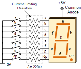
Fig.5: Driving a 7-segment Display
In this example, the segments of a common anode display are illuminated using the switches. If switch a is closed, current will flow through the “a” segment of the LED to the current limiting resistor connected to pin a and to 0 volts, making the circuit. Then only segment a will be illuminated. So a LOW condition (switch to ground) is required to activate the LED segments on this common anode display.
The most used ALPHANUMERIC displays are
1x16 (Single Line & 16 characters),
2x16 (Double Line & 16 character per line),
4x20 (four lines & Twenty characters per line).
The LCD requires 3 control lines that are RS, R/W & EN and 8- or 4-bit data lines.
The number of data lines depends on the mode of operation.
If operated in 8-bit mode then 8 data lines + 3 control lines that is 11 lines are required
And if operated in 4-bit mode then 4 data lines + 3 control lines that is 7 lines are required.
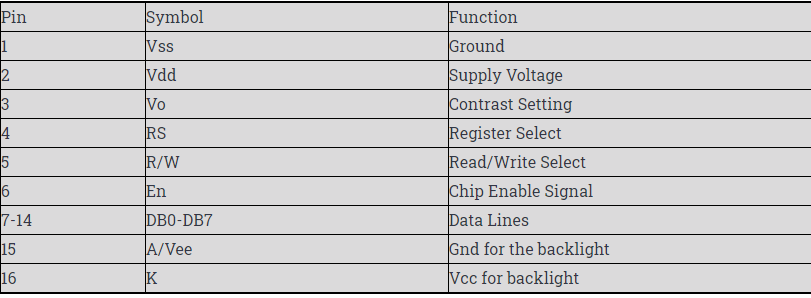
❖ When RS is low (0), the data is to be treated as a command.
❖ When RS is high (1), the data being sent is considered as text data which should be displayed on the screen.
❖ When R/W is low (0), the information on the data bus is being written to the LCD.
❖ When RW is high (1), the program is effectively reading from the LCD.
❖ The ENABLE pin is used to latch the data present on the data pins.
❖ A HIGH - LOW signal is required to latch the data.
❖ The LCD interprets and executes our command at the instant the EN line is brought low.
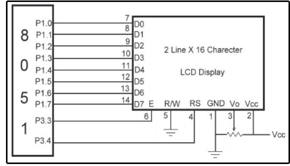
Figure 6. Interfacing of LCD with 8051.
To display a character on LCD we basically write into DDRAM. For a 2x16 LCD the DDRAM address for the first line is from 80h to 8fh & for the second line is 0c0h to 0cfh. So, to display 'H' on the 7th position of the first line then we can write at location 87h.
Data to be displayed

Command or Special Instruction

Write a program to display 'DNA TECHNOLOGY' on LCD.
ORG 0000h
CALL lcd_initialize
CALL lcd_clr
MOV A, #80h //Location from where Data is to be displayed
CALL lcd_command
MOV A, #'D'
CALL lcd_datadisplay
MOV A, #'N'
CALL lcd_datadisplay
MOV A, #'A'
CALL lcd_datadisplay
MOV A, #20h //Hex value for blank space to be displayed
CALL lcd_datadisplay
MOV A, #'T'
CALL lcd_datadisplay
MOV A, #'E'
CALL lcd_datadisplay
MOV A, #'C'
CALL lcd_datadisplay
MOV A, #'H'
CALL lcd_datadisplay
MOV A, #'N'
CALL lcd_datadisplay
MOV A, #'O'
CALL lcd_datadisplay
MOV A, #'L'
CALL lcd_datadisplay
MOV A, #'O'
CALL lcd_datadisplay
MOV A, #'G'
CALL lcd_datadisplay
MOV A, #'Y'
CALL lcd_datadisplay
Stop:
Ajmp stop.
ADC0808/0809:
ADC0808/0809 is a monolithic CMOS device which consists of 28 pins and gives 8-bit value in output for 8- channel ADC input pins (IN0-IN7).
It has a resolution of 8 therefore it can encode the analog data into one of the 256 levels (28).
It has three channel address lines namely: ADDA, ADDB and ADDC to select channels.
Pin Diagram for ADC0808
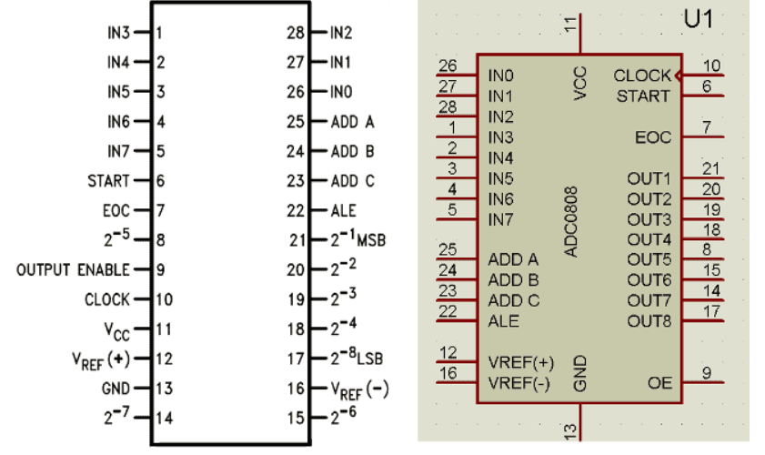
Figure 7. ADC 0808 Pin
ADC0808/0809 needs a clock pulse for conversion which can be provided by using an oscillator or microcontroller.
Select the input channel using address lines, like the input line IN0 by keeping all three address lines (ADDA, ADDB, ADDC) low.
Suppose IN2 is selected to keep ADDA and ADDB low and ADDC high.
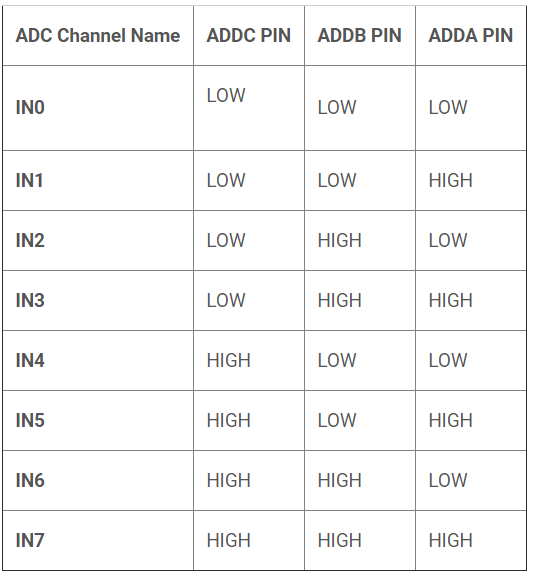
Figure 8. Channel selection
SOC [Start of conversion]:
When High to low signal is appears on the pin of ADC, and ADC starts conversion

Figure.9: SOC
EOC [End of conversion]:
To indicate completion of conversion ADC sends a high EOC signal to the microcontroller.
OE [Output Enable]:
When a high signal is applied to this pin, the output latch of ADC is enabled and the converted data is made available to the Microcontroller.
The reference voltage determines the range of analog input voltage.
For example: - If reference voltage is 5V then analog voltage ranges from 0V-5V. If the reference voltage is 2.56V then the range is from 0V-2.56V.
The frequency of the applied clock signal determines conversion speed.
Working:
⮚ Initially, microcontroller provides a 500 KHz clock signal to ADC0808 because the Timer 0 interrupt requires clock signal to operate to operate as ADC.
⮚ Then the microcontroller sends a LOW to HIGH level signal to ALE pin (active-high pin) of ADC0808 to enable the latch in the address.
⮚ By applying HIGH to LOW Level signal to SC (Start Conversion), ADC starts analog to digital conversion. And then wait for the EOC (End of Conversion) pin to go LOW.
⮚ When EOC goes LOW, it means analog to digital conversion has been completed and data is ready to use.
⮚ After this, the microcontroller enables the output line by applying a HIGH to LOW signal to the OE pin of ADC0808.
⮚ ADC0808 gives ratio metric conversion output at its output pins.
Radiometric conversion is given by
Vin/ (Vfs – Vz) = Dx / (Dmax – Dmin)
Where:
Vin is input voltage for conversion
Vfs is full scale voltage
Vz is zero voltage
Dx is data point being measured
Dmax is maximum data limit
Dmin is the minimum data limit.
Interfacing Diagram:
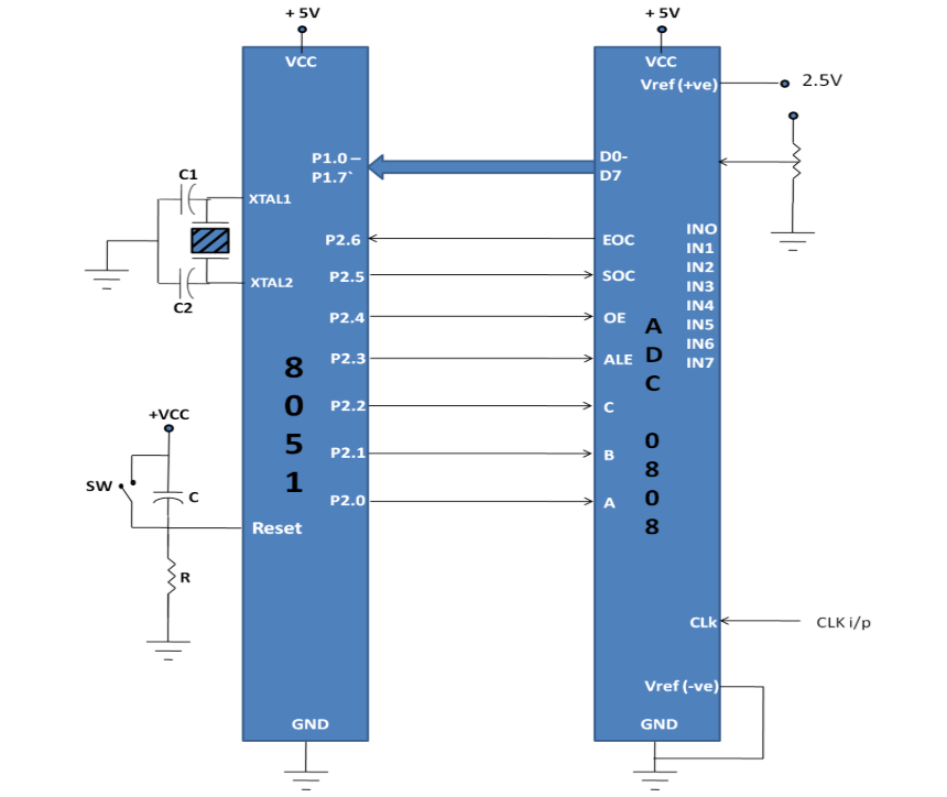
Figure 10. Interfacing 8051 with ADC0808
Program:
SOC EQU P2.6
EOC EQU P2.5
OE EQU P2.4
ALE EQU P2.3
ADDR_C EQU P2.2
ADDR_B EQU P2.1
ADDR_A EQU P2.0
ORG 0000H
MOV P1, #0FFH
SETB P2.5
CLR SOC
CLR OE
CLR ALE
AGAIN: CLR ADDR_C
CLR ADDR_B
CLR ADDR_A
SETB SOC
SET ALE
ACALL DELAY
CLR SOC
CLR ALE
BACK: JB EOC BACK
HERE: JNB EOC HERE
SETB OE
MOV A, P1
ACALL CONVERSION
ACALL DISPLAY
AGAIN: SJMP AGAIN
The (DAC) is a device used for converting digital pulses to analog signals.
There are two methods of converting digital signals to analog signals which are binary weighted method and R/2R ladder method.
The MC1408 (DAC0808) Digital to Analog Converter uses the R/2R ladder method. This method can achieve a higher degree of precision. DACs are judged by its resolution., If there are n digital input pins, there are 2n analog levels. So, 8 input DAC has 256 discrete voltage levels.
MC1408 DAC (or DAC0808)
In this chip the digital inputs are converted to current. The output current is known as Iout by connecting a resistor to the output to convert into voltage.
The total current provided by Iout pin is basically a function of binary numbers at the input pins D0 - D7 (D0 is the LSB and D7 is the MSB) of DAC0808 and the reference current Iref.
The following formula is showing the function of Iout
Iout=Iref⟮D7/2+D6/4+D5/8+D4/16+D3/32+D2/64+D1/128+D0/256⟯
The Iref is the input current. This must be provided into the pin 14. Generally, 2.0mA is used as Iref
Generating Sinewave using DAC and 8051 Microcontroller
For generating sinewave first, we need a look-up table to represent the magnitude of the sine value of angles between 0° to 360°. The sine function varies from -1 to +1.
In the table only integer values are applicable for DAC input. In this example we will consider 30° increments and calculate the values from degree to DAC input. We are assuming a full-scale voltage of 10V for DAC output.
We can follow this formula to get the voltage ranges.
Vout = 5V + (5 x sin θ)
The lookup table according to the angle and other parameters for DAC.
Angle (in θ) | Sinθ | Vout (Voltage Magnitude) | Values sent to DAC |
0 | 0 | 5 | 128 |
30 | 0.5 | 7.5 | 192 |
60 | 0.866 | 0.866 | 9.33 |
90 | 1.0 | 1.0 | 10 |
120 | 0.866 | 0.866 | 9.33 |
150 | 0.5 | 0.5 | 7.5 |
180 | 0 | 0 | 5 |
210 | -0.5 | -0.5 | 2.5 |
240 | -0.866 | -0.866 | 0.669 |
270 | -1.0 | -1.0 | 0 |
300 | -0.866 | -0.866 | 0.669 |
330 | -0.5 | -0.5 | 2.5 |
360 | 0 | 0 | 5 |
Circuit Diagram −
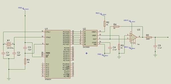
Fig.11: Interfacing
Source Code
#include <reg51.h>
Sfr DAC = 0x80; // Port P0 address
Void main()
{
Int sin value[12] = {128,192,238,255,238,192,128,64,17,0,17,64};
Int i;
While(1){
// infinite loop for LED blinking
For(i=0;i<12;i++)
{
DAC = sin_value[i];
}
}
}
Output
The output will look like this −
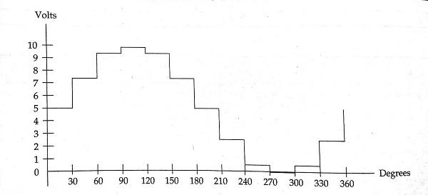
Fig.12: Output
Relays are mainly used for two basic operations.
One is a low voltage application. For low voltage applications preference is given to reduce the noise of the whole circuit.
Second, for high voltage applications, they are designed to reduce a phenomenon called arcing.
Interfacing
Here the transistor is wired as a switch for interfacing relay with 8051. This transistor drives the relay. The transistor will be in OFF state when the pin P3.0 is in the LOW state. When 1 is written to P3.0 current will flow to the base of the transistor and the relay energizes.
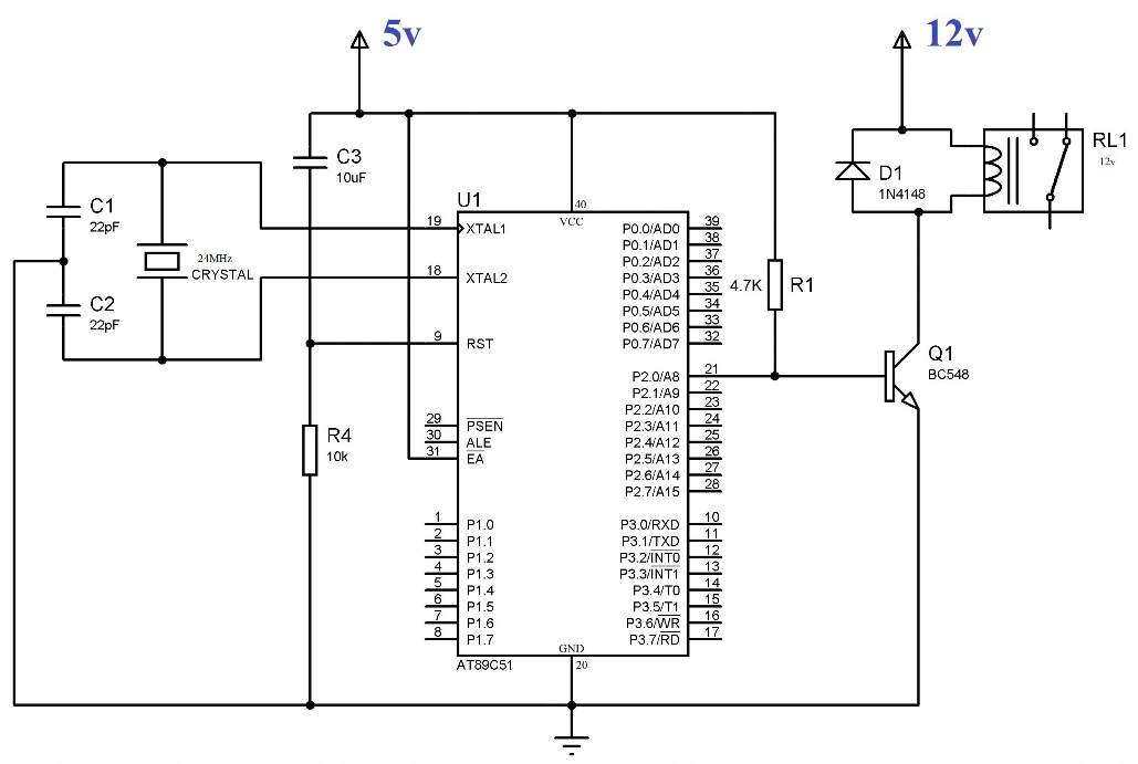
Figure 13. Interfacing with Relays.
Program:
Relay equ P0.0
Swequ P1.0
;*************************************************
Org 0000h
Main:clr relay ;Configure inp and outp
Setb sw
Up: jnbsw,on ;wait for switch to be pressed
Clr relay
Acall delay
Sjmp up
On: setb relay ;Turn ON relay
Acall delay
Acall delay
Here:jb sw,here ;wait for switch to be released
Clr relay ;Turn OFF relay
Acall delay
Acall delay
Sjmp up ;Loop
;*************************************************
Delay:mov r7,#0ffh ;delay subroutine
Again:mov r6,#0ffh
Djnz r6,$
Djnz r7,again
Ret
;*************************************************
End
References:
- Microprocessor Architecture, Programming, and ...Book by Ramesh S. Gaonkar
- 8085 Microprocessor: Programming and Interfacing Book by N. K. Srinath
- 8085 Microprocessors & Its Application Book by Nagoorkani
- C and the 8051: Building efficient applications Book by Thomas W. Schultz
- MICROCONTROLLER Book by V. Udayashankara