Unit - 2
Crystal Structure
Before analysing periodic patterns of atomic arrangements in crystals, we must first consider periodic patterns of point arrangements in space. This introduces the idea of a space lattice. A crystal structure can be represented using a space lattice as a framework.
A space lattice is a three-dimensional infinite array of points in which each point has the same surroundings as the others. Consider the two-dimensional square array of dots illustrated in Figure below for example, which is easy to express on paper.
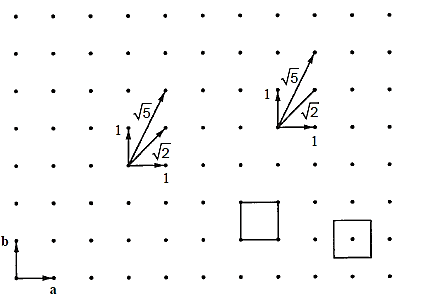
We can build the square array by repeatedly translating the two vectors a and b on the plane of the paper. The magnitudes of a and b are equivalent; hence unity can be assumed. The essential translation vectors that produce the square array are a and b, which have a 90° angle between them. We'll suppose that the array can be extended indefinitely to avoid end effects near the border.
The scenery is the same regardless of where we are in the array and looking out in a certain direction that lies on the plane of the paper. Consider a point in the arrays near surroundings. We can see another point at a distance of one unit if we look due north or due east from this place.
The nearest point along the northeast is  units away, whereas the nearest point along the north-northeast is
  units away. Because every point in the array fits the above specification, the array is referred to as a two-dimensional square lattice.
Key Takeaway:
A space lattice is a three-dimensional infinite array of points in which each point has the same surroundings as the others
Three noncoplanar vectors, a, b, and c, are translated repeatedly to form a three-dimensional space lattice. There are only 14 distinct ways of organising points in three-dimensional space in such a way that each arrangement conforms to the concept of a space lattice, it turns out. Bravais lattices are the 14 space lattices named after their discoverer. They are classified into seven crystal systems and are mentioned in Table by crystal system.
The cubic system is defined by three equal-magnitude mutually perpendicular translation vectors a, b, and c. The angle formed by b and c is α, the angle formed by c and an is β, and the angle formed by a and b is  . This angle notation is universal and should be followed consistently. The cubic crystal system has three space lattices, as indicated in Table: simple cubic, body centred cubic, and face centred cubic space lattices.
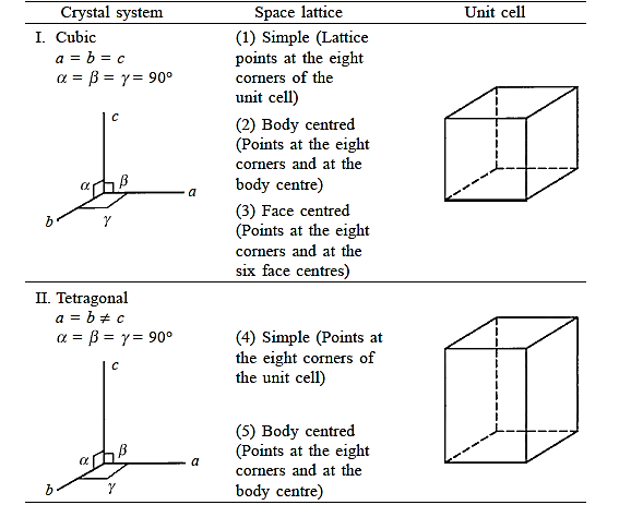
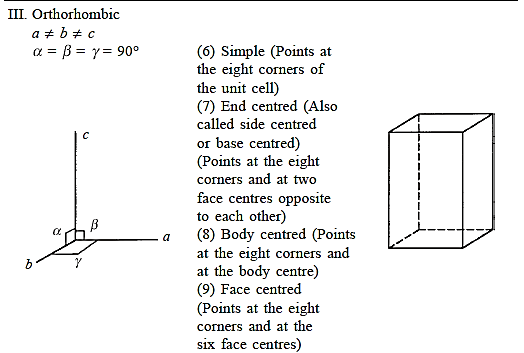
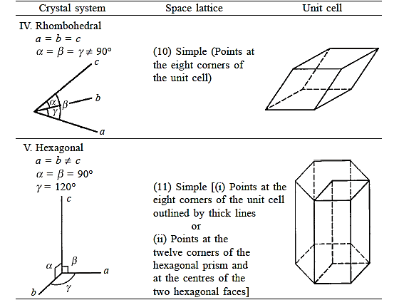
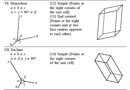
Crystals are symmetrical by nature. A cubic crystal has four-fold rotation symmetry along an axis that passes through the centres of two opposing sides of the unit cube. The crystal passes through identical points in space four times throughout each complete rotation around this axis. The symmetry elements of a crystal are rotational, translational, and reflection symmetry operations. Table shows the crystal systems in order of decreasing symmetry, with the cube being the most symmetric and the triclinic system being the least.
The tetragonal system is the next less symmetric crystal system after the cubic system. It is defined by three mutually perpendicular vectors, of which only two are of equal magnitude. Here, there are two space lattices.

There is no face-cantered tetragonal space lattice, which is interesting. As shown in Figure, any array of lattice points that can be represented by an FCT cell can also be described by a BCT cell. When there are two such alternatives of the same crystal system available to depict the same array of lattice points, the Bravais list is picked from the unit cell with the fewer lattice points.
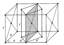
Three uneven but mutually perpendicular translation vectors define an orthorhombic cell. Four orthorhombic space lattices exist.

Key Takeaway:
Three noncoplanar vectors, a, b, and c, are translated repeatedly to form a three-dimensional space lattice. There are only 14 distinct ways of organising points in three-dimensional space in such a way that each arrangement conforms to the concept of a space lattice
Polymorphism is a phenomenon in which some metals and nonmetals have several crystal structures. Allotropy is a term used to describe a property seen in elemental solids. The crystal structure that prevails is influenced by both temperature and external pressure.
A space lattice is combined with a basis to generate a crystal structure.

The base of many elemental crystals is simple, consisting of one atom per lattice point. In such circumstances, the crystal is formed by simply placing one element's atom at each lattice point. Monoatomic crystals get their name from the fact that each lattice point has one atom as its base. This adjective is frequently left off. Unless otherwise stated, a BCC crystal is a monoatomic BCC crystal.
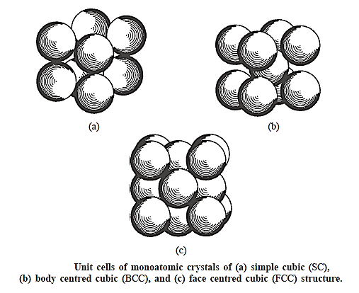
The atoms are represented as hard balls that are arranged in such a way that any two of their closest neighbour’s touch. The diameter of an atom in an elemental crystal is defined as the closest distance of approach between two atoms, which is consistent with the definition. This distance is the cube edge in the simple cubic unit cell. It is half of the body diagonal in the BCC cell. It is half of the face diagonal in the FCC cell. If the lattice parameter is a (cube edge),

Combining different bases and lattice parameters with the same space lattice can theoretically provide an unlimited number of crystal forms.
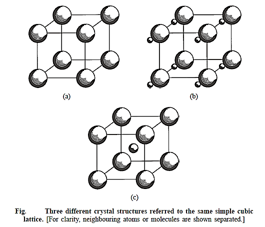
Three distinct bases are joined with a simple cubic lattice in Figure above. The crystal in Fig. a is monoatomic, containing only one atom at each lattice point. Neighbouring atoms are represented individually for clarity. A molecular crystal is depicted in Figure b, with a diatomic molecule at each lattice point. The larger atom in the molecule has its centre coincide with a lattice point, while the smaller atom does not. The number and types of atoms, the internuclear distance of separation between neighbours in the molecule, and the orientation of the molecule regarding the unit cell are all well defined in molecular crystals.
The cube's corner atoms are of one type in Fig. c, while the atom at the body centre is of a different type. The basis consists of two atoms, one positioned at a lattice point and the other half-way along the body diagonal, at the body centre, which is not a lattice point. The unit cell in the crystal can, of course, be adjusted so that the body centre becomes a lattice point and the body corners become non-lattice points. This crystal should not be mistaken with the monoatomic BCC crystal, which has the same type of atoms in both the body corner and the body centre.
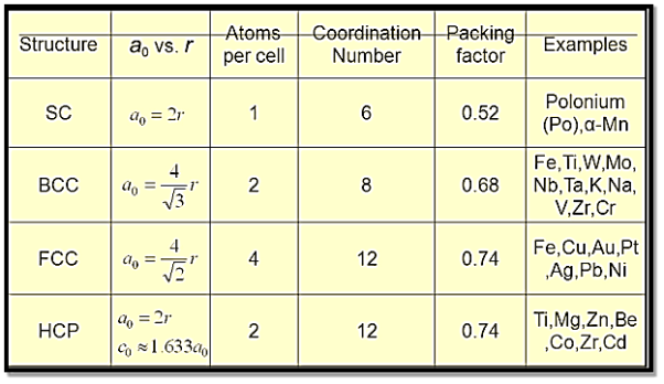
Because there are so many various crystal structures to choose from, it's sometimes easier to categorise them into categories based on unit cell configurations and/or atomic arrangements. The unit cell geometry, or the shape of the suitable unit cell parallelepiped without respect to the atomic positions in the cell, is one such system. Within this framework, a xyz coordinate system is formed with its origin at one of the unit cell corners; each of the three parallelepiped edges that extend from this corner coincides with one of the x, y, and z axes.
The six parameters that make up the unit cell geometry are the three edge lengths a, b, and c, as well as the three interaxial angles a, b, and g. These are shown in the diagram below and are commonly referred to as a crystal structure's lattice parameters.
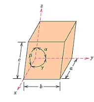
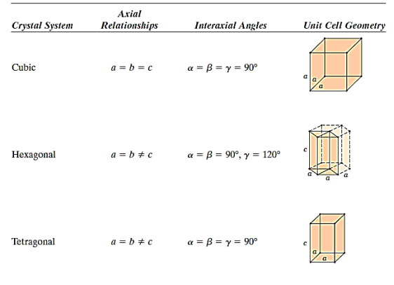
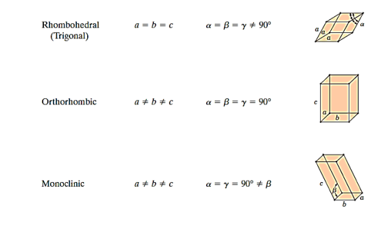
There are seven different conceivable combinations of a, b, and c, as well as a, b, and g, on this foundation, each of which represents a different crystal system. Cubic, tetragonal, hexagonal, orthorhombic, rhombohedral, 2 monoclinic, and triclinic are the seven crystal systems. The unit cell sketches and lattice parameter relationships for each are shown below.

Key Takeaway:
A space lattice is combined with a basis to generate a crystal structure.
The base of many elemental crystals is simple, consisting of one atom per lattice point. In such circumstances, the crystal is formed by simply placing one element's atom at each lattice point.
There are seven different conceivable combinations of a, b, and c, as well as a, b, and g, on this foundation, each of which represents a different crystal system. Cubic, tetragonal, hexagonal, orthorhombic, rhombohedral, 2 monoclinic, and triclinic are the seven crystal systems.
A unit cell can be used to describe a space lattice. The unit cell is the smallest unit that generates the space lattice when repeated in space indefinitely. The unit cell in the square lattice example above is the square formed by combining four adjacent lattice points, as shown in Figure. The effective number of lattice points in the unit cell is only one because every corner of this square is shared by four-unit cells that meet at that corner. The unit cell can also be viewed as a square with one lattice point in the middle and none at the corners.
Small groupings of atoms form a repeated pattern in crystalline materials, according to atomic order. As a result, it's common to divide crystal formations into little repetitive entities known as unit cells when discussing them. Most crystal formations have unit cells that are parallelepipeds or prisms with three sets of parallel faces, one of which is drawn within the aggregate of spheres.
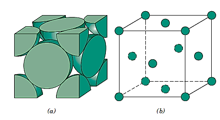
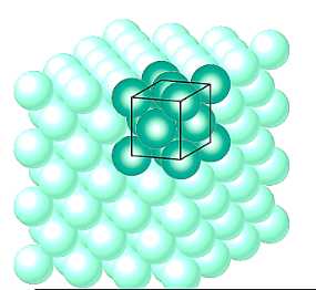
It happens to be a cube in this example. All of the atom positions in the crystal can be formed by translations of the unit cell integral lengths along each of its edges, hence a unit cell is chosen to symbolise the symmetry of the crystal structure. As a result, the unit cell is the basic structural unit or building block of the crystal structure, and its geometry and atom placements inside it define the crystal structure.
Parallelepiped corners are frequently aligned with the hard-sphere atoms' centres for practical reasons. Furthermore, for a given crystal structure, more than one unit cell may be used; nevertheless, we usually pick the unit cell with the highest amount of geometrical symmetry.
Key Takeaway:
The unit cell is the smallest unit that generates the space lattice when repeated in space indefinitely
This group of materials has metallic atomic bonding, which is nondirectional in nature. As a result, the number and location of closest-neighbour atoms are essentially unrestricted, resulting in relatively large numbers of nearest neighbours and dense atomic packings in most metallic crystal formations. In the case of metals, each sphere represents an ion core when utilising the hard-sphere model for the crystal structure.
The cubic crystal system is one of the most common (and by far the simplest) class of crystals. As the name itself suggests, all crystal structures of this system have a cube-shaped unit cell with edge length given by the lattice parameter ‘a’.
The three main common representatives are:
- Simple or Primitive Cubic (SC) (also known as primitive cubic)
- Body-centred Cubic (BCC)
- Face-centred Cubic (FCC)
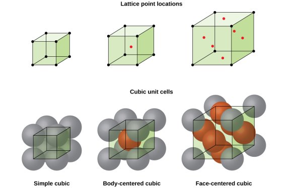
Simple or Primitive lattice
Number of atoms per unit cell:
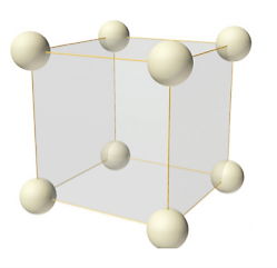
In simple or primitive lattice, 8 lattice points or 8 atoms are present at the 8 corners of the unit cell, each contributing 1/8thto the unit cell and hence there will be 8 x 1/8 = 1 lattice point per unit cell.
Coordination Number:
The number of nearest neighbour atoms or ions surrounding an atom or ion is known as coordination number. It is measure of closeness of packing of atoms in any given structure. It equals the number of nearest neighbours that surrounds each atom.
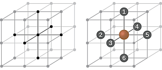
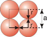
In simple cubic system 6 neighbours’ atoms at a distance of ‘a’ each from the selected atom as shown in figure. So, the coordination number of SC is six.
Atomic radius
Atoms are not hard spheres with distinct boundaries, so their sizes are not determined directly. However, the positions of the atoms in a solid can be determined by x-ray diffraction, and the sizes of the atoms are inferred from those distances. In this method, the radius of an atom is determined from the unit cell edge length (a), which is determined from the location of the atoms, and the assumption that the atoms touch.

Body-centred lattice
Number of atoms per unit cell:
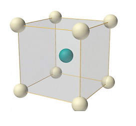
In body-centred lattice, in addition to the 8 atoms at 8 corners each contributing 1/8 th to the unit cell, there will be one complete atom at the centre of the unit cell. Therefore, number of atoms or lattice points in a body centred unit cell becomes 8 x 1/8 + 1 x 1 = 2.
Coordination Number:
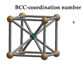
In Body Centred Cubic system 8 neighbour atoms are in touch with the selected atom as shown in figure. So, the coordination number of BCC is eight.
Atomic radius


Face-centred lattice (F)
Number of atoms per unit cell:
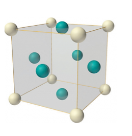
In case of face-centred lattice, in addition to the 8 atoms at 8 corners each contributing 1/8thto the unit cell, six atoms will be present at the centre of six faces of the cell each contributing 1/2nd to the unit cell. Therefore, number of atoms or lattice points in a face centred unit cell becomes 8 x 1/8 + 6 x 1/2 = 4.
Coordination Number:
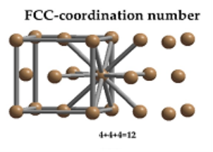
In Face Centred Cubic system 12 neighbour atoms are in touch with the selected atom as shown in figure. So, the coordination number of FCC is twelve.
Atomic radius
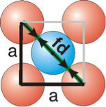


Relationship of Atomic Radii and Unit Cell Edge Lengths
Setting the edge length equal to 2r in the sc unit cell, and applying the Pythagorean theorem to the triangles shown in Figures we obtain the relationships between the atomic radius (r) of the atom and the edge length of the unit cell (a) given in Equation


Atomic packing factor
It is impossible to pack spheres without introducing some void space (space that is not occupied). How well the atoms pack a unit cell depends upon the unit cell type and is given by the packing efficiency of the unit cell. Solids with tightly packed unit cells are denser than those with low packing efficiencies. In this section, we examine the packing efficiencies of the cubic unit cells and show how to determine the density of a solid from its crystal structure.
Density
Density is the mass-to-volume ratio of a substance.

Packing Efficiency
Packing efficiency is the fraction of the unit cell that is occupied by particles. Spheres cannot be packed without creating some void space, but the amount of void space depends upon how well they are packed. Packing efficiency (PE) is that fraction of the unit cell volume that is actually occupied by particles, not void space. Thus, the packing efficiency of a unit cell is


a = the length of a side of the unit cell, so a3 is the volume of the unit cell.
r = the radius of the atoms that occupy the unit cell, so (4/3)πr3 is the volume of a single atom in the unit cell.
N = the number of atoms in the unit cell, so N(4/3)πr3 is the volume occupied by all of the atoms in the unit cell.
The unit cell size (a) is directly proportional to the atom size (r), so one can be defined in terms of the other.
Consequently, the packing efficiency depends only upon the cell type, not its size. As shown in the next sections, the relationship between a and r depends only upon the unit cell type.
Simple Cubes
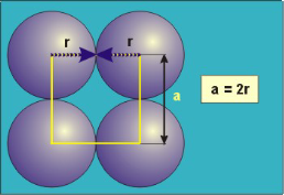
In the simple cubic unit cell, the spheres touch along the cell edge. Consequently, the edge length is two atomic radii
(a = 2r).
The properties of the simple cubic unit cell:
r = 0.5a
N = 1 atom/unit cell
Packing efficiency = 52%
Coordination number = 6
Body-Centred Cubes
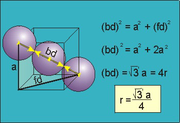
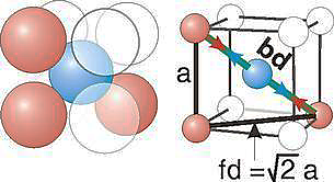
For the body-centered cubic unit cell, the spheres make contact along the body diagonal (bd), which is four atomic radii (each yellow arrow is one atomic radius), i.e., bd = 4r.
The body diagonal is related to the face diagonal (fd) and the cell edge (a) by the Pythagorean theorem. The relationship between the cell edge and the face diagonal was derived in the discussion of the fcc unit cell. The properties of the body-centered cubic unit cell:
r = 0.433 a
N = 2 atoms/unit cell
Packing efficiency = 68%
Coordination number = 8
Face-Centred Cubes
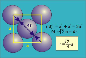
r= 0.354a
N = 4 atoms/unit cell
Packing efficiency = 74%
Coordination number = 12
As shown in the previous sections, the packing efficiency of a unit cell depends only on the cell type; it is independent of edge length and atomic radius because both cancel in the calculation. As might be expected, the packing efficiency increases as the number of atoms in the unit cell and the number of atoms that are packed around each atom (coordination number) increases.
Density of crystal
The first important thing to understand is that a cubic crystal is made up a crystal lattice or a space lattice structure. And as we have studied before, a space lattice is made up of a repeating arrangement of unit cells. A unit cell is the most basic structure of a crystalline solid.
Hence if we are able to find the density of a unit cell, it can be said that we have found the density of the cubic crystal itself. With this in mind, let us determine how to arrive at the density of a cubic crystal cell.
Now as we know a unit cell also has a cubic structure. It has one, two or four atoms located at various lattice points. Now with the help of geometry, some basic calculations and certain attributes of this cubic structure we can find the density of a unit cell. Let us start with the basic formula for the density of any solid. This formula is
Density = Mass/ Volume
The density of a Unit Cell will be
D = Mass of Unit Cell / Volume of Unit Cell
Mass of a Unit Cell
Now to calculate the mass of one unit cell we add up the mass of all the atoms contained in that particular cell. The number of atoms will depend on the kind of cell it is. So to obtain the mass of a unit cell we multiply the number of atoms “n” into the mass of each atom” m”.
Mass of Unit Cell = m × n
But now the question remains, what is the mass of an atom? Well, this can be represented in terms of its Avogadro Number (NA)., i.e. number of units in one mole of any substance and the molar mass of an atom. So the mass of an atom can be calculated as
Mass of an Atom = 
Mass of an Atom = 
So now the formula for Mass of Unit Cell is as follows
Mass of Unit Cell = n × 
Volume of Unit Cell
As we already know, the unit cell is a cubic structure. So the Volume of a cube is the cube of the length of the side, Assume that the length of the side of the cube is “a”.
Volume of Unit Cell = a3
Density of Unit Cell
And now we finally arrive at the actual formula for the density of a unit cell
Density of a Unit Cell = 
Density of a Unit Cell = 
The Hexagonal Close-Packed Crystal Structure:
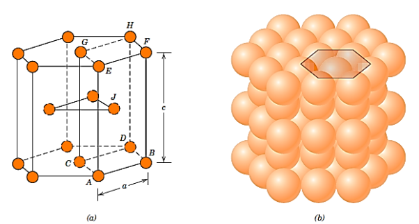
Not all metals have cubic symmetry unit cells; the final typical metallic crystal structure to be addressed has a hexagonal unit cell. Figure 1 illustrates a reduced sphere unit cell for this structure, which is referred to as hexagonal close-packed (HCP); Figure 2 shows an assemblage of many HCP unit cells. Six atoms create regular hexagons on the top and bottom faces of the unit cell, which encircle a single atom in the centre.
Between the top and bottom planes is another plane that supplies three more atoms to the unit cell. The atoms in this midplane have atoms in next two planes as nearest neighbours. Each unit cell contains the equivalent of six atoms: one-sixth of each of the 12 top and bottom face corner atoms, half of each of the two centre face atoms, and all three midplane inside atoms.
If a and c represent, respectively, the short and long unit cell dimension

However, for some HCP this ratio deviates from ideal value.
The coordination number and the atomic packing factor for the HCP crystal structure are the same as for FCC.
Key Takeaway:
Point Coordinates:
Any point within a unit cell can be described by its coordinates expressed as fractional multiples of the unit cell edge lengths (i.e., in terms of a, b, and c). Consider the unit cell and the point P that is located within it, as illustrated in Figure. P's position is specified using the generalised coordinates q, r, and s, where q is a fractional length of an along the x axis, r is a fractional length of b along the y axis, and s is the same.
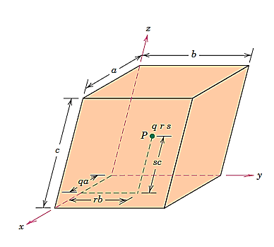
As a result, the coordinates q r s with values less than or equal to unity are used to designate P's position. Furthermore, we have chosen not to use commas or any other punctuation marks to separate these coordinates (which is the normal convention).
Crystallographic directions:
A crystallographic direction is a line or vector connecting two points. The three directional indices are calculated using the steps below:
- A convenient-length vector is positioned so that it passes through the coordinate system's origin. If parallelism is maintained, any vector can be translated without change throughout the crystal lattice.
- Determine the length of each of the three axis' vector projections, which are measured in terms of the unit cell dimensions a, b, and c.
- To reduce these three numbers to the smallest integer values, they are multiplied or divided by a common factor.
- The three indices, not separated by commas, are enclosed in square brackets, thus: [uvw]. The u, v, and w integers correspond to the reduced projections along the x, y, and z axes, respectively.
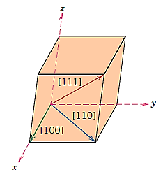
Positive and negative coordinates will exist for each of the three axes. Negative indices, which are represented by a bar over the appropriate index, are also possible.
Example:

Would have a component in the -y direction. Also, changing the signs of all indices produces an antiparallel direction

If more than one direction (or plane) is to be specified for a particular crystal structure, it is imperative for the maintaining of consistency that a positive–negative convention, once established, not be changed.
Several nonparallel paths with different indices are crystallographic ally comparable for crystal structures; this means that the spacing of atoms along each direction is the same. For example, in cubic crystals, all the directions represented by the following indices are equivalent:  and
and  As a convenience, equivalent directions are grouped together into a family, which are enclosed in angle brackets, thus:
  Furthermore, directions in cubic crystals having the same indices without regard to order or sign—for example,
  are equivalent. This is, in general, not true for other crystal systems. For example, for crystals of tetragonal symmetry,
  directions are equivalent, whereas
 are not.
Hexagonal Crystals:
For hexagonal symmetry crystals, an issue occurs in that some crystallographic equivalent orientations do not have the same set of indices. A four-axis, or Miller–Bravais, coordinate system is used to get around this.
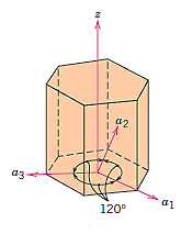
Conversion from the three-index system to the four-index system,


Primed indices are related with the three-index system, while unprimed indices are associated with the new Miller–Bravais four-index system.
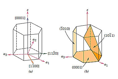
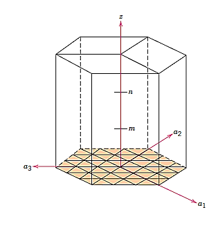
Crystallographic directions charting for hexagonal crystals is more difficult than for crystals from the other six systems. The four-axis coordinate system presented in Figure is sometimes more practical for hexagonal. On the basal plane, a grid consisting of sets of lines parallel to each of the a1, a2, and a3 axes has been built. Within the hexagonal unit cell, the intersections of two sets of parallel lines (e.g., those for a2, and a3) lie on and trisect the other axis (e.g., divide a1 into thirds).
Furthermore, Figure's z axis is divided into three equal lengths (at trisection points m and n). This approach will be referred to as a reduced-scale coordinate system. An approach similar to that described earlier (which includes vector projections along relevant axes) is used to construct a direction given by four indices.
Crystallographic planes:
A crystal structure's plane orientations are represented in a similar way. The unit cell serves as the foundation once more, with the three-axis coordinate system depicted in Figure. Crystallographic planes are defined by three Miller indices in all but the hexagonal crystal system (hkl). Any two planes that are parallel to each other have the same indices and are equivalent. The following is the technique for calculating the h, k, and l index numbers:
- If the plane passes through the chosen origin, either a new parallel plane must be built within the unit cell by proper translation, or a new origin must be formed at the corner of another unit cell.
- The crystallographic plane intersects or parallels each of the three axes at this location, and the length of the planar intercept for each axis is given by the lattice parameters a, b, and c.
- These numbers' reciprocals are calculated. A plane parallel to an axis may be thought to have an infinite intercept and so a zero index.
- If necessary, multiply or divide these three values by a common factor to get the set of lowest integers. 3
- Finally, the integer indices are placed between parenthesis if they are not separated by commas, as follows: (hkl).
A bar or minus sign over the corresponding index indicates an intercept on the negative side of the origin. Reversing the directions of all indices also creates a plane that is parallel to, on the opposite side of, and equidistant from the origin. Figure depicts a number of low-index planes.
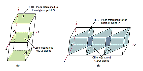
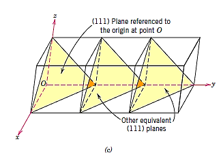
The fact that planes and directions with the same indices are perpendicular to one another is an important and unique feature of cubic crystals; however, there are no clear geometrical correlations between planes and directions with the same indices in other crystal systems.
Key Takeaway:
Positive and negative coordinates will exist for each of the three axes
Several nonparallel paths with different indices are crystallographic ally comparable for crystal structures;
For hexagonal symmetry crystals, an issue occurs in that some crystallographic equivalent orientations do not have the same set of indices


Crystallographic planes are defined by three Miller indices in all but the hexagonal crystal system (hkl).
Defects can be found in any solid material. Defects are categorised based on their geometry for ease of characterisation, which is reasonable given that defects are damaged regions in a solid's volume. Defects include:
- Point defects (zero-dimensional)
- Line defects (single dimensional)
- Surface defects (two dimensional)
- Volume defects (three dimensional)
Point defects are defective point-like spots in the crystal, as the name implies. A point flaw is typically 1-2 atomic diameters in size.
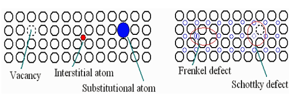
A vacancy is a void in the lattice where an atom is missing. It is commonly made when the liquid is cooled to become a solid. Other methods of creating vacancies exist, however they also occur naturally because of thermal excitation and are thermodynamically stable at temperatures above zero. At a certain temperature (T), the fraction of lattice sites that are unoccupied is at equilibrium.

Where n is the number of unoccupied sites in N lattice locations, k denotes the gas constant, T denotes the absolute temperature in kelvins, and Q denotes the energy necessary to transfer an atom from the interior to the surface of a crystal. The equation clearly shows that the number of vacancies increases exponentially with temperature. When the density of vacancies is high enough, they can cluster together and produce voids.
An atom that occupies a position outside of the typical lattice position is known as an interstitial atom or interstitially. It could be a foreign impurity atom or the same sort of atom as the rest of the surrounding atoms (self-interstitial). If the atomic packing factor is low, interstitially is most likely.
Substitution is another method for fitting an impurity atom into a crystal lattice. A substitutional atom is a foreign atom that displaces the parent atom from its native lattice position.
There is a change in the coordination of atoms around vacancies and foreign atoms (both interstitial and substitutional) in the event of vacancies and foreign atoms (both interstitial and substitutional). This implies the forces aren't balanced the same way they are for other atoms in the solid, resulting in lattice deformation around the defect.
The occurrence of point defects in ionic crystals is constrained by the charge neutrality criterion. In ionic solids, there are two types of point defects.
- The Frenkel defect occurs when an ion is moved from a regular position to an interstitial position, causing a vacancy. Because cations are smaller than anions, they can be easily displaced. Because more energy is required to drive the atoms into the interstitial sites, closed packed formations have fewer interstitials and displaced ions than voids.
- When the valency of the ions is equal, a pair of one cation and one anion can be missing from an ionic crystal without violating the charge neutrality criterion. Schottky defect refers to the resulting pair of unoccupied sites. Alkali halides have a lot of this type of point defect. Like single vacancies, these ion-pair vacancies aid atomic diffusion.
Key Takeaway:

The Frenkel defect occurs when an ion is moved from a regular position to an interstitial position
Schottky defect refers to the resulting pair of unoccupied sites
Dislocations are sometimes known as line flaws (one-dimensional faults). They occur when the usual arrangement of atoms along a line (dislocation line) in a solid abruptly changes. They are found in high densities and have a significant impact on the material's mechanical properties. They are distinguished by the Burgers vector (b), whose size and direction may be measured by creating a loop around the disrupted region and observing the extra inter-atomic separation required to finish the loop. In metals, the Burgers vector points in the direction of a densely packed lattice. It's only found in a dislocation.
When an extra incomplete plane is added, dislocations occur. The plane's dislocation line is near the very end. The best way to understand dislocations is to consider two limiting cases: edge dislocation and screw dislocation.
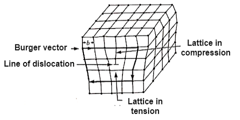
Causes of line imperfections are:
- Thermal stresses or external stresses causing plastic flow.
- Crystal growth.
- Phase transformation.
- Segregation of solute atoms causing mismatches.
Types of line imperfections:
- Edge line imperfection or dislocation:
It is formed by adding extra partial planes of atoms.
b. Screw line imperfection or dislocation:
A screw dislocation has its displacement or Burger Vector parallel to the linear defect but there is a distortion of the plane.
These dislocations are responsible for the useful property of ductility in metal, ceramics and polymers.
Key Takeaway:
Dislocations are sometimes known as line flaws (one-dimensional faults). They occur when the usual arrangement of atoms along a line (dislocation line) in a solid abruptly changes
Dislocations are linear defects; they are lines through the crystal along which crystallographic registry is lost. Their principal role in the microstructure is to control the yield strength and subsequent plastic deformation of crystalline solids at ordinary temperatures. Dislocations also participate in the growth of crystals and in the structures of interfaces between crystals. They act as electrical defects in optical materials and semiconductors, in which they are almost always undesirable. Dislocations influence many aspects of physical behaviour; they are studied almost exclusively in Materials Science.
The low observed values of the critical shear stress are explained in terms of the motion through the lattice of a line imperfection known as a dislocation. The concept of dislocations was introduced by Prandtl and Dehlinger.
Dislocations are linear defects that commonly form in metals as a result of the application of stresses due to repeated bending. They play an important role in both the strength and the
Failure of materials: work hardening (such as beating a red-hot piece of metal on an anvil) has been used for centuries by blacksmiths to introduce dislocations into materials, increasing their yield strengths. On the other hand, the infamous metal fatigue fracture are initiated by dislocations, which eventually form persistent slip bands that nucleate short cracks
Two main types of dislocations are identified: edge dislocations and screw dislocations, although most real dislocation are intermediate between these types. They are characterised by two direction vectors: the dislocation direction—the direction of the linear structure in question, and the Burgers vector —the principal direction of the strain (displacement) field near the dislocation.
Screw dislocation
A screw dislocation marks the boundary between slipped and unslipped parts of the crystal. The boundary parallels the slip direction, instead of lying perpendicular to it as for the edge dislocation. The screw dislocation may be thought of as produced by cutting the crystal partway through with a knife and shearing it parallel to the edge of the cut by one atom spacing.
A screw dislocation transforms successive atom planes into the surface of a helix: this accounts for the name of the dislocation.
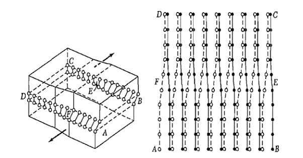
Figure: A screw dislocation - A part ABEF of the slip plane has slipped in the direction parallel to the dislocation line EF A screw dislocation may be visualized as a helical arrangement of lattice planes, such that we change planes on going completely around the dislocation line.
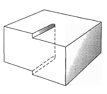
Figure: Another view of a screw dislocation. The broken vertical line that marks the dislocation is surrounded by strained material.
Edge dislocation
Figure shows a simple cubic crystal in which slip of one atom distance has occurred over the left half of the slip plane but not over the right half. The boundary between the slipped and unslipped regions is called the dislocation.
Its position is marked by the termination of an extra vertical half-plane of atoms crowded into the upper half of the crystal as shown in Figure 35. Near the dislocation the crystal is highly strained. The simple edge dislocation extends indefinitely in the slip plane in a direction normal to the slip direction
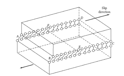
Figure: An edge dislocation EF in the glide plane ABCD. The figure shows the slipped region ABEF in which the atoms have been displaced by more than half a lattice constant and the unslipped region FECD with displacement less than half a lattice constant.
The motion of an edge dislocation through a crystal is analogous to the passage of a ruck or wrinkle across a rug: the ruck moves more easily than the whole rug. If atoms on one side of the slip plane are moved with respect to those on the other side, atoms at the slip plane will experience repulsive force from some neighbours and attractive forces from others across the slip plane.
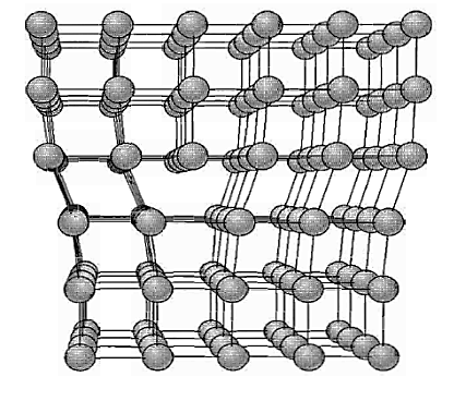
Figure: Structure of an edge dislocation. The deformation may be thought of as caused by inserting an extra plane of atoms on the upper half of the axis. Atoms in the upper half-crystal are compressed by the insertion; those in the lower half are extended
These forces cancel to a first approximation. The external stress required to move a dislocation has been calculated and is quite small, below l05 dyn/cm2 when the bonding forces in the crystal are not highly directional. Thus dislocations may make a crystal very plastic. Passage of a dislocation through a crystal is equivalent to a slip displacement of one part of the crystal.
Burger’s vector
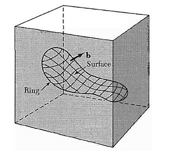
Other dislocation forms may be constructed from segments of edge and screw dislocations. Burgers has shown that the most general form of a linear dislocation pattern in a crystal can be described as shown in Figure.
We consider any closed curve within a crystal, or an open curve terminating oil the surface at both ends:
(a) Make a cut along any simple surface bounded by the line.
(b) Displace the material on one side of this surface by a vector b relative to the other side; here b is called the Burgers vector.
(c) In regions where b is not parallel to the cut surface, this relative displacement will either produce a gap or cause the two halves to overlap. In these cases we imagine that we either add material to fill the gap or subtract material to prevent overlap.
(d) Re-join the material on both sides. We leave the strain displacement intact at the time of rewelding, but afterwards we allow the medium to come to internal equilibrium. The resulting strain pattern is that of the dislocation characterized jointly by the boundary curve and the Burgers vector. The Burgers vector must be equal to a lattice vector in order that the rewelding process will maintain the crystallinity of the material.
General method of forming a dislocation ring in a medium. The medium is represented by the rectangular block. The ring is represented by the closed curve in the interior in the block. A cut is made along the surface bounded by the curve and indicated by the contoured area. The material on one side of the cut is displaced relative to that on the other by vector distance b, which may be oriented arbitrarily relative to the surface. Forces will be required to effect the displacement. The medium is filled in or cut away so as to be continuous after the displacement. It is then joined in the displaced state and the applied forces are relaxed. Here b is the Burgers vector of the dislocation.
The Burgers vector of a screw dislocation (Figures. 33 and 34) is parallel to the dislocation line; that of an edge dislocation (Figures. 35 and 36) is perpendicular to the dislocation line and lies in the slip plane.
Key Takeaway:
- Dislocations are linear defects; they are lines through the crystal along which crystallographic registry is lost.
- The low observed values of the critical shear stress are explained in terms of the motion through the lattice of a line imperfection known as a dislocation.
- Dislocations are linear defects that commonly form in metals as a result of the application of stresses due to repeated bending.
- Two main types of dislocations are identified: edge dislocations and screw dislocations, although most real dislocation are intermediate between these types.
- They are characterised by two direction vectors: the dislocation direction—the direction of the linear structure in question, and the Burgers vector —the principal direction of the strain (displacement) field near the dislocation.
References:
- Material Science and Engineering by V. Raghavan
- Material Science and Engineering by William D. Callister
- Material Science by Prof. Satish V. Kailas (Associate Professor, Dept. Of Mechanical Engineering, Indian Institute of Science, Bangalore – 560012) NPTEL