UNIT 5
SOLID STATE PHYSICS AND SEMICONDUCTOR PHYSICS
Bands are formed by the closely spaced orbitals.
There are three types of bands:
1. Valance Bands: Valence band it is a group of orbitals which contain electrons in the shell. Or we can say It is also defined as the energy band that comprises of valence electrons present in the outermost shell of an atomic structure.
These valence electrons, when provided with sufficient energy, get changed into free electrons and moves to conduction band thereby causing conductivity. It is at a lower energy level than the conduction band in the energy level diagram.
2. Conduction Band: Conduction band is a group of empty orbitals of the shells that do not contain any electron due to their configuration making the orbitals of higher energy levels.
When the electrons pass from valance band to the conduction band these solids conduct electricity with flow of charges in the form of electrons.
3. Forbidden Energy Band: These two bands are separated by a certain amount of energy known as the forbidden energy gap. In this band not a single electron is available. It diagram it is named as Band Gap.
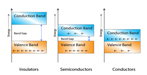
Let us distinguish between conductor, semiconductors and insulator on the basis of these bands.
1 Figure: |
- In Conductors: The valance band and the conduction band overlap each other. This makes it easy for the electricity to pass through them. In conductors, the valence band is either not fully occupied with electrons, or the filled valence band overlaps with the empty conduction band. In general, both states occur at the same time, the electrons can therefore move inside the partially filled valence band or inside the two overlapping bands. In conductors there is no band gap between the valence band and conduction band.
- In Semi-conductors: there is a slight gap between the conduction band and the valance band. This band gap is less than or equal to 1.4 eV. The electrons from valance shell take a little energy to excite from valance band to the conduction band. Even in semiconductors, there is a band gap, but compared to insulators it is so small that even at room temperature electrons from the valence band can be lifted into the conduction band. The electrons can move freely and act as charge carriers.
- In Insulators: In insulators the valence band is fully occupied with electrons due to the covalent bonds. To achieve conductivity, electrons from the valence band have to move into the conduction band. the energy gap is considerably large and the electrons of the valance band cannot be excited to the conduction band before the melting or the dissociation of the solid. This means that under the practically ambient condition it cannot conduct electricity.
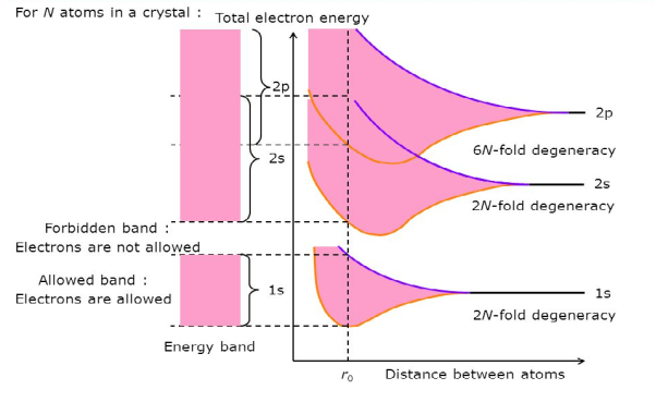
Consider an isolated silicon atom; its energy levels are quantized. When two identical atoms are brought closer together, the quantized energy levels hybridize and split into two different levels because of the mutual interaction of the two atoms. More generally, when N atoms are moved closer, until they reach the equilibrium inter-atomic distance d, the energy levels split into N levels. These N levels are very close to each other if N is large (which is the case in a crystal) so that they eventually form a continuous energy band.
2 Figure: Formation of Energy band as a function of interatomic distance (distance between atoms) |
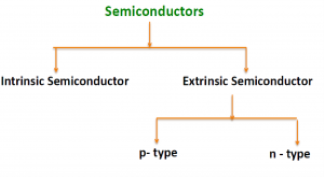
There are two basic groups or classifications that can be used to define the different semiconductor types:
- Intrinsic Semiconductor
- Extrinsic Semiconductor
|
The semiconductor is divided into two types. One is Intrinsic Semiconductor and other is an Extrinsic semiconductor. The pure form of the semiconductor is known as the intrinsic semiconductor and the semiconductor in which intentionally impurities is added for making it conductive is known as the extrinsic semiconductor.
The conductivity of the intrinsic semiconductor become zero at room temperature while the extrinsic semiconductor is very little conductive at room temperature. The detailed explanation of the two types of the semiconductor is given below.
INTRINSIC SEMICONDUCTOR
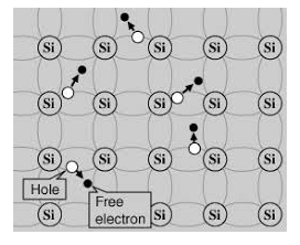
An intrinsic type of semiconductor material made to be very pure chemically. As a result it possesses a very low conductivity level having very few number of charge carriers, namely holes and electrons, which it possesses in equal quantities.
3 Figure: |
The most commonly used semiconductor basics material by far is silicon. Silicon has four valence electrons in its outermost shell which it shares with its neighbouring silicon atoms to form full orbital’s of eight electrons. The structure of the bond between the two silicon atoms is such that each atom shares one electron with its neighbour making the bond very stable.
As there are very few free electrons available to move around the silicon crystal, crystals of pure silicon (or germanium) are therefore good insulators. Silicon atoms are arranged in a definite symmetrical pattern making them a crystalline solid structure. A crystal of pure silica (silicon dioxide or glass) is generally said to be an intrinsic crystal (it has no impurities) and therefore has no free electrons.
An extremely pure semiconductor is called as Intrinsic Semiconductor. On the basis of the energy band phenomenon, an intrinsic semiconductor at absolute zero temperature is shown below.
4 Figure: |
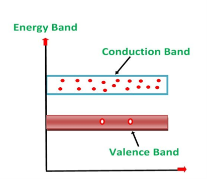
Its valence band is completely filled and the conduction band is completely empty. When the temperature is raised and some heat energy is supplied to it, some of the valence electrons are lifted to conduction band leaving behind holes in the valence band as shown below.
5 Figure: |
A hole is the absence of an electron in a particular place in an atom. Although it is not a physical particle in the same sense as an electron, a hole can be passed from atom to atom in a semiconductor material. It is considered to have positive charge. Holes are positive charge carriers.
The electrons reaching at the conduction band move randomly. The holes created in the crystal also free to move anywhere.
This behaviour of the semiconductor shows that they have a negative temperature coefficient of resistance. This means that with the increase in temperature, the resistivity of the material decreases and the conductivity increases.
But simply connecting a silicon crystal to a battery supply is not enough to extract an electric current from it. To do that we need to create a “positive” and a “negative” pole within the silicon allowing electrons and therefore electric current to flow out of the silicon. These poles are created by doping the silicon with certain impurities.
DOPING
The process by which an impurity is added to a semiconductor is known as Doping. The amount and type of impurity which is to be added to a material has to be closely controlled during the preparation of extrinsic semiconductor. Generally, one impurity atom is added to a 108 atoms of a semiconductor.
The purpose of adding impurity in the semiconductor crystal is to increase the number of free electrons or holes to make it conductive.
If a Pentavalent impurity, having five valence electrons is added to a pure semiconductor a large number of free electrons will exist. Which make a n-type extrinsic semiconductor.
If a trivalent impurity having three valence electrons is added, a large number of holes will exist in the semiconductor. Which make a p-type extrinsic semiconductor.
EXTRINSIC SEMICONDUCTOR
Extrinsic types of semiconductor are those where a small amount of impurity has been added to the basic intrinsic material. This 'doping' uses an element from a different periodic table group and in this way it will either have more or less electrons in the valence band than the semiconductor itself. This creates either an excess or shortage of electrons. In this way two types of semiconductor are available: Electrons are negatively charged carriers. Holes are positively charged carriers.
Depending upon the type of impurity added the extrinsic semiconductor may be classified as n type semiconductor and p type semiconductor.
P-TYPE EXTRINSIC SEMICONDUCTOR
The extrinsic p-Type Semiconductor is formed when a trivalent impurity is added to a pure semiconductor in a small amount, and as a result, a large number of holes are created in it. A large number of holes are provided in the semiconductor material by the addition of trivalent impurities like Gallium and Indium. Such type of impurities which produces p-type semiconductor are known as an Acceptor Impurities because each atom of them create one hole which can accept one electron.
In a P-type semiconductor material there is a shortage of electrons, i.e. there are 'holes' in the crystal lattice. Electrons may move from one empty position to another and in this case it can be considered that the holes are moving. This can happen under the influence of a potential difference and the holes can be seen to flow in one direction resulting in an electric current flow. It is actually harder for holes to move than for free electrons to move and therefore the mobility of holes is less than that of free electrons. Holes are positively charged carriers.
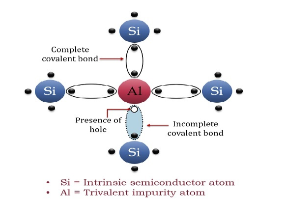
A trivalent impurity like Aluminium, having three valence electrons is added to Silicon crystal in a small amount. Each atom of the impurity fits in the Silicon crystal in such a way that its three valence electrons form covalent bonds with the three surrounding Silicon atoms as shown in the figure below.
6 Figure: |
ENERGY BAND DIAGRAM OF P-TYPE SEMICONDUCTOR
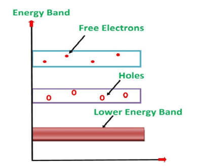
The energy band diagram of a p-Type Semiconductor is shown below.
7 Figure |
A large number of holes or vacant space in the covalent bond is created in the crystal with the addition of the trivalent impurity. A small or minute quantity of free electrons is also available in the conduction band.
They are produced when thermal energy at room temperature is imparted to the Silicon crystal forming electron-hole pairs. But the holes are more in number as compared to the electrons in the conduction band. It is because of the predominance of holes over electrons that the material is called as a p-type semiconductor. The word “p” stands for the positive material.
CONDUCTION THROUGH P TYPE SEMICONDUCTOR
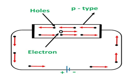
In p type semiconductor large number of holes are created by the trivalent impurity. When a potential difference is applied across this type of semiconductors.
8 Figure: |
The holes are available in the valence band are directed towards the negative terminal. As the current flow through the crystal is by holes, which are carrier of positive charge, therefore, this type of conductivity is known as positive or p type conductivity. In a p type conductivity the valence electrons move from one covalent to another.
The conductivity of n type semiconductor is nearly double to that of p type semiconductor. The electrons available in the conduction band of the n type semiconductor are much more movable than holes available in the valence band in a p type semiconductor. The mobility of holes is poor as they are more bound to the nucleus.
Even at the room temperature the electron hole pairs are formed. These free electrons which are available in minute quantity also carry a little amount of current in the p type semiconductors.
N-TYPE EXTRINSIC SEMICONDUCTOR
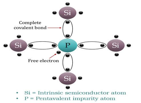
When a few Pentavalent impurities such as Phosphorus whose atomic number is 15, which is categorised as 2, 8 and 5. It has five valence electrons, which is added to silicon crystal. Each atom of the impurity fits in four silicon atoms as shown in the figure below.
Hence, each Arsenic atom provides one free electron in the Silicon crystal. Since an extremely small amount of Phosphorus, impurity has a large number of atoms; it provides millions of free electrons for conduction.
9 Figure: |
An N-type semiconductor material has an excess of electrons. In this way, free electrons are available within the lattices and their overall movement in one direction under the influence of a potential difference results in an electric current flow. This in an N-type semiconductor, the charge carriers are electrons.
ENERGY DIAGRAM OF N-TYPE SEMICONDUCTOR
A large number of free electrons are available in the conduction band because of the addition of the Pentavalent impurity. These electrons are free electrons which did not fit in the covalent bonds of the crystal. However, a minute quantity of free electrons is available in the conduction band forming hole- electron pairs.
The Energy diagram of the n-type semiconductor is shown in the figure below.
10 Figure: |
- The addition of pentavalent impurity results in a large number of free electrons.
- When thermal energy at room temperature is imparted to the semiconductor, a hole-electron pair is generated and as a result, a minute quantity of free electrons is available. These electrons leave behind holes in the valence band.
- Here n stands for negative material as the number of free electrons provided by the pentavalent impurity is greater than the number of holes.
CONDUCTION THROUGH N-TYPE SEMICONDUCTOR
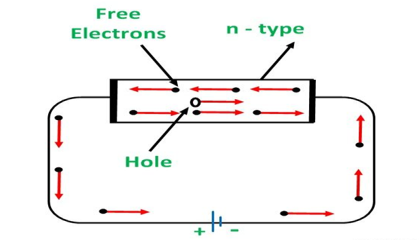
In the n-type semiconductor, a large number of free electrons are available in the conduction bands which are donated by the impurity atoms. The figure below shows the conduction process of an n-type semiconductor.
When a potential difference is applied across this type of semiconductor, the free electrons are directed towards the positive terminals. It carries an electric current. As the flow of current through the crystal is constituted by free electrons which are carriers of negative charge, therefore, this type of conductivity is known as negative or n-type conductivity.
11 Figure: |
The electron-hole pairs are formed at room temperature. These holes which are available in small quantity in valence band also consist of a small amount of current. For practical purposes, this current is neglected.
A P-N Junction Diode is formed by doping one side of a piece of silicon with a P-type dopant (Boron) and the other side with a N-type dopant (phosphorus). Ge can be used instead of Silicon. The P-N junction diode is a two-terminal device. This is the basic construction of the P-N junction diode. It is one of the simplest semiconductor devices as it allows current to flow in only one direction.
ZERO BIASED CONDITION
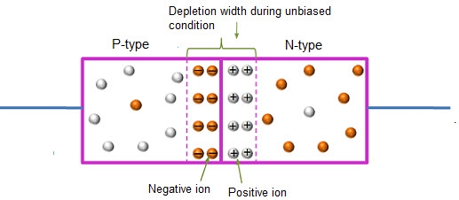
In this case, no external voltage is applied to the P-N junction diode; and therefore, the electrons diffuse to the P-side and simultaneously holes diffuse towards the N-side through the junction, and then combine with each other. Due to this an electric field is generated by these charge carriers. The electric field opposes further diffusion of charged carriers so that there is no movement in the middle region. This region is known as depletion width or space charge.
12 Figure: Unbiased or zero biased PN Junction Diode |
FORWARD BIAS
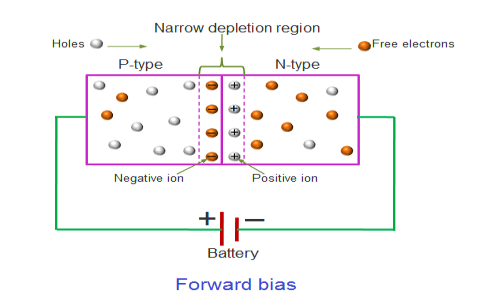
In the forward bias condition, the positive terminal of the battery is connected to the P-Type material and the negative terminal of the battery is connected to the N-type material. This connection is also called as giving positive voltage.
13 Figure: |
Electrons from the N-region cross the junction and enters the P-region. Due to the attractive force that is generated in the P-region the electrons are attracted and move towards the positive terminal. Simultaneously the holes are attracted to the negative terminal of the battery. By the movement of electrons and holes current flows. In this condition, the width of the depletion region decreases due to the reduction in the number of positive and negative ions.
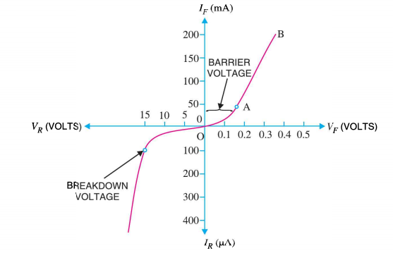
If this external voltage Vf becomes greater than the value of the potential barrier, approx. 0.7 volts for silicon and 0.3 volts for germanium, the potential barriers opposition will be overcome and current will start to flow.
This is because the negative voltage pushes or repels electrons towards the junction giving them the energy to cross over and combine with the holes being pushed in the opposite direction towards the junction by the positive voltage. This results in a characteristics curve of zero current flowing up to this voltage point, called the “knee” on the static curves and then a high current flow through the diode with little increase in the external voltage as shown in I-V characteristics.
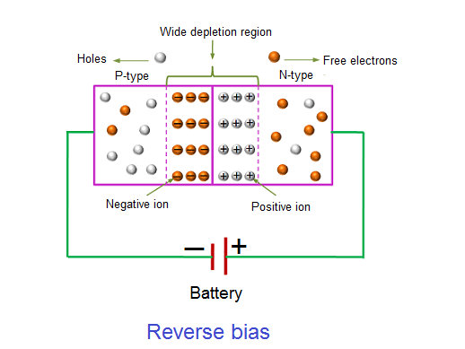
REVERSE BIAS
In the forward bias condition, the negative terminal of the battery is connected to the N-type material and the positive terminal of the battery is connected to the P-type material. This connection is also known as giving positive voltage. Hence, the electric field due to both the voltage and depletion layer is in the same direction. This makes the electric field stronger than before. Due to this strong electric field, electrons and holes want more energy to cross the junction so they cannot diffuse to the opposite region. Hence, there is no current flow due to the lack of movement of electrons and holes.
14 Figure: |
The positive voltage applied to the N-type material attracts electrons towards the positive electrode and away from the junction, while the holes in the P-type end are also attracted away from the junction towards the negative electrode.
The net result is that the depletion layer grows wider due to a lack of electrons and holes and presents a high impedance path, almost an insulator. The result is that a high potential barrier is created thus preventing current from flowing through the semiconductor material.
This condition represents a high resistance value to the PN junction and practically zero current flows through the junction diode with an increase in bias voltage. However, a very small leakage current does flow through the junction which can be measured in micro-amperes, ( μA ).
If the reverse bias voltage Vr applied to the diode is increased to a sufficiently high enough value, it will cause the diode’s PN junction to overheat and fail due to the avalanche effect around the junction. This may cause the diode to become shorted and will result in the flow of maximum circuit current, and this shown as a step downward slope in the reverse static characteristics curve in I-V characteristics.
I-V CHARACTERISTICS OF PN JUNCTION DIODE
The I-V Characteristic Curves, which is short for Current-Voltage Characteristic Curves or simply I-V curves of an electrical device
The application of a forward biasing voltage on the junction diode results in the depletion layer becoming very thin and narrow which represents a low impedance path through the junction thereby allowing high currents to flow. The point at which this sudden increase in current takes place is represented on the static I-V characteristics curve above as the “knee” point. The current starts increasing with increase in voltage. At knee voltage current shows a sharp increment in its magnitude. This behaviour us mentioned above. As large current flow in forward biasing so we measure this current in mA.
When a junction diode is Reverse Biased, the thickness of the depletion region increases and the diode acts like an open circuit blocking current flow. So only a very small leakage current will flow.
15 Figure: I-V chracteristics |
The photovoltaic effect is a process that generates voltage or electric current in a photovoltaic cell when it is exposed to sunlight. It is this effect that makes solar panels useful, as it is how the cells within the panel convert sunlight to electrical energy. The photovoltaic effect was first discovered in 1839 by Edmond Becquerel. When doing experiments involving wet cells, he noted that the voltage of the cell increased when its silver plates were exposed to the sunlight
The photovoltaic effect occurs in solar cells. These solar cells are composed of two different types of semiconductors - a p-type and an n-type - that are joined together to create a p-n junction. By joining these two types of semiconductors, an electric field is formed in the region of the junction as electrons move to the positive p-side and holes move to the negative n-side. This field causes negatively charged particles to move in one direction and positively charged particles in the other direction.
A solar cell or photo-voltaic cell is an electronic device that directly converts sun’s energy into electricity. When sunlight falls on a solar cell, it produces both a current and a voltage to produce electric power.
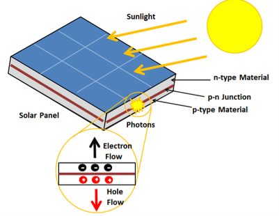
16 Figure: Solar Cell |
Light is composed of photons, which are simply small bundles of electromagnetic radiation or energy. These photons can be absorbed by a photovoltaic cell - the type of cell that composes solar panels. When light of a suitable wavelength is incident on these cells, energy from the photon is transferred to an atom of the semiconducting material in the p-n junction. Specifically, the energy is transferred to the electrons in the material. This causes the electrons to jump to a higher energy state known as the conduction band. This leaves behind a "hole" in the valence band that the electron jumped up from. This movement of the electron as a result of added energy creates two charge carriers, an electron-hole pair
When unexcited, electrons hold the semiconducting material together by forming bonds with surrounding atoms, and thus they cannot move. However in their excited state in the conduction band, these electrons are free to move through the material. Because of the electric field that exists as a result of the p-n junction, electrons and holes move in the opposite direction as expected. Instead of being attracted to the p-side, the freed electron tends to move to the n-side. This motion of the electron creates an electric current in the cell. Once the electron moves, there's a "hole" that is left. This hole can also move, but in the opposite direction to the p-side. It is this process which creates a current in the cell. A diagram of this process can be seen in Figure
It was first discovered by the Dutch physicist Heike Kamerlingh Onnes, who was the first to liquefy helium (which boils at 4.2 Kelvin at standard pressure).
In 1911 Kamerlingh Onnes and one of his assistants discovered the phenomenon of superconductivity while studying the resistance of metals at low temperatures. They studied mercury because very pure samples could easily be prepared by distillation. The historic measurement of superconductivity in mercury is shown in Figure.
17 Figure: |
The electrical resistance of mercury decreased steadily upon cooling, but dropped suddenly at 4.2 K, and became undetectably small.
Transition Temperature or Critical Temperature Tc
The temperature at which electrical resistivity of the material suddenly drops to zero and the material changes from normal conductor to a superconductor is called the transition temperature or critical temperature Tc.
Soon after this discovery, many other elemental metals were found to exhibit zero resistance when their temperatures were lowered below a certain characteristic temperature of the material, called the critical temperature, Tc.
Superconductivity
The ability of certain metals, their compounds and alloys to conduct electricity with zero resistance at very low temperature is called superconductivity. The materials which exhibit this property are called superconductors.
PROPERTIES
Following properties are shown by superconductors.
- It is a low temperature phenomenon.
- The electrical resistivity drops to zero.
- The conductivity becomes infinity.
- The transition temperature is different for different substances.
- Material having high normal resistivity exhibit superconductivity.
- Materials for which ρZ= 106 (where Z is a atomic number and ρ is resistivity) show superconductivity.
- Superconductivity is very sharp for chemically pure and structurally perfect specimen.
- Ferro magnetic and Anti ferromagnetic materials are not superconductors.
- Below the transition temperature the magnetic flux lines are rejected out of the superconductors.
- Generally Superconducting elements lie in the inner columns of the periodic table.
- Those metallic elements having their valence electrons lies between 2 to 8 exhibit superconductivity.
- Below the transition temperature the specific heat curve is discontinuous.
- There is a discontinuous change in specific heat.
- There are small changes in volume and thermal conductivity of the material.
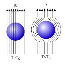
In 1933, Walter Meissner and Robert Ochsenfeld discovered a magnetic phenomenon that showed that superconductors are not just perfect conductors.
When a weak magnetic is applied to a superconducting specimen at a temperature below transition temperature Tc the magnetic flux lines are expelled. This phenomenon is called Meissner effect.
18 Figure: |
Under normal state the magnetic induction inside the specimen is
B = μ0(H+I)
Where H is the external applied magnetic field and I is the magnetization produced inside the specimen.
When the specimen is in superconducting state B=0 (Meissner effect)
B = μ0(H+I)
0 = μ0(H+I)
H= -I
χ = H/I =-1
Thus the material is act as a perfectly diamagnetic because for diamagnetic material susceptibility χ = -1 .
Let us consider a superconducting material is in normal state. From ohms law, the electric field E=Jρ
On cooling the material to its transition temperature ρ tends to zero. If J is held finite E must be zero. From Maxwell’s equations
∇ × E = - dB / dt
Under superconducting condition
Since E is zero
dB/dt =0
or B=constant.
This means that the magnetic flux passing through the specimen should not change on cooling to the transition temperature. The Meissner effect contradicts the result.
Application of Meissner Effect
This effect of superconductivity is used in magnetic levitation which is the base of modern high-speed bullet trains. In superconducting state (phase), due to expulsion of external magnetic field, the sample of superconducting material levitates above magnet or vice-versa. Modern high-speed bullet trains use the phenomenon of magnetic levitation.
Based on the diamagnetic response superconductors can be classified into two types, they are
1. Type I superconductors
2. Type II superconductors.
- TYPE I SUPERCONDUCTORS
Superconductors which one follows a complete Meissner effect is called type I superconductors. It is also known as soft superconductors.
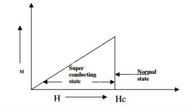
When the magnetic field strength is gradually increased from its initial value H < HC at HC the diamagnetism is abruptly disappear and the transition from superconducting state to normal state is sharp as shown in figure. These superconductors are known as soft superconductors.
Examples: - Al, Zn, Hg and Sn
19 Figure: Type I superconductors |
2. TYPE II SUPERCONDUCTORS
Superconductors which does not follow the complete Meissner effect is called type I superconductors. It is also known as hard superconductors.
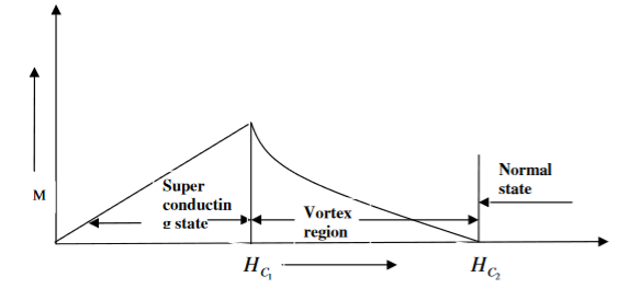
In type II superconductors, the specimen is in pure superconducting state up to the field HC1 (lower critical field) when the field is increased beyond HC2 (upper critical state) the magnetic flux lines start penetrating.
The specimen is in mixed state between HC1 and HC2. Above HC2, the specimen is in normal state. This means that the Meissner effect is incomplete in the region between HC1 and HC2. This region is known as vertex region. These superconductors are known as hard superconductors.
Examples: - Zr, Nb
20 Figure: Type II superconductors |
DIFFERENCES BETWEEN TYPE I AND TYPE II SUPERCONDUCTOR
Type I superconductor | Type II superconductor |
1. It follows complete Meissner effect. | 1. It does not follow the complete Meissner effect |
2. It has single critical field valueHC | 2. It has two critical field values HC1 and HC2. |
3. There no mixed state. | 3. There is a mixed state |
4. They are soft superconductors | 4. They are hard superconductors |
5. Materials with pure form are type I superconductors | 5. Materials with impurities or alloys are type II superconductors |
BCS theory of superconductor was put forward by Bardeen, Cooper and Schrieffer in 1957 and hence named as BCS theory. This theory could explain the effects such as zero resistivity, Meissner effect, isotopic effect etc. Electron lattice interaction via lattice deformation.
ELECTRON –PHONON INTERACTION
BCS theory showed that the basic interaction responsible for superconductivity appears to be that of a pair of electrons by means of an interchange of virtual phonons. This is explained as follows:-
Suppose an electron approaches a positive ion core. It suffers attractive coulomb interaction. Due to this attraction ion core is set in motion and thus distorts that lattice. Let a second electron come in the way of distorted lattice and interaction between the two occurs which lowers the energy of the second electron. The two electrons therefore interact indirectly, via lattice distortion or the phonon field, thus lowering the energy of electrons. This type of interaction is called electron-lattice is quantized in terms of phonons the above interaction can also be interpreted as electron –electron interaction through phonons.
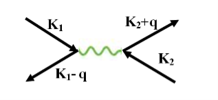
Let an electron of wave vector K emits phonon q, which is absorbed by an electron of wave number K. K is thus scattered as K-q and the process being a virtual one. The nature of the resulting electron-electron interactions depends on the relative magnitudes of the electronic energy change and the phonon energy. If this phonon energy exceeds electronic energy, the interaction is attractive.
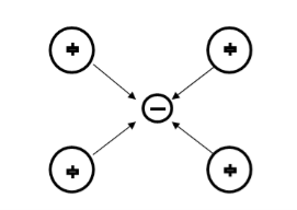
Let us consider an electron is passing through the lattice positive ions. The electron is attracted by the neighbouring lattice positive ions as shown in figure 1. Due to the attraction of electron and ion core, the lattice gets deformed on scale. So electron get partially positive charge. Now if another electron passes by the side of assembly of said electron and ion core, it gets attracted towards the assembly.
21 Figure |
The second electron interacts with the first electron due to the exchange of virtual photon q, between two electrons. The interaction process can be written in terms the wave vector k as
22 Figure |
k1’ =k1–q k2’ = k2+q
These two electrons together form a cooper pair and is known as cooper electron.
COOPER PAIRS
To understand the mechanism of cooper pair formation, let us consider the distribution of electrons in metals as given by the Fermi-Dirac distribution function.
F(E) = 1/ 1+ e E-EF/kT
At T= 0K, all the Fermi energy states below the Fermi level are completely filled and all the states above are completely empty. Let us see what happens when two electrons are added to a metal at absolute zero. Since all the quantum states E<EF, are filled, they are forced to occupy states having E>EF.
Cooper showed that if there an attraction between the two electrons, they are able to form a bound state so that their total energy is less than 2EF. These two electrons are paired to form a single system. These two electrons form a cooper pair and is known as cooper electron.
COHERENCE LENGTH
The paired electrons are not scattered and can maintain their coupled motion up to certain distance called the coherence length. It is a measure of the distance within which the gap parameter does not change very much in varying magnetic field.
The high-Tc superconductors are the class of materials with the highest recorded transition temperatures, on the order of 100 K and above. Discovered over 20 years ago, there remain a number of unanswered questions about these compounds.
The first high temperature superconductor was discovered in 1986, by IBM researchers Bednorz and Müller,who were awarded the Nobel Prize in Physics in 1987 "for their important break-through in the discovery of superconductivity in ceramic materials".
High-temperature superconductors (abbreviated high-Tc or HTS) are operatively defined as materials that behave as superconductors at temperatures above 77 K (−196.2 °C; −321.1 °F), the boiling point of liquid nitrogen, one of the simplest coolants in cryogenics. All superconducting materials known at ordinary pressures currently work far below ambient temperatures and therefore require cooling. The majority of high-temperature superconductors are ceramic materials. On the other hand, Metallic superconductors usually work below -200 °C: they are then called low-temperature superconductors. Metallic superconductors are also ordinary superconductors, since they were discovered and used before the high-temperature ones.
Ceramic superconductors are now becoming suitable for some practical use, but they still have many manufacturing issues and there are very few successful practical examples of employment. Most ceramics are brittle which makes the fabrication of wires from them very problematic.
The major advantage of high-temperature ceramic superconductors is that they can be cooled by using liquid nitrogen. On the other hand, metallic superconductors usually require more difficult coolants - mostly liquid helium. Unfortunately, none of high-temperature superconductors are cool able using only dry ice, and none of them works at room temperature and pressure (they work well below the lowest temperature recorded on Earth). All high-temperature superconductors require some kind of cooling systems.
The main class of high-temperature superconductors are in the class of copper oxides (only some particular copper oxides). The second class of high-temperature superconductors in the practical classification is the class of iron-based compounds. Magnesium diboride is sometimes included in high-temperature superconductors: it is relatively simple to manufacture, but it super conducts only below −230 °C, which makes it unsuitable for liquid nitrogen cooling (approximately 30 °C below nitrogen triple point temperature). For example, it can be cooled with liquid helium, which works at much lower temperatures.
Many ceramic superconductors physically behave as superconductors of the second type.
Some extremely-high pressure superhydride compounds are usually categorized as high-temperature superconductors. In fact, many articles on high-temperature superconductors can be found on this research on high pressure gases, which is not suitable for practical applications. The current TC record holder is lanthanum decahydride.
One of the key mysteries surrounds the identity of the so-called 'pseudo gap' region of the phase diagram. In this regime there exists a gap like feature observed in many physical quantities, yet there is no obvious signs of an ordered phase. Some of the research in the group has been directed at studying the specific heat of the high-Tc's in the pseudogap region of the phase diagram.
A second intriguing question surrounds how the high-Tc's evolve with charge carrier concentration (doping), moving from an antiferromagnetically ordered insulator at low doping, to an unconventional superconductor and eventually a Fermi liquid metal at higher doping. At low dopings, there is evidence for a 'glassy' behaviour of electronic spins, and part of the research effort is directed towards exploring this region of the phase diagram through muon-spin relaxation, transport and dielectric measurements.
HALL EFFECT
When magnetic field is applied perpendicular to a current-carrying conductor, then a voltage is developed in the material perpendicular to both magnetic field and current in the conductor. This effect is known as Hall Effect and the voltage developed is known as Hall voltage (VH).
Hall Effect is useful to identify the nature of charge carriers in a material and hence to decide whether the material is n-type semiconductor or p-type semiconductor, also to calculate carrier concentration and mobility of carriers.
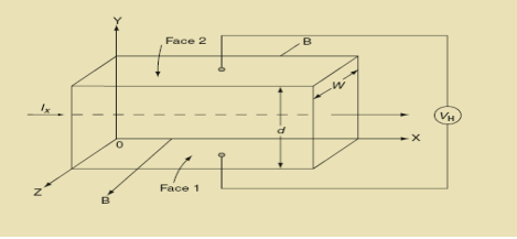
Hall Effect can be explained by considering a rectangular block of an extrinsic semiconductor in which current is flowing along the positive X-direction and magnetic field B is applied along Z-direction as shown in Figure.
22 Figure: Hall Effect |
Suppose if the semiconductor is n-type, then mostly the carriers are electrons and the electric current is due to the drifting of electrons along negative X-direction or if the semiconductor is p-type, then mostly the carriers are holes and the electric current is due to drifting of the holes along positive X-direction.
As these carriers are moving in magnetic field in the semiconductor that mean they experience Lorentz force represented by FL
FL = Bevd
Where vd is the drift velocity of the carriers. (already explained in previous section).
We can obtain the direction of this force by applying Fleming’s left-hand rule in electromagnetism.
Fleming’s left-hand rule can be explained as If we stretch the thumb, fore finger and middle finger in three perpendicular directions so that the fore finger is parallel to the magnetic field and the middle finger is parallel to the current direction, then thumb represents the direction of force on the current-carrying carriers.
So the Lorentz force is exerted on the carriers in the negative Y-direction. Due to Lorentz force, more and more carriers will be deposited at the bottom face (represented by face 1in figure) of the conductor.
The deposition of carriers at the bottom face is continued till the repulsive force due to accumulated charge balances the Lorentz force.
After some time of the applied voltage, both the forces become equal in magnitude and act in opposite direction, then the potential difference between the top and bottom faces is equal to Hall voltage and that can be measured.
At equilibrium, the Lorentz force on a carrier FL = Bevd ……………..(1) and the Hall force FH = eEH ……………..(2) Where EH is the Hall electric field due to accumulated charge. At equilibrium, FH = FL eEH = Bevd ∴ EH = Bvd ……………..(3) If ‘d’ is the distance between the upper and lower surfaces of the slab, then the Hall field EH = In n-type material, Jx = –nevd vd = - Where n is free electron concentration, substituting (5) in (3), we have ∴ EH = -B For a given semiconductor, the Hall field EH is proportional to the current density Jx and the intensity of magnetic field ‘B’ in the material. i.e. EH ∝ JxB (or) EH = RHJxB ……………..(7) Where RH = Hall coefficient Equations (6) and (7) are same so, we have RHJxB =-B RH = - Where ρ is charge density Similarly for p-type material RH = Using Equations (8) and (9), carrier concentration can be determined. |
Thus, the Hall coefficient is negative for n-type material. In n-type material, as more negative charge is deposited at the bottom surface, so the top face acquires positive polarity and the Hall field is along negative Y-direction. The polarity at the top and bottom faces can be measured by applying probes.
Similarly, in case of p-type material, more positive charge is deposited at the bottom surface. So, the top face acquires negative polarity and the Hall field is along positive Y-direction. Thus, the sign of Hall coefficient decides the nature of (n-type or p-type) material.
The Hall coefficient can be determined experimentally in the following way: Multiplying Equation (7) with ‘d’, we have EHd = VH = RHJxBd ……………..(10) From (Figure 11) we know the current density Jx Jx = Where W is width of the box. Then, Equation (10) becomes VH = RH RH = Substituting the measured values of VH, Ix, B and W in Equation(11), RH is obtained. The polarity of VH will be opposite for n- and p-type semiconductors. The mobility of charge carriers can be found by using the Hall effect, for example, the conductivity of electrons is n = neμn Or we can rewrite it as μn = by using equation (11) μn = n |
HALL EFFECT APPLICATIONS
• Using magnetic flux leakage – In order to properly inspect items such as pipes or tubes, Hall Effect probes work with something called magnetic flux leakage. This is a way of testing such items, and being able to spot potential corrosion, erosion, or pitting. This is specifically used in steel items, and can give important information about lifespan or safety.
• Sensors to detect rotation speed – A Hall Effect probe can be used to in bicycle wheels, speedometers in the automotive world, electronic types of ignition systems, and gear teeth.
• Used to detected movement – You will often find a Hall Effect probe used in such items as Go-Kart controls, smart phones, paintball guns, or airsoft guns, as well as some GPS systems.
• Ferrite Toroid Hall Effect current transducers – This is mainly used in electronic compasses, making use of the magnetic field to show direction.
• Split-ring clamp-on sensors – These types of Hall Effect probes are used to test equipment without having to take the whole circuit board apart, e.g. complex items.
• Analog multiplication – Anything which needs a power measurement, e.g. sensing, and also used in small computers.
• General power measurement – Basically any device which needs to be tested for its power input can be done by a Hall Effect probe.
• Position and motion sensors – This is mainly used in a DC motor, often the brushless type.
• The automotive world – Hall Effect probes are used widely in the automotive world, especially in fuel injection and ignition. Wheel rotation sensors also use Hall Effect probes, e.g. for anti-lock braking.
- For determination of type of given semiconductor.
- For N-type, Hall coefficient RH= negative
- For P-type, Hall coefficient RH= Positive
- To determine carrier concentration n and p; that is n=p=1/e𝑅𝐻
- Determination of mobility of charge carriers μn =
 =n RH. Where 𝜎= electrical conductivity
 - To determine the sign of charge carriers whether the conductivity is due to electrons or holes.
Main Advantages of Using Hall Sensors
Why is a Hall Effect probe advantageous in all of these instances? Because the probes are not affected by outside influences, e.g. water or dirt. They can also easily sense the measure the output they need when they are placed in the right position. On top of this, Hall Effect probes are safer, because the voltage never actually makes it directly to the sensor/probe. This makes this type of measurement overall so much safer than other methods.
As you can see, understanding how something is put in practice in the real world really helps you to understand it in real terms. The Hall Effect is certainly very common place these days, in much more methods and applications than we realize. While certainly very useful in the automation world, even basic items such as a compass make large use of this scientific approach.
SOLID-STATE LASERS (RUBY LASER)
RUBY LASER
Ruby laser is a three level solid state laser and was constructed by Maiman in 1960. Ruby laser is one of the few solid-state lasers that produce visible light. It emits deep red light of wavelength 694.3 nm.
CONSTRUCTION
A ruby laser consists of three important elements: laser medium, the pump source and the optical resonator.
Laser Medium
Ruby (Al2O3+Cr2O3) is a crystal of Aluminium oxide, in which 0.05% of Al+3 ions are replaced by the Cr+3 ions. The colour of the rod is pink. The active medium or laser medium in the ruby rod is Cr+3 ions. In ruby laser 4cm length and 5mm diameter rod is generally used. The ruby has good thermal properties.
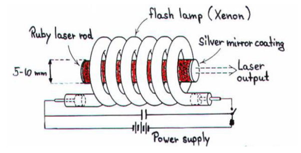
23 Figure |
The pump source
The ruby rod is surrounded by xenon flash tube, which provides the pumping light to excite the chromium ions in to upper energy levels. The ruby rod was surrounded by a helical xenon flash lamp.
We know that population inversion is required to achieve laser emission. Population inversion is the process of achieving the greater population of higher energy state than the lower energy state. In order to achieve population inversion, we need to supply energy to the laser medium i.e. to ruby crystal.
Xenon flash tube emits thousands joules of energy in few milliseconds, but only a part of that energy is utilized by the chromium ions while the rest energy heats up the apparatus. A cooling arrangement is provided to keep the experimental set up at normal temperatures.
Optical resonator
Both the ends of the rods are highly polished and made strictly parallel. The ends are silvered in such a way, one becomes partially reflected the laser beam was emitted through that end and the other end fully reflected to reflect all the rays of light striking it.
WORKING OF RUBY LASER:
Consider a ruby laser medium consisting of three energy levels E1, E2, E3 with N number of electrons.
We assume that the energy levels will be E1 < E2 < E3. The energy level E1 is known as ground state or lower energy state, the energy level E2 is known as metastable state, and the energy level E3 is known as pump state.
Let us assume that initially most of the electrons are in the lower energy state (E1) and only a tiny number of electrons are in the excited states (E2 and E3).
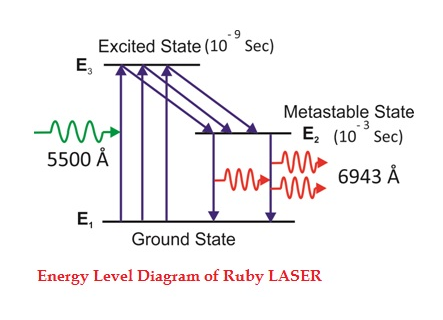
The energy level diagram of chromium ions is shown in figure. The chromium ions get excitation into higher energy levels by absorbing of 5500Å of wavelength radiation. The excited chromium ions stay in the level E3 for short interval of time (10-8 to 10-9 Sec). After their life time most of the chromium ions are de-excited from E3 to E1 and a few chromium ions are de-excited from E3 to E2.
24 Figure |
The transition between E3 and E2 is non-radioactive transition i.e. the chromium ions gives their energy to the lattice in the form of heat. In the Meta stable state the life time of chromium ions is 10-3 sec. The life time of chromium ions in the Meta stable state is 105 times greater than the life time of chromium ions in higher state.
Due to the continuous working of flash lamp, the chromium ions are excited to higher state E3 and returned to E2 level. After few milliseconds the level E2 is more populated than the level E1 and hence the desired population inversion is achieved. The state of population inversion is not a stable one. The process of spontaneous transition is very high. When the excited chromium ion passes spontaneously from E3 to E2it emits one photon of wave length 6943 Å. The photon reflects back and forth by the silver ends and until it stimulates an excited chromium ion in E2 state and it to emit fresh photon in phase with the earlier photon. The process is repeated again and again until the laser beam intensity is reached to a sufficient value. When the photon beam becomes sufficient intense, it emerges through the partially silvered end of the rod. The wave length 6943 Å is in the red region of the visible spectrum.
DRAW BACKS OF RUBY LASER
- The laser requires high pumping power
- The efficiency of ruby laser is very small
- It is a pulse laser
APPLICATION OF RUBY LASER
- Ruby lasers are in optical photography
- Ruby lasers can be used for measurement of plasma properties such as electron density and temperature.
- Ruby lasers are used to remove the melanin of the skin.
- Ruby laser can be used for recording of holograms.
ND: YAG SOLID LASER
Neodymium-doped Yttrium Aluminum Garnet (Nd: YAG) laser is a solid state laser in which Nd: YAG is used as a laser medium.
These lasers have many different applications in the medical and scientific field for processes such as Lasik surgery and laser spectroscopy.
Nd: YAG laser is a four-level laser system, which means that the four energy levels are involved in laser action. These lasers operate in both pulsed and continuous mode.
Nd: YAG laser generates laser light commonly in the near-infrared region of the spectrum at 1064 nanometers (nm). It also emits laser light at several different wavelengths including 1440 nm, 1320 nm, 1120 nm, and 940 nm.
ND: YAG LASER CONSTRUCTION
Nd:YAG laser consists of three important elements: an energy source, active medium, and optical resonator.
Energy source
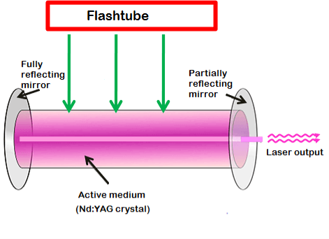
The energy source or pump source supplies energy to the active medium to achieve population inversion. In Nd: YAG laser, light energy sources such as flashtube or laser diodes are used as energy source to supply energy to the active medium.
In the past, flashtubes are mostly used as pump source because of its low cost. However, nowadays, laser diodes are preferred over flashtubes because of its high efficiency and low cost.
25 Figure |
Active medium
The active medium or laser medium of the Nd:YAG laser is made up of a synthetic crystalline material (Yttrium Aluminum Garnet (YAG)) doped with a chemical element (neodymium (Nd)). The lower energy state electrons of the neodymium ions are excited to the higher energy state to provide lasing action in the active medium.
Optical resonator
The Nd:YAG crystal is placed between two mirrors. These two mirrors are optically coated or silvered.
Each mirror is silvered or coated differently. One mirror is fully silvered whereas, another mirror is partially silvered. The mirror, which is fully silvered, will completely reflect the light and is known as fully reflecting mirror.
On the other hand, the mirror which is partially silvered will reflect most part of the light but allows a small portion of light through it to produce the laser beam. This mirror is known as a partially reflecting mirror.
WORKING OF ND: YAG LASER
Nd: YAG laser is a four-level laser system, which means that the four energy levels are involved in laser action. The light energy sources such as flashtubes or laser diodes are used to supply energy to the active medium.
In Nd:YAG laser, the lower energy state electrons in the neodymium ions are excited to the higher energy state to achieve population inversion.
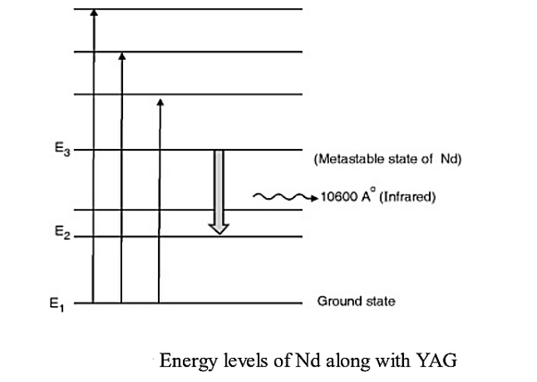
Consider a Nd:YAG crystal active medium consisting of four energy levels E1, E2, E3, and E4 with N number of electrons. The number of electrons in the energy states E1, E2, E3, and E4 will be N1, N2, N3, and N4.
Let us assume that the energy levels will be E1 < E2 <E3 <E4. The energy level E1 is known as ground state, E2 is the next higher energy state or excited state, E3 is the metastable state or excited state and E4 is the pump state or excited state. Let us assume that initially, the population will be N1 > N2 > N3 > N4.
E1 is ground state and E3 offers metastable state. Pumping takes place with light of wavelength 5000 A° to 8000 A° which excites Nd+3 ions to higher states. The metastable state E3 rapidly gets populated due to downward transitions from higher energy levels as none of them is metastable. Population inversion takes place between E3 and E2. A continuous laser of 10600 A° in infrared region is given out due to stimulate emission taking place between E3 and E2.
26 Figure |
ADVANTAGES OF ND:YAG LASER
- Low power consumption
- Nd:YAG laser offers high gain.
- Nd:YAG laser has good thermal properties.
- Nd:YAG laser has good mechanical properties.
- The efficiency of Nd:YAG laser is very high as compared to the ruby laser.
APPLICATIONS OF ND:YAG LASER
Military
Nd:YAG lasers are used in laser designators and laser rangefinders. A laser designator is a laser light source, which is used to target objects for attacking. A laser rangefinder is a rangefinder, which uses a laser light to determine the distance to an object.
Medicine
Nd: YAG lasers are used to correct posterior capsular opacification (a condition that may occur after a cataract surgery).
Nd:YAG lasers are used to remove skin cancers.
Manufacturing
Nd:YAG lasers are used for etching or marking a variety of plastics and metals.
Nd:YAG lasers are used for cutting and welding steel.
