Unit 4
Field Effect Transistor
FET is an acronym used for “field effect transistor”. It is a three terminal unipolar device in which conduction is manipulated with the help of applied electric field.
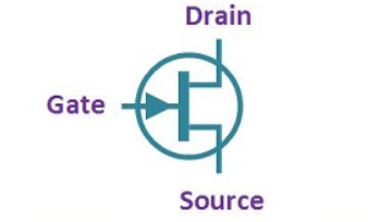
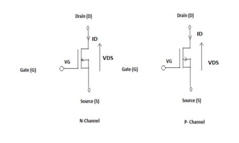
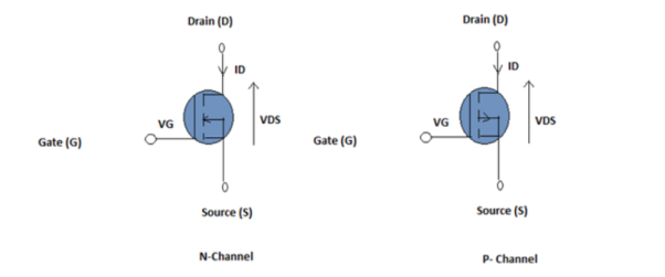
Thus, it is also referred as a voltage controlled device in which only majority charge carriers are involved in the conduction mechanism. It comprises of three terminals, i.e. source, gate, and drain. The circuit symbol described in the below diagram clearly illustrates the three terminals of field effect transistor.
|
Construction
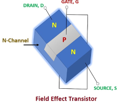
The semiconductor is the basis of all FETs. Depending on the channel we are using, i.e. N-channel or P-channel, the semiconductor specimen will be used. If we are designing N-channel JFETs, then the channel will be of an N-type semiconductor. And in the middle of the opposite phases of the specimen will be diffused with the P-type semiconductor.
|
The P-type semiconductor bar will act as a gate terminal. The opposite ends of the P-type semiconductor will be connected together to form a common gate terminal. Thus, there will be two P-N junctions on either side of the gate, and that will be termed as source and drain terminal.
Components of FETs
- Channel: This is the area in which majority charge carriers flow. When the majority charge carriers are entered in FET, then with the help of this channel only they flow from source to drain.
- Source: Source is the terminal through which the majority charge carriers are introduced in the FET.
- Drain: Drain is the collecting terminal in which the majority charge carriers enter and thus contribute in the conduction procedure.
- Gate: Gate terminal is formed by diffusion of a type of semiconductor with another type of semiconductor. It basically creates high impurity region which controls the flow of carrier from source to drain.
Working:
|
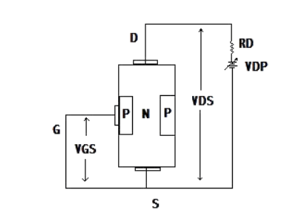
Gate are always reverse biased hence the gate current IG is practically zero. The source terminals is always connected to the end of the drain supply which provides necessary carrier ,in N-channel JFET source terminal is connected to the neagative end of the drain voltage source. The electrons flow from source to drain through the channel from D to S is started.
The current ID increases as Vdsincreases from zero on ward. This relationship between VDS and ID continuous till VDS reaches certain value called Pinch off
When VDS is equal to zero and VGS is decreased from zero the gate reverse bias increases , as the negative Vgs increases a stage reaches where two dip lections touch other in this condition the channel is said to be cut-off.
At a fixed drain voltage, the drain current (ID) of a JFET depends on the gate to source voltage (VGS). If the gate to source voltage decreases from zero in n channel JFET, the drain current also gets decreased accordingly. The relation between gate to source voltage and drain current is given below. ID = IDSS [ 1 – VGS/ VGS(off)] 2 After a certain gate to source voltage (VGS), the drain current ID becomes zero. This voltage is known as Cut Off Gate Voltage (VGS(off)). When the gate terminal is grounded (VGS = 0) and positive drain to source voltage (VDS) is being increased slowly in case of n channel JFET, the drain current gets increased linearly. But after pinch-off voltage (Vp), the drain current would not be increased further and gets a constant value. This is the maximum drain current that can flow through the channel when the gate terminal is in ground potential. This current is fixed for a JFET and this is called shorted gated drain current and generally denoted by IDSS.
Transconductance is the ratio of change in drain current (δID) to change in the gate to source voltage (δVGS) at a constant drain to source voltage (VDS = Constant). gm = ∂ ID/ ∂ VGS at constant VDS ID = IDSS [ 1 – VGS/ VGS(off)] 2 Dynamic Output Resistance This is the ratio of change of drain to source voltage (δVDS) to the change of drain current (δID) at a constant gate to source voltage (VGS = Constant). The ratio is
rd = ∂ VDS / ∂ ID at constant VGS
denoted as rd.
The amplification factor is defined as the ratio of change of drain voltage (δVDS) to change of gate voltage (δVGS) at a constant drain current (ID = Constant). μ=∂ VDS / ∂ VGS at constant ID
μ=∂ VDS / ∂ VGS = μ=∂ VDS / ∂ ID x ∂ ID / ∂ VGS
μ = rd x gm
JFET as a switch
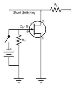
FET can be used as a switch by operating it in two regions, they are cutoff and saturation region. When the VGS is zero the FET operates in saturation region and maximum current flows through it. Hence it is like a fully switched ON condition. Similarly, when the VGS applied is more negative than the pinch off voltage, FET operates in cutoff region and doesn’t allow any current flow through the device. Hence FET is in fully OFF condition.
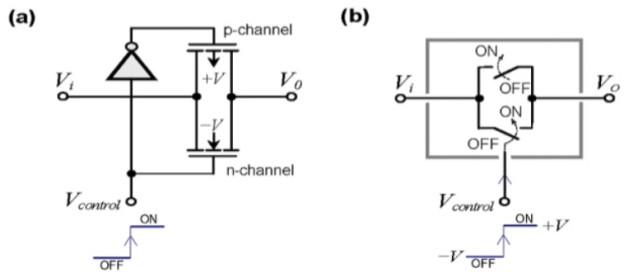
FET Used as a Shunt Switch
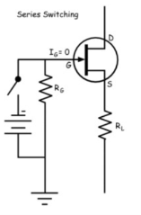
FET Used as a Series Switch
In this circuit FET acts as a series switch. It acts as a closed switch if the control voltage is zero and open switch if control voltage is negative. When the FET is ON, the input signal will appear at the output and when it is OFF the output is zero.
|
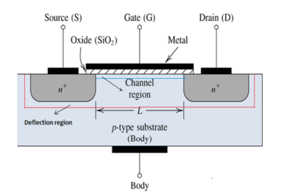
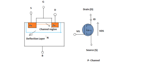
The MOSFET works by varying the width of a channel along which charge carriers flow (electrons or holes). The charge carriers enter the channel at source and exit via the drain. The width of the channel is controlled by the voltage on an electrode is called gate which is located between source and drain. It is insulated from the channel near an extremely thin layer of metal oxide. The MOS capacity present in the device is primary. The MOSFET can function in two ways
Depletion Mode:
When there is no voltage on the gate, the channel displays maximum conductance. As the voltage on the gate is either positive or negative, the channel conductivity decreases. Enhancement Mode When there is no voltage on the gate the device does not conduct. More is the voltage on the gate, the better the device can conduct.
Enhancement mode Working:
MOSFET construction P-channel MOSFET
Enhanced mode
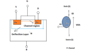
Depletion mode P-channel MOSFET
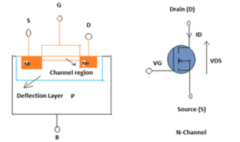
N- Channel MOSFET:
Enhancement mode
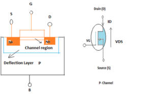
Depletion mode N channel MOSFET |
Sr No | Parameter Characteristics |
BJT |
JFET |
MOSFET |
1 | Current/voltage controlled device | Current controlled | Voltage controlled | Voltage controlled |
2 | Size | Small | Very small | Very small |
3 | Controlling terminal |
Base |
Gate |
Gate |
4 | Thermal runaway | Can take place | Does not take place | Does not take place |
5 | Transfer characteristics |
Linear |
Non linear |
Non linear |
6 | Input resistance | Low or High |
High |
Very High |
7 | Noise produced | High | Low | Very low |
PMOS Logic
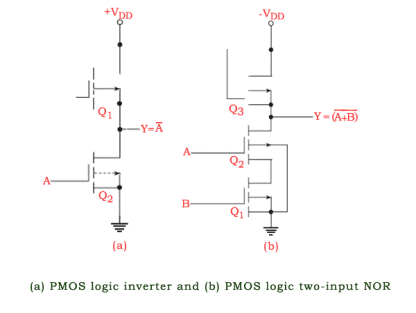
The PMOS logic family uses P-channel MOSFETS. Figure (a) shows an inverter circuit using PMOS logic .MOSFET Q1 acts as an active load for the MOSFET switch Q2. For the circuit shown,GND and −VDD respectively represent a logic ‘1’ and a logic ‘0’ for a positive logic system. When the input is grounded (i.e. logic ‘1’), Q2 remains in cut-off and −VDD appears at the output through the conducting Q1. When the input is at −VDD or near −VDD, Q2 conducts and the output goes to near-zero potential (i.e. logic ‘1’). Figure (b) shows a PMOS logic based two-input NOR gate. In the logic arrangement of Fig.(b), the output goes to logic ‘1’ state (i.e. ground potential) only when both Q1 and Q2 are conducting. This is possible only when both the inputs are in logic ‘0’ state. For all other possible input combinations, the output is in logic ‘0’ state, because, with either Q1 or Q2 nonconducting, the output is nearly −VDD through the conducting Q3. The circuit of Fig.(b) thus behaves like a two-input NOR gate in positive logic.
NMOS Logic
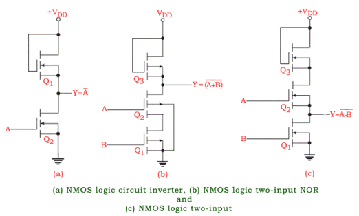
It is for this reason that most of the MOS memory devices and microprocessors employ NMOS logic or some variation of it such as VMOS, DMOS and HMOS. VMOS, DMOS and HMOS are only structural variations of NMOS, aimed at further reducing the propagation delay. Figures (a), (b) and (c) respectively show an inverter, a two-input NOR and a two-input NAND using NMOS logic.
CMOS:
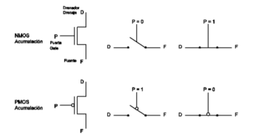
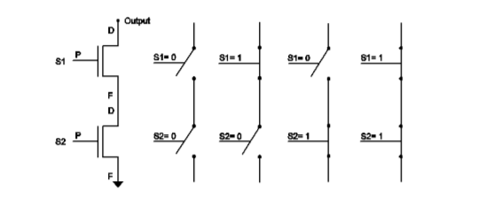
For NMOS transistors, if the input is a 1 the switch is on, otherwise it is off. On the other hand, for the PMOS, if the input is 0 the transistor is on, otherwise the transistor is off.
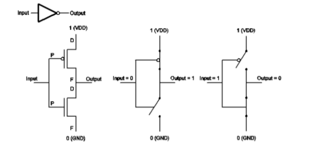
Here is a graphical representation of these facts: When a circuit contains both NMOS and PMOS transistors we say it is implemented in CMOS (Complementary MOS) . Understanding the basics of transistors, we can now design a simple NOR gate.
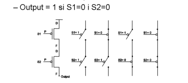
Next figure shows the implementation in transistors of the NOR gate and how it works for different inputs (1 and 0). On the left there is the implementation, on the right the behavior. The symbol VDD is the source voltage (or the logic 1), GND is the ground (or the logical 0). To implement the rest of logical gates we analyze first the behavior of the transistors when connected in a “series” fashion or in a “parallel” way. If we connect two NMOS transistors in series, we get the behaviour shown in next figure (the triangle in the bottom is a graphical representation of GND)
Next figure shows the behavior of the PMOSes when connected in series. (The horizontal line on top of the first transistor is a graphical representation of VDD).
|
|
CMOS circuits are constructed in such a way that all PMOS transistors must have either an input from the voltage source or from another PMOS transistor.
All NMOS transistors must have either an input from ground or from another NMOS transistor.
Reference Books:
1. V. N. Mittal, Arvind Mittal, ‘Basic Electrical Engineering’, Tata McGraw Hill publishing co. ltd, New Delhi.
2. D. P. Kothari, I.J Nagrath, ‘Basic Electrical Engineering’, Tata McGraw Hill
3. M. S. Naidu, S. Kamakshaiah, ‘Introduction to Electrical Engineering’, Tata McGraw Hill.
4. P. Tiwari, ‘Basic Electrical Engineering’, New Age Publication.
5. Vincent Del Toro, ‘Electrical Engineering Fundamentals’, Pearson
6. R. P. Jain, ‘Modern Digital Electronics’ McGraw Hill Education (India) Private Limited, Fourth Edition, 2017.
7. B. L. Theraja, ‘Applied Electronics’ S. Chand Publication
8. A.P. Malvino, ‘Electronics Principles’ TMH Publications.
