Unit 5
Silicon Controlled Rectifier
SCR (Silicon Controlled Rectifier)
- The silicon controlled rectifier ( SCR ) is a three terminal semiconductor switching device which can be used as a controlled switch to perform various functions such as rectification, inversion and regulation of power flow.
- An SCR can handle currents up to several thousand amperes and voltages up to more than 1kV.
- Similar to the diode, SCR is a unidirectional device that conducts current in one direction only, but unlike a diode, the SCR operates as either an open-circuit switch or as a rectifying diode depending upon how its gate is triggered.
- SCR can operate only in the switching mode and cannot be used for amplification.
- Hence, used extensively in switching d.c. and a.c., rectifying a.c
to give controlled output, converting d.c. into a.c. etc.
Construction
When a p-n junction is added to a junction transistor, the resulting three p-n junctions device is called a silicon controlled rectifier.
The construction of an SCR. is as shown in the figure.
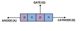
Three terminals are :
- The outer p-type material called anode A
- The outer layer of n-type material called cathode K
- The third from the base of transistor section called gate G.
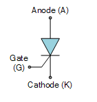
The symbol of SCR is as shown in figure:
Working :
In SCR the load is connected in series with anode. The anode is always kept at positive potential with respect to cathode.
When gate is open:
|
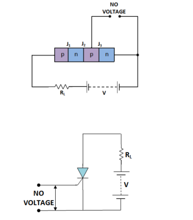
SCR circuit with gate open that is no voltage applied to the gate.
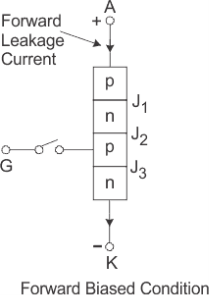
- Under this condition, junction J2 is reverse biased while junction J1 and J3 are forward biased.
- Hence, the situation in the junctions J1 and J3 is just as in a npn transistor with base open.
- Therefore no current flows through the load RL and SCR is cut-off.
- If the applied voltage is gradually increased, a stage will be reached when the reverse biased junction breaks down and SCR conducts heavily and is said to be ON state.
- The applied voltage at which SCR conducts heavily without the gate voltage is called Break-over voltage.
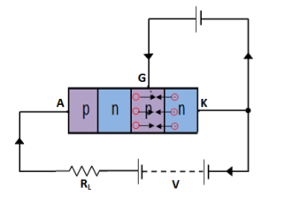
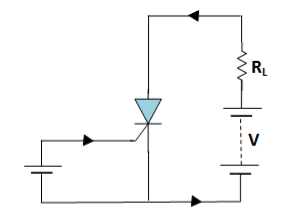
- When the gate voltage is positive with respect to cathode
When a small positive voltage is applied to gate the SCR is made to conduct heavily with respect to the small applied voltage.
|
- The electrons from n-type material start to move across junction J3 towards left whereas holes from p-type towards the right.
- Consequently, the electrons from junction J3 are attracted across the junction J2 and gate current starts flowing.
- As soon as the gate current flows, anode current increases.
- The increased current in turn makes more electrons available at junction J2.
- This process continues and in an extremely small time, junction J2 breaks down and the SCR starts conducting heavily.
- Once SCR starts conducting, the gate loses all control. Even if gate voltage is removed, the anode current does not decrease at all.
- The only way to stop conduction to bring the SCR to off condition is to reduce the applied voltage to zero.
- Characteristics:
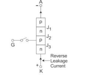
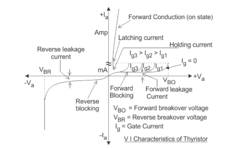
Initially for the reverse blocking mode of the thyristor, the cathode is made positive with respect to anode by supplying voltage E and the gate to cathode supply voltage Es is detached initially by keeping switch S open.
|
J1 and J3arenow forward biased but junction J2 goes into reverse biased condition. In this particular mode, a small current, called forward leakage current is allowed to flow initially as shown in the diagram for characteristics of thyristor. Now, if we keep on increasing the forward biased anode to cathode voltage.
A thyristor is brought from forward blocking mode to forward conduction mode by turning it on by exceeding the forward break over voltage or by applying a gate pulse between gate and cathode. In this mode, thyristor is in on-state and behaves like a closed switch. Voltage drop across thyristor in the on state is of the order of 1 to 2 V depending beyond a certain point, then the reverse biased junction J2 will have an avalanche breakdown at a voltage called forward break over voltage VB0 of the thyristor.
Forward Conduction Mode
When the anode to cathode forward voltage is increased, with gate circuit open, the reverse junction J2 will have an avalanche breakdown at forward break over voltage VBO leading to thyristor turn on. Once the thyristor is turned on we can see from the diagram for characteristics of thyristor, that the point M at once shifts toward N and then anywhere between N and K. Here NK represents the forward conduction mode of the thyristor.
This is a three terminal, four layer, bi-directional semiconductor device that controls AC power.
Construction of Triac
Two SCRs are connected in inverse parallel with gate terminal as common. Gate terminals is connected to both the N and P regions due to which gate signal may be applied which is irrespective of the polarity of the signal. Here, we do not have anode and cathode since it works for both the polarities which means that device is bilateral. It consists of three terminals namely, main terminal 1(MT1), main terminal 2(MT2), and gate terminal G.
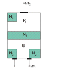
Figure shows the construction of a triac. There are two main terminals namely MT1 and MT2 and the remaining terminal is gate terminal.
There are four different modes of operations, they are-
- When MT2 and Gate being Positive with Respect to MT1
When this happens, current flows through the path P1-N1-P2-N2. Here, P1-N1 and P2-N2 are forward biased but N1-P2 is reverse biased. The triac is said to be operated in positively biased region. Positive gate with respect to MT1 forward biases P2-N2 and breakdown occurs. - When MT2 is Positive but Gate is Negative with Respect to MT1
The current flows through the path P1-N1-P2-N2. But P2-N3 is forward biased and current carriers injected into P2 on the triac. - When MT2 and Gate are Negative with Respect to MT1
Current flows through the path P2-N1-P1-N4. Two junctions P2-N1 and P1-N4 are forward biased but the junction N1-P1 is reverse biased. The triac is said to be in the negatively biased region. - When MT2 is Negative but Gate is Positive with Respect to MT1
P2-N2 is forward biased at that condition. Current carriers are injected so the triac turns on. This mode of operation has a disadvantage that it should not be used for high (di/dt) circuits. Sensitivity of triggering in mode 2 and 3 is high and if marginal triggering capability is required, negative gate pulses should be used. Triggering in mode 1 is more sensitive than mode 2 and mode 3.
Characteristics of a Triac
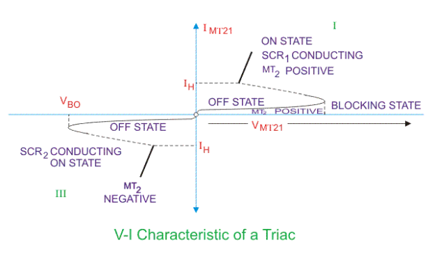
The triac characteristics is similar to SCR but it is applicable to both positive and negative triac voltages. The operation can be summarized as follows-
First Quadrant Operation of Triac
Voltage at terminal MT2 is positive with respect to terminal MT1 and gate voltage is also positive with respect to first terminal.
Second Quadrant Operation of Triac
Voltage at terminal 2 is positive with respect to terminal 1 and gate voltage is negative with respect to terminal 1.
Third Quadrant Operation of Triac
Voltage of terminal 1 is positive with respect to terminal 2 and the gate voltage is negative.
Fourth Quadrant Operation of Triac
Voltage of terminal 2 is negative with respect to terminal 1 and gate voltage is positive.
|
When the device gets turned on, a heavy current flows through it which may damage the device, hence in order to limit the current a current limiting resistor should be connected externally to it. By applying proper gate signal, firing angle of the device may be controlled. The gate triggering circuits should be used for proper gate triggering.
Applications:
- They are used in control circuits.
- It is used in High power lamp switching.
- It is used in AC power control.
UJT :
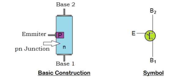
In Unijunction Transistor, the PN Junction is formed by lightly doped N type silicon bar with heavily doped P type material on one side. The ohmic contact on either ends of the silicon bar is termed as Base 1 (B1) and Base 2 (B2) and P-type terminal is named as emitter.
The emitter junction is placed such that it is more close to terminal Base 2 than Base 1. The symbols of both UJT and JFET resemble the same except the emitter arrowhead represents the direction in which conventional current flow, but they operate differently.
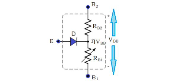
The simplified equivalent circuit as shown in figure shows that N-type channel consists of two resistors RB2 and RB1 in series with an equivalent diode, D representing the PN junction. The emitter PN junction is fixed along the ohmic channel during its manufacturing process.
The variable resistance RB1 is provided between the terminals Emitter (E) and Base 1 (B1), the RB2 between the terminals Emitter (E) and Base 2 (B2). Since the PN junction is more close to B2, the value of RB2 will be less than the variable resistance RB1.
A voltage divider network is formed by the series resistances RB2 and RB1. When a voltage is applied across the semiconductor device, the potential will be in proportion to the position of base points along the channel.
The Emitter (E) will act as input when employed in a circuit, as the terminal B1 will be grounded. The terminal B2 will be positive biased to B1, when a voltage (VBB) applied across the terminals B1 and B2. When the emitter input is zero, the voltage across resistance RB1 of the voltage divider circuit is calculated by
VRB1 = RB1/ RB1 + RB2 * VBB
The important parameter of Unijunction Transistor is ‘intrinsic stand-off ratio’ (η), which is resistive ratio of RB1 to RBB. Most UJT’s have η value ranging from 0.5 to 0.8. The PN junction is reverse biased; when small amount of voltage which is less than voltage developed across resistance RB1 (ηVBB) is applied across the terminal emitter (E).
Thus, high impedance is developed prompting device to move into non-conducting state i.e., it will be switched off and no current flows through it. The UJT begins to conduct when the PN junction is forward biased.
The forward biased is achieved when voltage applied across emitter terminal is increased and becomes more than VRB1. This results in larger flow of emitter current from emitter region to base region. Increase in emitter current reduces the resistance between emitter and Base 1, resulting in negative resistance at emitter terminal.
The Unijunction Transistor (UJT) will act as voltage breakdown device, when the input applied between emitter and base 1 reduces below breakdown value i.e., RB1 increases to a higher value. This shows that RB1 depends on the emitter current and it is variable.
Characteristics Curve of Unijunction Transistor (UJT)
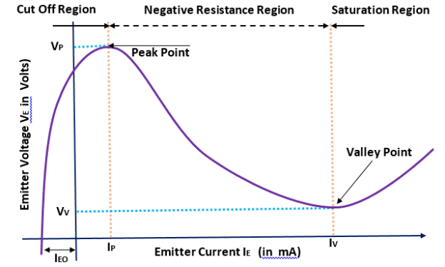
The characteristics of Unijunction Transistor (UJT) can be explained by three parameters:
Cutoff
Cutoff region is the area where the Unijunction Transistor (UJT) doesn’t get sufficient voltage to turn on. The applied voltage hasn’t reached the triggering voltage, thus making transistor to be in off state.
Negative Resistance Region
When the transistor reaches the triggering voltage, VTRIG, Unijunction Transistor (UJT) will turn on. After a certain time, if the applied voltage increases to the emitter lead, it will reach out at VPEAK. The voltage drops from VPEAK to Valley Point even though the current increases (negative resistance).
Saturation
Saturation region is the area where the current and voltage raises, if the applied voltage to emitter terminal increases.
Applications of Unijunction Transistor (UJT)
The Unijunction Transistor can be employed in variety of applications such as:
- Switching Device
- Triggering Device for Triacs and SCR’s
- Timing Circuits
- For phase control
- In sawtooth generators
- In simple relaxation oscillators
Introduction to number system and conversions
A digital system understands positional number system where there are few symbols called digits and this symbol represents different values depending on their position in the number.
A value of the digit is determined by using
- The digit
- Its position
- The base of the number system
Decimal Number System
- Its the system that we use in our daily life. It has a base 10 and uses 10 digits from 0 to 9.
- Here, the successive positions towards the left of the decimal point represent units, tens, hundreds, thousands, and so on.
- Every position represents a specific power of the base (10). For example, the decimal number 4321 consists of the digit 1 in the units position, 2 in the tens position, 3 in the hundreds position, and 4 in the thousands position, and its value can be written as
(1×1000) + (2×100) + (3×10) + (4×l)
(1×10³) + (2×10²) + (3×101) + (4×l00)
1000 + 200 + 30 + 1
1234
- As a computer programmer, we should understand the following number of systems used in computers.
S.N. | Number System & Description |
1 | Binary Number System Base 2. Digits used: 0 and 1 |
2 | Octal Number System Base 8. Digits used: 0 to 7 |
3 | Hexa Decimal Number System Base 16. Digits used: 0 to 9, Letters used: A- F |
De Morgan’s Theorem
(x + y)’ = x’.y’
(x.y)’ = x’ + y’
Simplification of Boolean Functions Numerical
f = p’qr + pq’r + pqr’ + pqr Method 1 Given f = p’qr + pq’r + pqr’ +pqr. In the first and second terms, r is common and in third and fourth terms pq is common. So, taking out the common terms by using Distributive law we get, ⇒ f = (p’q + pq’)r + pq(r’ + r) The terms present in the first parenthesis can be simplified by using the Ex-OR operation. The terms present in the second parenthesis is equal to ‘1’ using Boolean postulate we get ⇒ f = (p ⊕q)r + pq(1) The first term can’t be simplified further. But, the second term is equal to pq using Boolean postulate. ⇒ f = (p ⊕q)r + pq Therefore, the simplified Boolean function is f = (p⊕q)r + pq
Method 2 Given f = p’qr + pq’r + pqr’ + pqr. Using the Boolean postulate, x + x = x. Hence we can write the last term pqr two more times. ⇒ f = p’qr + pq’r + pqr’ + pqr + pqr + pqr Now using the Distributive law for 1st and 4th terms, 2nd and 5th terms, 3rdand 6th terms we get. ⇒ f = qr(p’ + p) + pr(q’ + q) + pq(r’ + r) Using Boolean postulate, x + x’ = 1 and x.1 = x for further simplification . ⇒ f = qr(1) + pr(1) + pq(1) ⇒ f = qr + pr + pq ⇒ f = pq + qr + pr Therefore, the simplified Boolean function is f = pq + qr + pr. Hence we got two different Boolean functions after simplification of the given Boolean function. Functionally, these two functions are the same. As per requirement, we can choose one of them.
Numerical Find the complement of the Boolean function, f = p’q + pq’. Solution: Using DeMorgan’s theorem, (x + y)’ = x’.y’ we get ⇒ f’ = (p’q)’.(pq’)’ Then by second law, (x.y)’ = x’ + y’ we get ⇒ f’ = {(p’)’ + q’}.{p’ + (q’)’} Then by using, (x’)’=x we get ⇒ f’ = {p + q’}.{p’ + q} ⇒ f’ = pp’ + pq + p’q’ + qq’ Using x.x’=0 we get ⇒ f = 0 + pq + p’q’ + 0 ⇒ f = pq + p’q’ Therefore, the complement of Boolean function, p’q + pq’ is pq + p’q’. |
LOGIC GATES
The basic gates are namely AND gate, OR gate & NOT gate.
AND gate
It is a digital circuit that consists of two or more inputs and a single output which is the logical AND of all those inputs. It is represented with the symbol ‘.’.
The following is the truth table of 2-input AND gate.
A | B | Y = A.B |
0 | 0 | 0 |
0 | 1 | 0 |
1 | 0 | 0 |
1 | 1 | 1 |
Here A, B are the inputs and Y is the output of two-input AND gate.
If both inputs are ‘1’, then only the output, Y is ‘1’. For the remaining combinations of inputs, the output, Y is ‘0’.
The figure below shows the symbol of an AND gate, which is having two inputs A, B, and one output, Y.
Fig. : AND gate (ref. 1) |
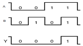
Timing Diagram:
|
OR gate
It is a digital circuit that has two or more inputs and a single output which is the logical OR of all those inputs. It is represented with the symbol ‘+’.
The truth table of the 2-input OR gate is:
A | B | Y = A + B |
0 | 0 | 0 |
0 | 1 | 1 |
1 | 0 | 1 |
1 | 1 | 1 |
Here A, B are the inputs and Y is the output of two-input OR gate.
When both inputs are ‘0’, then only the output, Y is ‘0’. For remaining combinations of inputs, the output, Y is ‘1’.
The figure below shows the symbol of an OR gate, which is having two inputs A, B, and one output, Y.
Fig. : OR gate (ref. 1) |
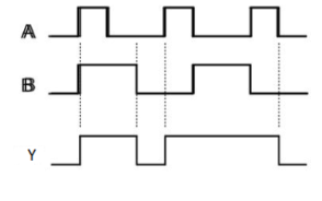
Timing Diagram:
|
NOT gate
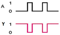
It is a digital circuit that has one input and one output. Here the output is the logical inversion of input. Hence, it is also called an inverter.
The truth table of NOT gate is:
A | Y = A’ |
0 | 1 |
1 | 0 |
Here A and Y are the corresponding input and output of a NOT gate. When A is ‘0’, then, Y is ‘1’. Similarly, when, A is ‘1’, then, Y is ‘0’.
The figure below shows the symbol of NOT gate, which has one input, A and one output, Y.

Fig. : NOT gate (ref. 1)
Timing Diagram:
Universal gates
- NAND & NOR gates are known as universal gates.
- We can implement any Boolean function by using NAND gates and NOR gates alone.
NAND gate
It is a digital circuit that has two or more inputs and single output and it is the inversion of logical AND gate.
The truth table of the 2-input NAND gate is:
A | B | Y = (A.B)’ |
0 | 0 | 1 |
0 | 1 | 1 |
1 | 0 | 1 |
1 | 1 | 0 |
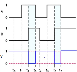
Here A, B are the inputs and Y is the output of two-input NAND gate. When both inputs are ‘1’, then the output, Y is ‘0’. If at least one of the input is zero, then the output, Y is ‘1’. This is just the inverse of AND operation.
The image shows the symbol of NAND gate:

Fig.: NAND gate (ref. 1)
NAND gate works the same as AND gate followed by an inverter.
Timing Diagram:
NOR gate
It is a digital circuit that has two or more inputs and a single output which is the inversion of logical OR of all inputs.
The truth table of 2-input NOR gate is:
A | B | Y = (A+B)’ |
0 | 0 | 1 |
0 | 1 | 0 |
1 | 0 | 0 |
1 | 1 | 0 |
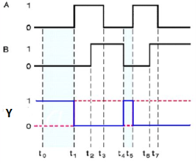
Here A and B are the two inputs and Y is the output. If both inputs are ‘0’, then the output is ‘1’. If anyone of the input is ‘1’, then the output is ‘0’. This is exactly opposite to the two-input OR gate operation.
The symbol of NOR gate is:

Fig.: NOR gate (ref. 1)
NOR gate works the same as that of OR gate followed by an inverter.
Timing Diagram:
Special Gates
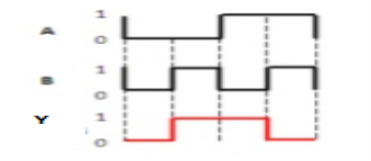
Ex-OR gate
It stands for the Exclusive-OR gate. Its function varies when the inputs have an even number of ones.
The truth table of the 2-input Ex-OR gate is:
A | B | Y = A⊕B |
0 | 0 | 0 |
0 | 1 | 1 |
1 | 0 | 1 |
1 | 1 | 0 |
Here A, B are the inputs and Y is the output of two input Ex-OR gate. The output (Y) is zero instead of one when both the inputs are one.
Therefore, the output of the Ex-OR gate is ‘1’, when only one of the two inputs is ‘1’. And it is zero when both inputs are the same.
The symbol of the Ex-OR gate is as follows:

Fig.: XOR gate (ref. 1)
It is similar to that of the OR gate with an exception for a few combinations (s) of inputs. Hence, the output is also known as an odd function.
Timing Diagram:
Ex-NOR gate
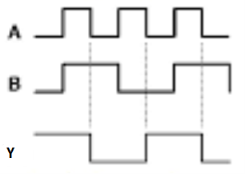
It stands for the Exclusive-NOR gate. Its function is the same as that of the NOR gate except when the inputs having an even number of ones.
The truth table of the 2-input Ex-NOR gate is:
A | B | Y = A⊙B |
0 | 0 | 1 |
0 | 1 | 0 |
1 | 0 | 0 |
1 | 1 | 1 |
Here A, B are the inputs and Y is the output. It is the same as the Ex-NOR gate with the only modification in the fourth row. The output is 1 instead of 0 when both the inputs are one.
Hence the output of the Ex-NOR gate is ‘1’ when both inputs are the same and 0 when both the inputs are different.
The symbol of the Ex-NOR gate is:

Fig.: XNOR gate (ref. 1)
It is similar to the NOR gate except for a few combinations (s) of inputs. Here the output is ‘1’ when even the number of 1 is present at the inputs. Hence is also called an even function.
Timing Diagram:
Different types of insulated wires primarily used for house wiring are
1. Vulcanised Indian Rubber Insulated Wires:
On the conductor one or more layers of vulcanised Indian Rubber (V.I.R.) i.e., rubber treated with sulphur at high temperature, is applied. For removing the bad effect of sulphur on copper or aluminium, the conductor is thoroughly tinned or a layer of pure rubber is applied on the conductor.
Finally the rubber insulation is covered either by cotton tape impregnated with moisture resisting compound like bitumen or wax, or covered with cotton tape. V.I.R. wires are single-core type and usually used in conduit wiring, wood casing and cleat wiring, etc. In recent years, however, single-core P.V.C. wires have largely replaced V.I.R. wires.
2. Tough Rubber Sheathed (T.R.S.) and Cab Tyre Sheathed (C.T.S.) Wires:
Over the tinned copper or aluminium conductor a layer of pure rubber or rubber treated with sulphur is used. As outer protective layer tough rubber sheath (T.R.S.) wires and cab tyre sheath (C.T.S.) wires are provided. These may be used in damp places or in open atmosphere. T.R.S. or C.T.S. wires are light in weight and cheaper in cost.
These wires are available in single-cores twin-core, three-core conductor. Single-core and twin-core wires are mainly used in house wiring, and twin-core and three core wires are used for giving supply to cranes, hoists, etc. and also for drawing service connections from the overhead distribution lines or from one building to another.
The rubber insulation over each conductor has different colours for different cores. In recent years for service connections and house wiring P.V.C. wires are preferred over T.R.S. or C.T.S. wires.
3. Metal Sheathed or Lead Sheathed Wires:
In these wires V.I.R. types are provided with a continuous lead sheath covering which is mechanically strong and moisture proof. Due to its high cost compared to C.T.S. wires, lead sheathed wires are not used for internal wiring but used for service connections and for wiring under abnormal climatic conditions with high moisture.
Lead sheathed cables are available in many forms like single-core, twin-core flat, three-core flat and twin-core flat with an earth continuity conductor. In this type also rubber insulations over the conductor have different colours for different cores.
4. Weather-Proof Wires:
Weather-proof wire is mainly used in outdoor work where the wire remains exposed to open atmosphere. These wires are of V.I.R. insulated type suitably taped, braided and compounded with weather-resisting material. The conductor is of tinned copper or aluminium over which a layer of rubber treated with sulphur is applied. Weather-proof cables are useful is industries and in outdoor wiring at low and medium voltages.
5. Wires with Thermo-Plastic Insulation (P.V.C. Wires):
Here conductor is insulated with poly-vinyl chloride (P.V.C.), a thermo-plastic material. This type of insulation is not affected by acid, alkali, ozone, humidity or the sun rays. Rubber insulation is deteriorated shortly but P.V.C. remains unaffected as it is much harder than rubber. So additional protection like cotton tapping or cotton braiding is not required against mechanical injury. It is inflammable but when the source of flame is removed, it stops burning.
Hence proves that P.V.C. insulation does not help combustion. However, it becomes semi-melted when excessively heated and becomes brittle under extreme cold condition. For that reason P.V.C. wires cannot be used for giving connections to the heating appliances. It is also not to be used for wiring in a place exposed to weather particularly where there is frequent snowfall.
Concept of fuses:
- The principle of a fuse is based on the heating effect of the electric current. A simple fuse consists of a small conductive material with low resistance and it is placed in series with the circuit.
- The cross section area of this conducting material is designed such that it allows a certain amount of current that is permitted to flow in the circuit.
- When the current in the circuit exceeds this permitted value (which may be caused due to overload, short circuit or load mismatch), this excessive current will melt the conductive element in the fuse and opens the circuit.
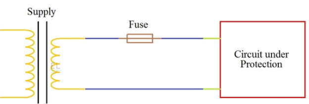
- This will disconnect the power supply and thus, the rest of the circuit is protected from being damaged. The following image shows a block diagram of how a fuse is connected in the circuit.
|
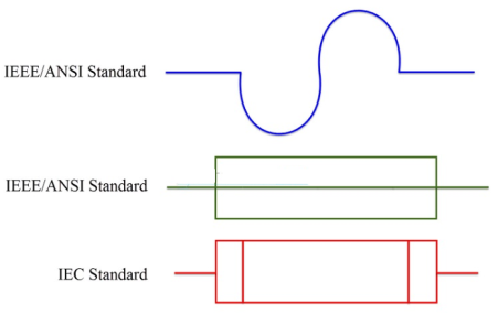
Fuses are very simple and cheap devices that are being used for over hundred years as a protective equipment. For electrical drawings and circuits, there are three symbols of fuses we can use. The following image shows the symbols of fuse along with their standards.
|
- Wiring installation
The MCB, MCCB, ELCB, RCCB and RCD are all protective gadgets designed for protecting electrical systems, circuit wiring, equipment, human life, and property from various faults occurring in the electrical system and should be installed as per the type of protection required besides selecting the correct rating of these protection gadgets to disconnect the electrical supply from the electrical system and provide requisite protection.
- Concept of earthing
The process of transferring the immediate discharge of the electrical energy directly to the earth by the help of the low resistance wire is known as the electrical earthing. The electrical earthing is done by connecting the non-current carrying part of the equipment or neutral of supply system to the ground.
Electrical Earthing
The process of transferring the immediate discharge of the electrical energy directly to the earth by the help of the low resistance wire is known as the electrical earthing. The electrical earthing is done by connecting the non-current carrying part of the equipment or neutral of supply system to the ground.
Mostly, the galvanised iron is used for the earthing. The earthing provides the simple path to the leakage current. The shortcircuit current of the equipment passes to the earth which has zero potential. Thus, protects the system and equipment from damage.
- Energy bill calculations
Suppose, a consumer consumes 1000 watts load per hour daily for one month. Calculate The Total Energy bill of the consumer if per unit rate is 9 (In $, £, €, INR ,Rs, DHR, Riyal etc) [Take 1 month = 30 Days].
Solution:
1unit = 1kWh.
So Total kWh = 1000 Watts x 24 Hrs x 30 Days = 720000 watts/hour.
we Want to convert it into Units, Where is 1unit = 1kWh.
So total Consumed units. 720000/1000…… (k=kilo=1000).
Total Units = 720.
Cost of per unit is 9.
So total Cost or Electricity bill= 720 x 9 = 6480.
Reference Books:
1. V. N. Mittal, Arvind Mittal, ‘Basic Electrical Engineering’, Tata McGraw Hill publishing co. ltd, New Delhi.
2. D. P. Kothari, I.J Nagrath, ‘Basic Electrical Engineering’, Tata McGraw Hill
3. M. S. Naidu, S. Kamakshaiah, ‘Introduction to Electrical Engineering’, Tata McGraw Hill.
4. P. Tiwari, ‘Basic Electrical Engineering’, New Age Publication.
5. Vincent Del Toro, ‘Electrical Engineering Fundamentals’, Pearson
6. R. P. Jain, ‘Modern Digital Electronics’ McGraw Hill Education (India) Private Limited, Fourth Edition, 2017.
7. B. L. Theraja, ‘Applied Electronics’ S. Chand Publication
8. A.P. Malvino, ‘Electronics Principles’ TMH Publications.
