UNIT - 3
Semiconductors and Light-Semiconductor Interactions
Semiconductors
Semiconductors are materials that have conductivity between conductors and insulators.
Semiconductors can be pure elements, such as silicon or germanium, or compounds such as gallium arsenide or cadmium selenide.
They are not good conductors nor good insulators as their name “semi”-conductors.
These materials such as silicon (Si), germanium (Ge), and gallium arsenide (GaAs), have electrical properties somewhere in the middle, between those of a “conductor” and an “insulator”.
They have very few “free electrons” because their atoms are closely grouped in a crystalline pattern called a “crystal lattice” but electrons are still able to flow, but only under special conditions.
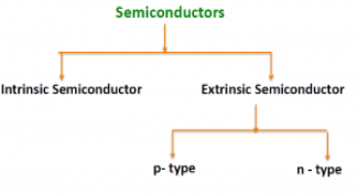
There are two basic groups or classifications that can be used to define the different semiconductor types:
- Intrinsic Semiconductor
- Extrinsic Semiconductor
|
Figure 1: Type of semiconductor
The semiconductor is divided into two types. One is an Intrinsic Semiconductor and the other is an Extrinsic semiconductor. The pure form of the semiconductor is known as the intrinsic semiconductor and the semiconductor in which intentional impurities are added for making it conductive is known as the extrinsic semiconductor.
The conductivity of the intrinsic semiconductor becomes zero at room temperature while the extrinsic semiconductor is very little conductive at room temperature. The detailed explanation of the two types of the semiconductor is given below.
INTRINSIC SEMICONDUCTOR
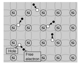
An intrinsic type of semiconductor material made to be very pure chemically. As a result, it possesses a very low conductivity level having very few charge carriers, namely holes and electrons, which it possesses in equal quantities.
|
Figure 2: Intrinsic Semiconductor
The most commonly used semiconductor basics material by far is silicon. Silicon has four valence electrons in its outermost shell which it shares with its neighbouring silicon atoms to form a full orbital of eight electrons. The structure of the bond between the two silicon atoms is such that each atom shares one electron with its neighbour making the bond very stable.
As there are very few free electrons available to move around the silicon crystal, crystals of pure silicon (or germanium) are therefore good insulators. Silicon atoms are arranged in a definite symmetrical pattern making them a crystalline solid structure. A crystal of pure silica (silicon dioxide or glass) is generally said to be an intrinsic crystal (it has no impurities) and therefore has no free electrons.
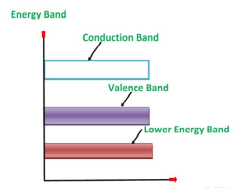
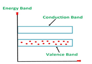
An extremely pure semiconductor is called an Intrinsic Semiconductor. Based on the energy band phenomenon, an intrinsic semiconductor at absolute zero temperature is shown below.
|
Figure 3: Intrinsic semiconductor at absolute zero temperature.
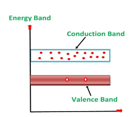
Its valence band is filled and the conduction band is empty. When the temperature is raised and some heat energy is supplied to it, some of the valence electrons are lifted to the conduction band leaving behind holes in the valence band as shown below.
|
Figure 4: Intrinsic semiconductor at T >0
A hole is the absence of an electron in a particular place in an atom. Although it is not a physical particle in the same sense as an electron, a hole can be passed from atom to atom in a semiconductor material. It is considered to have a positive charge. Holes are positive charge carriers.
The electrons reaching the conduction band move randomly. The holes created in the crystal also free to move anywhere.
This behaviour of the semiconductor shows that they have a negative temperature coefficient of resistance. This means that with the increase in temperature, the resistivity of the material decreases, and the conductivity increases.
But simply connecting a silicon crystal to a battery supply is not enough to extract an electric current from it. To do that we need to create a “positive” and a “negative” pole within the silicon allowing electrons and therefore electric current to flow out of the silicon. These poles are created by doping the silicon with certain impurities.
DOPING
The process by which an impurity is added to a semiconductor is known as Doping. The amount and type of impurity which is to be added to the material have to be closely controlled during the preparation of extrinsic semiconductor. Generally, one impurity atom is added to 108 atoms of a semiconductor.
The purpose of adding impurity in the semiconductor crystal is to increase the number of free electrons or holes to make it conductive.
If a Pentavalent impurity, having five valence electrons is added to a pure semiconductor a large number of free electrons will exist. Which makes an n-type extrinsic semiconductor.
If a trivalent impurity having three valence electrons is added, a large number of holes will exist in the semiconductor. Which makes a p-type extrinsic semiconductor.
EXTRINSIC SEMICONDUCTOR
Extrinsic types of semiconductors are those where a small amount of impurity has been added to the basic intrinsic material. This 'doping' uses an element from a different periodic table group and in this way, it will either have more or fewer electrons in the valence band than the semiconductor itself. This creates either an excess or shortage of electrons. In this way two types of semiconductors are available: Electrons are negatively charged carriers. Holes are positively charged carriers.
Depending upon the type of impurity added the extrinsic semiconductor may be classified as an n-type semiconductor and p-type semiconductor.
P-TYPE EXTRINSIC SEMICONDUCTOR
The extrinsic p-Type Semiconductor is formed when a trivalent impurity is added to a pure semiconductor in a small amount, and as a result, a large number of holes are created in it. A large number of holes are provided in the semiconductor material by the addition of trivalent impurities like Gallium and Indium. Such type of impurities which produce a p-type semiconductor is known as an Acceptor Impurities because each atom of them creates one hole which can accept one electron.
In a P-type semiconductor material, there is a shortage of electrons, i.e. there are 'holes' in the crystal lattice. Electrons may move from one empty position to another and in this case, it can be considered that the holes are moving. This can happen under the influence of a potential difference and the holes can be seen to flow in one direction resulting in an electric current flow. It is harder for holes to move than for free electrons to move and therefore the mobility of holes is less than that of free electrons. Holes are positively charged carriers.
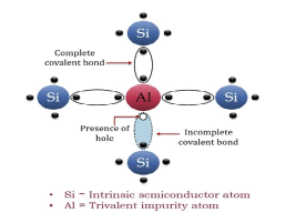
A trivalent impurity like Aluminium, having three valence electrons is added to Silicon crystal in a small amount. Each atom of the impurity fits in the Silicon crystal in such a way that its three valence electrons form covalent bonds with the three surrounding Silicon atoms as shown in the figure below.
|
Figure 5: p-Type Semiconductor
ENERGY BAND DIAGRAM OF P-TYPE SEMICONDUCTOR
The energy band diagram of a p-Type Semiconductor is shown below.
|
Figure 6: Energy band diagram of a p-Type Semiconductor
A large number of holes or vacant space in the covalent bond is created in the crystal with the addition of the trivalent impurity. A small or minute quantity of free electrons is also available in the conduction band.
They are produced when thermal energy at room temperature is imparted to the Silicon crystal-forming electron-hole pairs. But the holes are more in number as compared to the electrons in the conduction band. It is because of the predominance of holes over electrons that the material is called a p-type semiconductor. The word “p” stands for positive material.
CONDUCTION THROUGH P TYPE SEMICONDUCTOR
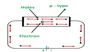
In p-type semiconductors, a large number of holes are created by the trivalent impurity. When a potential difference is applied across this type of semiconductors.
Figure 7: Conduction through p type semiconductor
The holes are available in the valence band are directed towards the negative terminal. As the current flow through the crystal is by holes, which are a carrier of positive charge, therefore, this type of conductivity is known as positive or p-type conductivity. In a p-type conductivity, the valence electrons move from one covalent to another.
The conductivity of an n-type semiconductor is nearly double that of a p-type semiconductor. The electrons available in the conduction band of the n-type semiconductor are much more movable than holes available in the valence band in a p-type semiconductor. The mobility of holes is poor as they are more bound to the nucleus.
Even at room temperature, the electron-hole pairs are formed. These free electrons which are available in minute quantity also carry a little amount of current in the p-type semiconductors.
N-TYPE EXTRINSIC SEMICONDUCTOR
When a few Pentavalent impurities such as Phosphorus whose atomic number is 15, which is categorized as 2, 8, and 5. It has five valence electrons, which are added to silicon crystals. Each atom of the impurity fits in four silicon atoms as shown in the figure below.
Hence, each Arsenic atom provides one free electron in Silicon crystal. Since an extremely small amount of Phosphorus, impurity has a large number of atoms; it provides millions of free electrons for conduction.
|
Figure 8: N-type semiconductor
An N-type semiconductor material has an excess of electrons. In this way, free electrons are available within the lattices, and their overall movement in one direction under the influence of a potential difference results in an electric current flow. This is an N-type semiconductor, the charge carriers are electrons.
ENERGY DIAGRAM OF N-TYPE SEMICONDUCTOR
A large number of free electrons are available in the conduction band because of the addition of the Pentavalent impurity. These electrons are free electrons that did not fit in the covalent bonds of the crystal. However, a minute quantity of free electrons is available in the conduction band forming hole- electron pairs.
The Energy diagram of the n-type semiconductor is shown in the figure below.
|
Figure 9: Energy diagram of the n-type semiconductor
- The addition of pentavalent impurity results in a large number of free electrons.
- When thermal energy at room temperature is imparted to the semiconductor, a hole-electron pair is generated and as a result, a minute quantity of free electrons is available. These electrons leave behind holes in the valence band.
- Here n stands for negative material as the number of free electrons provided by the pentavalent impurity is greater than the number of holes.
CONDUCTION THROUGH N-TYPE SEMICONDUCTOR
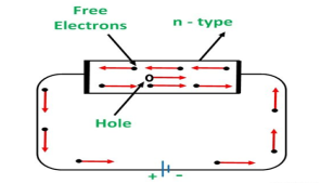
In the n-type semiconductor, a large number of free electrons are available in the conduction bands which are donated by the impurity atoms. The figure below shows the conduction process of an n-type semiconductor.
When a potential difference is applied across this type of semiconductor, the free electrons are directed towards the positive terminals. It carries an electric current. As the flow of current through the crystal is constituted by free electrons which are carriers of a negative charge, therefore, this type of conductivity is known as negative or n-type conductivity.
Figure 10: Conduction through n-type semiconductor
The electron-hole pairs are formed at room temperature. These holes which are available in small quantities in the valence band also consist of a small amount of current. For practical purposes, this current is neglected.
Key Takeaways
- Semiconductors are materials that have conductivity between conductors and insulators.
- The semiconductor is divided into two types. One is an Intrinsic Semiconductor and the other is an Extrinsic semiconductor.
- The pure form of the semiconductor is known as the intrinsic semiconductor
- The semiconductor in which intentional impurities are added for making it conductive is known as the extrinsic semiconductor.
- A hole is the absence of an electron in a particular place in an atom.
- The process by which an impurity is added to a semiconductor is known as Doping.
- Depending upon the type of impurity added the extrinsic semiconductor may be classified as an n-type semiconductor and p-type semiconductor.
- The extrinsic p-Type Semiconductor is formed when a trivalent impurity is added to a pure semiconductor in a small amount, and as a result, a large number of holes are created in it.
- The extrinsic n-Type Semiconductor is formed when a Pentavalent impurity is added to a pure semiconductor in a small amount, and as a result, a large number of electrons are created in it.
FERMI ENERGY
Intrinsic semiconductors—carrier concentration
Here we will calculate the number of electrons excited into the conduction band at temperature T and also the hole concentration in the valence band. It is assumed that the electrons in the conduction band behave as if they are free particles with effective mass me* and the holes near the top of the valence band behave as if they are free particles with effective mass mh*.
Here we will calculate the electron concentration, hole concentration
The density of Electrons in Conduction Band
The number of free electrons per unit volume of a semiconductor having energies in between E and E + dE is represented as N(E) dE
dE = width of Energy band
Therefore, we have:
N(E) dE = ge(E) dE fe(E) ……….(1) |
ge(E) = The density of electron states per unit volume
fe(E) = Fermi-Dirac distribution function i.e. probability that an electron occupies an electron state
The number of electrons present in the conduction band per unit volume of material ‘n’ is obtained by integrating N(E) dE between the limits Ec and Ect
Where Ec = the bottom energy levels of the conduction band
Ect = the bottom and top energy levels of the conduction band
n = |
can be written as
n = n = |
we know that above Ect, there are no electrons.
Hence, Equation (3) becomes
n = n = |
The Fermi-Dirac distribution function fe(E) can be represented as:
|
Compared to the exponential value, so the ‘1’ in the denominator can be neglected.
So Hence, |
The density of electron states ge(E) in the energy space from E = 0 to E can be written as:
|
where me* is the effective mass of an electron and h is Planck’s constant.
|
To evaluate n, the density of states is counted from Ec, since the minimum energy state in the conduction band is Ec. so eq (8) can become
|
Substituting Equations (6) and (9) in (4) gives
n = n = |
The above equation can be simplified by the following substitution:
Put ɛ = E − Ec ………… (11) So, dɛ = dE |
In Equation (11), Ec is constant, as we change the variable E to ε in Equation (10), the integral limits also change.
In Equation (11), as E → Ec then ε → 0 and E → ∞, then ε also → ∞. |
the exponential term in Equation (10) becomes:
|
Substituting Equations (11) and (12) in (10), we get:
n = n = |
Above integral (I) can be simplified by substitution.
Put ε = x2
so that dɛ = 2x dx I = = = |
Substituting Equation (14) in (13) gives:
n = n = n = n = |
The term  is almost a constant compared with the exponential term as the temperature changes. So, it is a pseudo constant and is given by the symbol Nc. So, we have
n =Nc |
The density of Holes in Valence Band
The number of holes per unit volume of semiconductor in the energy range E and E + dE in the valence band is represented as P(E) dE. Proceeding the same way (as in the case of electrons) we have
Therefore, we have:
P(E) dE = gh(E) dE fh(E) ……….(17) dE = width of Energy band gh(E) = The density of holes states per unit volume fh(E) = Fermi-Dirac distribution function i.e. probability that a hole occupies an electron state |
The number of electrons present in the conduction band per unit volume of material ‘n’ is obtained by integrating P(E) dE between the limits Evb and EV
where EV = the bottom energy levels of the valence band
Evb = the bottom and top energy levels of the valence band
The total number of holes present in the valence band per unit volume of material ‘p’ is obtained by integrating P(E) dE
|
Equation (18) can be represented as:
|
Now we know that below Evb no holes are present. Hence, Equation (19) becomes
|
We know a hole can also be defined as the absence of an electron.
presence of a hole = the absence of an electron
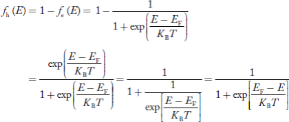
Hence, the Fermi-Dirac function of holes fh(E) in the valence band is:
|
Compared to exponential, the ‘1’ in the denominator is negligible,
|
Hence,
|
The density of hole states between E and E + dE in valence band can be written similar to Equation (8.9) for electrons.
|
Where mh* is the effective mass of the hole.
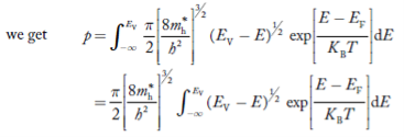
Substituting Equations (21) and (22) in (20),
|
The above equation can be simplified by the substitution:
Put ɛ = EV − E ............. (24) |
so dɛ = − dE |
In Equation (24), EV is constant, as we change the variable E to ε in Equation (23), the integral limits also change.
In Equation (24),
as E → EV then ε → 0 and E→ −∞, then ε → ∞ |
the exponential term in Equation (23) becomes:
|
Substituting Equations (24) and (25) in (23), we get:
|
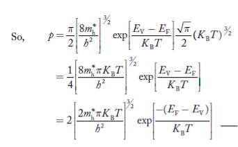
From Equation (14), we know the integral value  T)3/2 put here and we get
|
The term  is almost constant compared with the exponential term as the temperature changes. So, it is a pseudo constant and is given by the symbol NV. So, we have
|
Fermi Level
We know that in an intrinsic semiconductor
Electron concentration ‘n’ = Hole concentration ‘p’
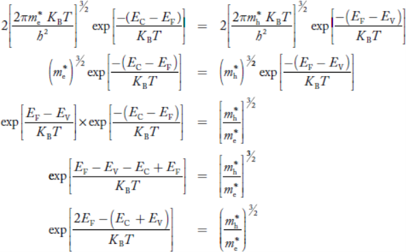
Equating Equations (15) and (27), we get
|
Taking logarithms on both sides, we get
|
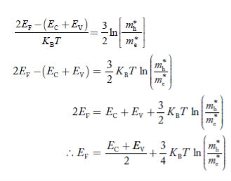
Normally, mh* is greater than me*, since ln  is very small so that EF is just lie in the middle of the energy gap
Temperature effect on Fermi level
Fermi level slightly rises with an increase of temperature.
But in the case of a pure intrinsic semiconductor like Si and Ge,
mh* ≈ me*
So in these cases, the Fermi level lies in the middle of the energy gap.
DEPENDENCE OF FERMI ENERGY ON CARRIER CONCENTRATION AND TEMPERATURE (QUALITATIVE)-
Carrier Concentration in Extrinsic Semiconductors
The number of charge carriers presents per unit volume of a semiconductor material is called carrier concentration.
Suppose donor and acceptor atoms are doped in a semiconductor.
At temperature T K,
n = number of conduction electrons
p = number of holes
N−A = number of acceptor ions
N+D = number of donor ions
We know that the below equation holds good in the semiconductor. The total negative charge due to conduction electrons and acceptor ions is equal to holes and donor ions in a unit volume of material.
So the material will be considered neutral if,
n + N−A = p + N+D ……….(34)
Equation (34) is called the charge neutrality equation.
In the above equation
|
Concentration of acceptor ions N−A = acceptor concentration x probability of finding an electron in acceptor level
|
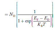
Similarly, the donor ions concentration is
|
|
In n-type material
Note
nn represents electrons in n-type material
pn represents holes concentration in n-type material.
there are no acceptor atoms so N−A = 0.
At 0 K, all the electron states at the donor level are occupied by electrons.
As the temperature is increased from 0 K, some of the electrons jump from these donor states into the conduction band.
Also, the concentration of holes is extremely less compared with the concentration of conduction electrons [p << n]
From Equation (34) we have
n = p N+D (Or) n ≈ N+D …………(38) [since p << N+D] |
At temperature T K,
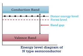
As the temperature increase, almost all the donor atoms donate electrons to the conduction band.
|
Figure 11: Energy level diagram of N type semiconductor
So, in n-type material, the free electron concentration is almost equal to the donor atoms.
So we can rewrite the above equation as
nn ≈ ND …………….(39) |
where nn represents electrons in n-type material
also, the hole concentration in n-type material can be obtained by applying the law of mass action nn pn =ni2
|
where pn represents holes concentration in n-type material.
In n-type material at 0 K, the Fermi energy level lies in the middle of Ec and ED
|
At temperature> 0K
|
With the increase in temperature, the Fermi level shifts upwards according to Equation (61) slightly due to the ionization of donor atoms.
With further increase of temperature, electron-hole pairs are generated due to the breaking of covalent bonds, hence Fermi level shifts downwards.
In p-type semiconductor
Note
pp represents holes in the p-type material
np represents electrons in the p-type material
There are no donor atoms so means no ions present  = 0.
= 0.
At 0 K, all the acceptor levels are not occupied by electrons.
As the temperature is increased from 0 K, some electrons jump from top valence band energy levels to the acceptor states, leaving holes in the valence band and acceptor ions  are formed.
At some room temperature T K, the concentration of conduction electrons is extremely less compared with hole concentration.
∴ From Equation (34), we have
n + N−A = p ……………(42) (or) N−A ≈ p ……………. (43) [since n << N−A] |
At temperature T K, in p-type material,
the hole concentration is almost equal to the acceptor atoms in a unit volume of the material.
So, Equation (43) can be written as
pp ≈ NA ……………….(44) |
where pp represents holes in the p-type material
The electron concentration in p-type material can be obtained by applying the law of mass action as nppp = ni2
|
where np represents free electron concentration in the p-type material.
|
Figure 12: Energy level diagram of N type semiconductor.
In p-type material, the Fermi level lies in between EV and EA at 0 K
|
As the temperature is increased from 0 K, the Fermi level shifts downwards slightly as per Equation (46) due to ionization of acceptor atoms.
And with a further increase of temperature, electron-hole pairs are generated due to the breaking of covalent bonds, so the Fermi level shifts upwards.
Key Takeaways
- The density of Electrons in Conduction Band
- n =Nc

- n =Nc
- The density of Holes in Valence Band
|
3. Fermi level slightly rises with an increase of temperature. But in the case of a pure intrinsic semiconductor like Si and Ge, mh* ≈ me*, So in these cases, the Fermi level lies in the middle of the energy gap.
4. Carrier Concentration in Extrinsic Semiconductors
5. The donor ions concentration is
|
6. Concentration of acceptor ions N−A
|
7. Fermi Level shifts in case of extrinsic semiconductor.
Carrier generation is a process where electron-hole pairs are created by exciting an electron from the valence band of the semiconductor to the conduction band, thereby creating a hole in the valence band.
Recombination is the reverse process where electrons from the conduction and holes from valence band recombine and are annihilated.
These processes must conserve both quantized energy and momentum, and the vibrating lattice plays a large role in conserving momentum.
- Recombination and generation are always happening in semiconductors both optically and thermally.
- Their rates are in balance at equilibrium.
- If the product of the rate becomes greater than the recombination rate, again driving the system back towards equilibrium.
- As the electron and hole densities is a constant at equilibrium, maintained by recombination and generation occurring at equal rates.
- When there is a surplus of carriers the rate of recombination becomes greater than the rate of generation, driving the system back towards equilibrium.
In semiconductors several different processes exist which lead to recombination, the most important ones are:
1) Band-to-band recombination
2) Auger generation/recombination
3) Surface recombination
1) Band-to-band recombination or Radiative recombination
Band-to-band recombination or Radiative recombination is the reverse process of photon absorption, where an electron drops back down to its equilibrium energy band and radiates a photon.
It is the process of electrons jumping down from the conduction band to the valence band in a radiative manner.
During band-to-band recombination the energy absorbed by a material is released in the form of photons. Generally, these released photons contain the same or less energy than those initially absorbed.
The photon emitted may have the energy of the band gap difference or less, depending on how much energy is lost in the mechanism
Radiative recombination plays a more major role in direct band semiconductors.
The total radiative recombination rate, given below as R, is proportional to the product of the concentration of occupied states (electrons, n) in the conduction band and that of the unoccupied states in the valence band (holes, p)
R= Bnp |
Band-to-band recombination depends on the density of available electrons and holes. Both carrier types need to be available in the recombination process. Therefore, the rate is expected to be proportional to the product of n and p. Also, in thermal equilibrium, the recombination rate must equal the generation rate since there is no net recombination or generation. As the product of n and p equals ni2 in thermal equilibrium, the net recombination rate can be expressed as:
U= B(np-ni2) |
where B is the bimolecular recombination constant for a given semiconductor. It can be calculated from the semiconductor’s absorption coefficient. ni2 is the familiar “intrinsic carrier concentration”
2. Auger recombination Auger recombination involves three particles: an electron and a hole, which recombine in a band-to-band transition and give off the resulting energy to another electron or hole. The expression for the net recombination rate is therefore similar to that of band-to-band recombination but includes the density of the electrons or holes, which receive the released energy from the electron-hole annihilation.
In other words Auger recombination the energy is given to a third carrier which is excited to a higher energy level without moving to another energy band.
After the interaction, the third carrier normally loses its excess energy to thermal vibrations. Since this process is a three-particle interaction, it is normally only significant in non-equilibrium conditions when the carrier density is very high.
Auger recombination is most important at high carrier concentrations caused by heavy doping. In silicon-based solar cells, Auger recombination limits the lifetime and ultimate efficiency.
The more heavily doped the material is, the shorter the Auger recombination lifetime.
3. Surface recombination
Recombination at surfaces and interfaces can have a significant impact on the behavior of semiconductor devices.
Areas of defect, such as at the surface of solar cells where the lattice is disordered, recombination is very high.
This is because surfaces and interfaces typically contain a large number of recombination centers because of the abrupt termination of the semiconductor crystal, which leaves a large number of electrically active states.
In addition, the surfaces and interfaces are more likely to contain impurities since they are exposed during the device fabrication process.
The net recombination rate due to trap-assisted recombination and generation is given by:
|
the recombination is due to a two-dimensional density of traps, Nts, as the traps only exist at the surface or interface.
Understanding the impacts and the ways to limit surface recombination leads to better and more robust solar cell designs. Surface recombination is high in solar cells, but can be limited.
Key Takeaways
- Carrier generation is a process where electron-hole pairs are created by exciting an electron from the valence band of the semiconductor to the conduction band, thereby creating a hole in the valence band.
- Recombination is the reverse process where electrons from the conduction and holes from valence band recombine and are annihilated.
- These processes must conserve both quantized energy and momentum, and the vibrating lattice plays a large role in conserving momentum.
- Recombination and generation are always happening in semiconductors both optically and thermally. Their rates are in balance at equilibrium.
- In semiconductors several different processes exist which lead to recombination, the most important ones are: Band-to-band recombination, Auger generation/recombination and Surface recombination
Drift current and diffusion currents
In case of semiconductors we observe two kinds of currents.
Drift current
Diffusion current
Drift current Definition: The flow of electric current due to the motion of charge carriers under the influence of external electric field is called drift current.
When an electric field E is applied across a semiconductor material, the charge carriers attain a drift velocity vd
So drift velocity vd =μ .E |
The relation between current density J and drift velocity vd is
J = Nqvd |
Where N is the carrier concentration
q is the charge of electron or hole
From equations (1) and (2), we get
Jdrift = Nq μE |
μ is the mobility of charge carrier.
The above equation shows the general expression for drift current density. Drift current density due to electrons is
Je(drift) = neμeE |
Where n is the electrons carrier concentration
and μe is the mobility of electrons.
Drift current density due to holes is
Jh(drift) = peμhE |
Where p is the carrier concentration of holes.
μh is the mobility of holes
so Total drift current density
Jdrift (total) = Je(drift) + Jh(drift) = neμeE + peμhE = eE (nμe+pμh ) |
Diffusion current
Definition: The flow of electric current due to the motion of charge carriers under concentration gradient is called diffusion current
Or
The motion of charge carriers from the region of higher concentration to lower concentration leads to a current called diffusion current.
Let ∆N be the excess electron concentration. Then according to Fick’s law, the rate of diffusion of charge carriers is proportional to concentration gradient
Rate of diffusion of charge ∝ - = - D |
Where D is the diffusion coefficient of charge carriers.
The negative sign indicates decrease of N with increase of x So,
the diffusion current density Jdiffu is
Jdiffu = - qD |
Where q is the charge of the charge carrier
Diffusion current density due to holes is
Jdiffu (hole) = - eDh |
Diffusion current density due to electrons is (as electron carry negative charge so we will get +sign here.
Jdiffu (electrons) = eDe Jdiffu (total) = Jdiffu (hole) + Jdiffu (electrons) Jdiffu (total) = - eDh |
The expression for total current density due to holes is
Jh (total) = Jh(drift) + Jdiffu (hole) = peμhE - eDh |
The expression for total current density due to electrons is
Je (total) = Je(drift) + Jdiffu (electrons) = neμeE + eDe |
Key Takeaways
- In case of semiconductors we observe two kinds of currents; Drift current and Diffusion current.
- The flow of electric current due to the motion of charge carriers under the influence of external electric field is called drift current. sTotal drift current density is given by
Jdrift (total) = Je(drift) + Jh(drift) = eE (nμe+pμh ) |
3. The flow of electric current due to the motion of charge carriers under concentration gradient is called diffusion current. Total current density due to electrons is given by
Je (total) = Je(drift) + Jdiffu (electrons) = neμeE + eDe |
A P-N Junction Diode is formed by doping one side of a piece of silicon with a P-type dopant (Boron) and the other side with a N-type dopant (phosphorus). Ge can be used instead of Silicon. The P-N junction diode is a two-terminal device.
This is the basic construction of the P-N junction diode. It is one of the simplest semiconductor devices as it allows current to flow in only one direction.
ZERO BIASED CONDITION
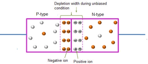
In this case, no external voltage is applied to the P-N junction diode; and therefore, the electrons diffuse to the P-side and simultaneously holes diffuse towards the N-side through the junction, and then combine with each other. Due to this an electric field is generated by these charge carriers. The electric field opposes further diffusion of charged carriers so that there is no movement in the middle region. This region is known as depletion width or space charge.
|
Figure 13: Unbiased or zero biased PN Junction Diode
FORWARD BIAS
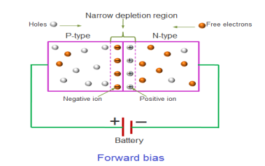
In the forward bias condition, the positive terminal of the battery is connected to the P-Type material and the negative terminal of the battery is connected to the N-type material. This connection is also called as giving positive voltage.
|
Figure 14: Forward bias
Electrons from the N-region cross the junction and enters the P-region. Due to the attractive force that is generated in the P-region the electrons are attracted and move towards the positive terminal. Simultaneously the holes are attracted to the negative terminal of the battery. By the movement of electrons and holes current flows. In this condition, the width of the depletion region decreases due to the reduction in the number of positive and negative ions.
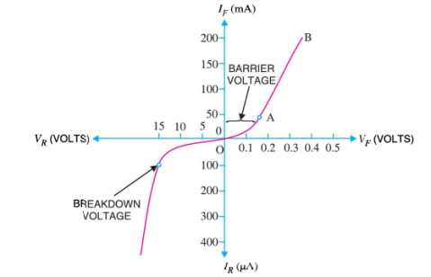
If this external voltage Vf becomes greater than the value of the potential barrier, approx. 0.7 volts for silicon and 0.3 volts for germanium, the potential barriers opposition will be overcome and current will start to flow.
This is because the negative voltage pushes or repels electrons towards the junction giving them the energy to cross over and combine with the holes being pushed in the opposite direction towards the junction by the positive voltage. This results in a characteristics curve of zero current flowing up to this voltage point, called the “knee” on the static curves and then a high current flow through the diode with little increase in the external voltage as shown in I-V characteristics.
REVERSE BIAS
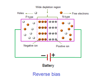
In the reverse bias condition, the negative terminal of the battery is connected to the P-type material and the positive terminal of the battery is connected to the N-type material. This connection is also known as giving negative voltage.
|
Figure 15: Reverse bias
The positive voltage applied to the N-type material attracts electrons towards the positive electrode and away from the junction, while the holes in the P-type end are also attracted away from the junction towards the negative electrode.
The net result is that the depletion layer grows wider due to a lack of electrons and holes and presents a high impedance path, almost an insulator. The result is that a high potential barrier is created thus preventing current from flowing through the semiconductor material.
This condition represents a high resistance value to the PN junction and practically zero current flows through the junction diode with an increase in bias voltage. However, a very small leakage current does flow through the junction which can be measured in micro-amperes, ( μA ).
If the reverse bias voltage Vr applied to the diode is increased to a sufficiently high enough value, it will cause the diode’s PN junction to overheat and fail due to the avalanche effect around the junction. This may cause the diode to become shorted and will result in the flow of maximum circuit current, and this shown as a step downward slope in the reverse static characteristics curve in I-V characteristics.
I-V CHARACTERISTICS OF PN JUNCTION DIODE
The I-V Characteristic Curves, which is short for Current-Voltage Characteristic Curves or simply I-V curves of an electrical device
The application of a forward biasing voltage on the junction diode results in the depletion layer becoming very thin and narrow which represents a low impedance path through the junction thereby allowing high currents to flow. The point at which this sudden increase in current takes place is represented on the static I-V characteristics curve above as the “knee” point. The current starts increasing with increase in voltage. At knee voltage current shows a sharp increment in its magnitude. This behaviour is mentioned above. As large current flow in forward biasing so we measure this current in mA.
When a junction diode is Reverse Biased, the thickness of the depletion region increases and the diode acts like an open circuit blocking current flow. So only a very small leakage current will flow.
|
Figure 16: I-V characteristics
Key Takeaways
- A P-N Junction Diode is formed by doping one side of a piece of silicon with a P-type dopant (Boron) and the other side with a N-type dopant (phosphorus). Ge can be used instead of Silicon.
- Zero biased condition is the case when no external voltage is applied to the P-N junction diode.
- In the forward bias condition, the positive terminal of the battery is connected to the P-Type material and the negative terminal of the battery is connected to the N-type material. This connection is also called as giving positive voltage.
- In the reverse bias condition, the negative terminal of the battery is connected to the P-type material and the positive terminal of the battery is connected to the N-type material. This connection is also known as giving negative voltage.
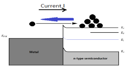
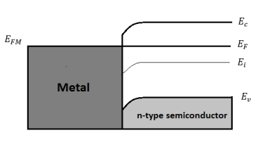
As the name implies, the MS junction is that a metal and a semiconductor material are contacted closely. The metal-semiconductor (MS) contact is an important component in the performance of most semiconductor devices in the solid state.
For the ideal MS contact, several assumptions are made:
The metal and the semiconductor are contacted intimately, which means that there is no oxide or charge layers between the contact on the atomic scale.
No intermixing and inter diffusion between the metal and the semiconductor.
There are no impurities at the MS interface.
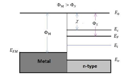
The principle of forming different types of the metal-semiconductor contact is the mismatch of the Fermi energy between metal and semiconductor material, which is due to the difference in work functions.
Φ work function = Φ is defined as the energy difference between the Fermi energy and the vacuum level.
χ electron affinity= χ is defined as the required energy for moving an electron from the vacuum level to the conduction band
E0 = the minimum energy needed to release an electron from the material, is used to align the metal and the semiconductor together.
The metal work function ΦM
The semiconductor work function ΦS
χ = (E0−Ec)FB|surface |
|
Figure 17: Energy band diagram for ideal MS contacts at an instant after contact for ΦM>ΦS and
|
Figure 18: Energy band diagram for ideal MS contacts at an instant after contact for ΦM<ΦS
χ and Φ are invariant fundamental properties that are remain unaffected by the contacting process. However, the work function of semiconductors is related with the electron affinity, the conduction band, and the Fermi energy:
ΦS=χ+ (Ec−EF)FB χ= (E0−EF) |
However, the situations in Figure 19 and 20 are not in equilibrium condition, since the Fermi energy in the metal is not aligned with the Fermi energy in semiconductor (EFS≠EFM).
Therefore, electrons will keep transferring between the semiconductor and the metal until the EF is aligned, which would cause a formation of depletion region between the MS contact. With different characteristics of the metal-semiconductor interface, two types of MS contact will be formed. We will discuss here.
There are two kinds of metal–semiconductor junction.
Rectifying Schottky Diodes
Non-rectifying Ohmic contact
Rectifying Schottky Diodes
The junctions between metal and lightly doped semiconductors exhibit rectifying IV- characteristics similar to those of PN junctions. They are called Schottky diodes and have some interesting applications.
Under a forward bias (VA>0)
|
Figure 19: Energy band diagram and carrier activity at forward biasing (VA>0)
Under Reverse Biasing VA<0
|
Figure 20: Energy band diagram and carrier activity at reverse biasing VA<0
I−V Characteristics
In general, the current flowing through the Schottky contact can be defined with the applied voltage, which is very similar to those of pn-junction diode. The IV expression is:
I=I0(eqVA/kT−1), |
where
I0 is a saturate current
Figure 21: I−V Characteristics
Non-rectifying Ohmic Contact
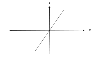
The junction between metal and heavily doped semiconductors behaves as low-resistance ohmic contacts (basically electrical shorts). Ohmic contacts are an important part of semiconductor devices and have a significant influence on the performance of high-speed transistors
|
Figure 22: Energy band diagram under equilibrium for ΦM<ΦS
|
Figure 23: IV characteristics of Ohmic contact
Whenever a metal and a semiconductor are in intimate contact, there exists a potential barrier between them to stop most charge carriers (i.e. electrons or holes) to flow from one to the other. Only a small number of carriers have enough energy to get over the barrier and cross to the other material.
Points keep in mind
- Lower the barrier height
The barrier height is a property of the materials we use. We try to use materials whose barrier height is small. Annealing can create an alloy between the semiconductor and the metal at the junction, which can also lower the barrier height. - Make the barrier very narrow
One very interesting property of very tiny particles like electrons and holes is that they can "tunnel" through barriers that they don't have enough energy to just pass over. The probability of tunnelling becomes high for extremely thin barriers (in the tens of nanometers). We make the barrier very narrow by doping it very heavily (1019 dopant atoms/cm3 or more).
When a bias is applied to the junction, it can have one of two effects: it can make the barrier appear lower from the semiconductor side, or it can make it appear higher. The bias does not change the barrier height from the metal side. The result of this is a Schottky Barrier (rectifying contact)
In Schottky Barrier (rectifying contact) the junction conducts for one bias polarity, but not the other. Almost all metal-semiconductor junctions will exhibit some of this rectifying behaviour. Schottky Contacts make good diodes, and can even be used to make a kind of transistor.
For getting signals into and out of a semiconductor device, we generally want a contact that is Ohmic. Ohmic contacts conduct the same for both polarities. (They obey Ohm's Law).There are two ways to make a metal-semiconductor contact look ohmic enough to get signals into and out of a semiconductor (or doing the opposite makes a good Schottky contact).
Key Takeaways
- The metal-semiconductor (MS) contact is an important component in the performance of most semiconductor devices in the solid state.
- The principle of forming different types of the metal-semiconductor contact is the mismatch of the Fermi energy between metal and semiconductor material, which is due to the difference in work functions.
- There are two kinds of metal–semiconductor junction: Rectifying Schottky Diodes and Non-rectifying Ohmic contact.
Unlike the majority of electronic devices, which are silicon based, optoelectronic devices are predominantly made using three to four semiconductor compounds such as GaAs, InP, GaN, and GaSb, and their alloys due to their direct-band gap.
Understanding the properties of these materials has been of vital importance in the development of optoelectronic devices. Since the first demonstration of a semiconductor laser in the early 1960s, optoelectronic devices have been produced in their millions, pervading our everyday lives in communications, computing, entertainment, lighting, and medicine. It is perhaps their use in optical-fiber communications that has had the greatest impact on humankind, enabling high-quality and inexpensive voice and data transmission across the globe.
Types of Optoelectronics Devices
Optoelectronics are classified into different types such as
- Photodiode
- Solar Cells
- Light Emitting Diodes
- Laser Diodes
- Optical Fibre
PHOTO DIODE
Silicon photo diode is a light sensitive device. It is also called as photo detector. Photo diode converts light signals into electrical signals. It is always operated in reverse biased condition.
Symbol
Figure 24: Symbol of Photo Diode
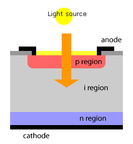
A photo diode is a semiconductor light sensor that generates a voltage or current when light falls on the junction. It consists of an active P-N junction, which is operated in reverse bias. When a photon with plenty of energy strikes the semiconductor, an electron or hole pair is created. The electrons diffuse to the junction to form an electric field.
|
Figure 25: Photodiode
The magnitude of photo current depends on the number of charge carriers generated and, on the light, falling of diode element. The current is also affected by the frequency of the light falling on the diode element. The magnitude of current under large reversed bias is given by
I =Is +I0(1 + exp(V/ηVT) |
Where Is = short circuit current which is proportional to the light intensity
I0 Reverse saturation current
V Voltage across the diode
VT Volt equilent of temperature
η Parameter, 1 for Ge, 2 for Si
Applications
- Photo diodes are used as
- Light detectors
- Demodulators
- Encoders
- Optical communication system
- High speed counting and switching circuits.
SOLAR CELLS
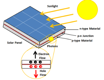
A solar cell or photo-voltaic cell is an electronic device that directly converts sun’s energy into electricity. When sunlight falls on a solar cell, it produces both a current and a voltage to produce electric power.
Sunlight, which is composed of photons, radiates from the sun. When photons hit the silicon atoms of the solar cell, they transfer their energy to lose electrons; and then, these high-energy electron flow to an external circuit.
|
Figure 26: Solar Cell
The solar cell is composed of two layers which are struck together. The first layer is loaded with electrons, so these electrons are ready to jump from the first layer to the second layer. The second layer has some electrons taken away, and therefore; it is ready to take more electrons.
The advantages of solar cells are that, there is no fuel supply and cost problem. These are very dependable and require little maintenance.
LIGHT EMITTING DIODE
Light emitting diode is a pn junction device. It is always operated in forward biased condition. LED converts electrical energy into light energy. In the fabrication of LED’s direct band gap semiconductors like GaP, GaAsP are used. In direct band gap semiconductors, most of the energy is emitted in the form of light when hole and electron recombination takes place.
|
Figure 27: LED
When an LED is forward biased the electrons and holes move in towards the junction and recombination takes place. As a result of recombination, the electrons lying in the conduction band of an n- region fall into the holes lying in the valence band of a p –region. The difference of energy in the valence band and conduction band is radiated in the form of light energy. Here their excess energy is transferred to the emitted photon. The brightness of emitted light is directly proportional to the forward bias current.
The usage of LED is advantageous as it consumes less power and produces less heat. LEDs last longer than incandescent lamps.
Applications LEDs are used in
- For instrument display
- In calculators
- Digital clocks
- For indicating power ON/ OFF
- For optical switching application
- In optical communication system
- Medical devices
LASER DIODE
Direct band gap semiconductors are preferred in the fabrication of laser diodes because they emit energy in terms of light when an electron and hole recombination takes place. These are operated at forward biased condition. Compound semiconductors like GaAS and InP are examples for direct band gap semiconductors.
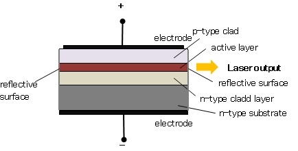
|
Figure 28: Laser Diode
The semiconductor laser device is always operated in forward bias condition. Electrons and the holes are the minority charge carriers in p-region and p-region semiconductors. When a huge current (104 Amp/mm2) is passing through the p-n junction, p-region is positively biased, holes are injected into n-region from p-region and n-region is negatively biased electrons are injected into p-region from n-region
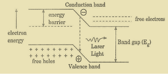
The continuous injection of charge carriers creates the population inversion of minority carriers in n and p sides’ respectively. The electrons and holes recombine and release of light energy takes place in or near the junction as shown in figure 29. The emitted photons increase the rate of recombination of injected electrons from the n-region and holes in p-region by inducing more recombinations.
For GaAs semiconductor Eg =1.4eV
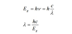
From Planck’s law Eg =hc/λ
From here λ = hc/ Eg =8874 Å
The wave length of emitted radiation depends up on the concentration of donor and acceptor atoms in GaAs. .In case of GaAs homo-junction which has an energy gap of 1.44eV gives a laser beam of wave length around 8874 Å. The efficiency of the laser emission is increases when we cool the GaAs diode.
OPTICAL FIBRE
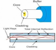
An optical fibre or optic fibre is a plastic and transparent fibre made of plastic or glass. It is somewhat thicker than a human hair. It can function as a light pipe or waveguide to transmit light between the two ends of the fibre.
Optical fibres usually include three concentric layers: a core, a cladding and a jacket. The core, a light transmitting region of the fibre, is the central section of the fibre, which is made of silica. Cladding, the protective layer around the core, is made of silica. This creates an optical waveguide that limits the light in the core by total reflection at the interface of the core-cladding. Jacket, the non-optical layer around the cladding, typically consists of one or more layers of a polymer that protect the silica from the physical or environmental damage.
|
Figure 29: Optical Fibre
Along with the fibre-optic cable, jackets are available in different colour. These colours allow the recognition of the fibre-optic cable and the type of cable one is dealing with. For example, an orange-colour cable clearly indicates a single-mode fibre, while a yellow one indicates a multimode fibre. In the single-mode fibre, one mode propagates and the light rays travel straight through the cable. In a multimode cable, the light rays travel through the cable following different modes.
Application
These cables are used in telecommunications, sensors, fibre lasers, bio-medicals and in many other industries. The advantages of using optical-fibre cable include their higher bandwidth, less signal degradation, weightlessness and thinness than a copper wire, cost-effectiveness, flexibility, and hence they are used in medical and mechanical imaging systems.
Key Takeaways
- Optoelectronic devices are predominantly made using three to four semiconductor compounds such as GaAs, InP, GaN, and GaSb, and their alloys due to their direct-band gap.
- Optoelectronics are classified into different types such as Photodiode, Solar Cells, Light Emitting Diodes, Laser Diodes and Optical Fibre
Optical Transitions in Bulk Semiconductors
- In semiconductors electrons can make transitions between two energy states and generate or destroy photons in the process.
- In particular, transitions between the conduction band (EC) and the valence band ( EV) are optically active.
- As the lower conduction band generally consists of s-like states while the upper valence band contains of p-like states.
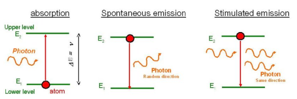
- Spontaneous emission, absorption, and stimulated emission can all take place between conduction band (EC) states and valence band (EV) states.
Absorption
- Similar to stimulated absorption in optics in the semiconductor absorption all we need is an incoming photon, a valence band energy state occupied by an electron, and an empty conduction band energy state.
- We know that in equilibrium condition, the valence band is fully occupied and the conduction band is empty.
- We know that for optical absorption between two states in an atom only occurred for a narrow spectrum of photon energies so here in optical absorption in a semiconductor can occur over a wide range of photon energies.
- This process carry out when the energy photon is greater than or equal to the band gap energy.
|
Figure 30: Spontaneous emission, absorption, and stimulated emission
- Incoming photon interacts with electron in valence band and provides it sufficient energy for excitation and by getting enough energy the electron jump to conduction band and leaving hole in valence band.
- The absorption process creates an electron in the conduction band and a hole in the valence band, it is also called optical generation.
- If the electrons created at energies higher than the band edge will quickly stabilize to the lowest conduction band energy states by releasing phonons.
- Holes created deep in the valence band will ‘float up’ to the valence band edge.
Spontaneous Emission
- Consider the system is in equilibrium but temperature is increased let us consider it is at T temperature.
- Electrons and holes can be created by optical absorption and other pumping mechanisms.
- The spontaneous emission process is possible for a wide range of photon energies above the band gap similar to absorption.
- At T temperature the lowest energy states are mostly full in conduction band.
- At T temperature the highest energy states are mostly empty in valence band.
- Therefore, the spontaneous emission observed in semiconductor in which photon has energy nearly equal to the band gap energy.
- Since the spontaneous emission process ‘destroys’ an electron and a hole, it is also called spontaneous optical recombination.
Why ordinary silicon is not useful for light emission?
Why stimulated emission process is not carrying out in indirect band gap semiconductors?
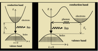
Silicon has an indirect band gap. That means that the lowest energy states in the conduction band have a different momentum than the highest energy states in the valence band.
As we discussed above At T temperature the lowest energy states are mostly full in conduction band and the highest energy states are mostly empty in valence band. So these are the states that are most likely to be occupied by an electron and a hole.
The spontaneous emission process must conserve both energy and momentum, but photons carry very little momentum but it is not zero have some finite value.
Therefore, an electron at the ‘bottom’ of the conduction band is unable to recombine with a hole at the ‘top’ of the valence band via spontaneous photon emission, because that would violate conservation of momentum: the electron would have to undergo a significant momentum change, and the photon is unable to carry away enough momentum.
This is the reason ordinary silicon is not useful for light emission and stimulated emission process is not carrying out in indirect band gap semiconductors.
Stimulated emission
- The stimulated emission process ‘destroys’ an electron and a hole, it is also called stimulated optical recombination.
- In order to make stimulated emission the dominant optical process, we need to achieve population inversion.
- It is the most important process for laser operation.
- In this process a copy of the incoming photon is produced.
- we expect that in most cases the stimulated emission will occur primarily between band-edge states, as these states are most likely to be occupied with electrons and holes just like in spontaneous emission.
- Semiconductor optical amplifiers generally amplify light whose photon energy is approximately equal to the band gap energy of the semiconductor gain medium.
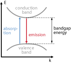
|
Figure 31: Spontaneous emission, absorption, and stimulated emission and E-K diagram
Key Takeaways
- In semiconductors electrons can make transitions between two energy states and generate or destroy photons in the process.
- In particular, transitions between the conduction band (EC) and the valence band ( EV) are optically active.
- As the lower conduction band generally consists of s-like states while the upper valence band contains of p-like states.
- Spontaneous emission, absorption, and stimulated emission can all take place between conduction band (EC) states and valence band (EV) states.
Introduction
LASER stands for “Light Amplification by Stimulated Emission of Radiation”.
L = Light
A = Amplification (by)
S = Stimulated
E = Emission (of)
R = Radiation
The principle of laser amplification is stimulated emission.
Let us discuss Einstein’s theory of the interaction of electromagnetic radiation with matter. He proposed that electromagnetic radiation interacts with matter in the following three steps.
- Stimulated Absorption
- Spontaneous Emission
- Stimulated Emission
Stimulated Absorption:
Let E1 and E2 be the energies of the ground and excited states of an atom. Suppose, if a photon of energy hν= E1− E2 interacts with an atom present in the ground state, the atom gets excitation from ground state E1 to excited state E2. This process is called stimulated absorption. Stimulated absorption rate depends upon the number of atoms available in the lowest energy state as well as the energy density photons.
Stimulated absorption rate ∝ Number of atoms in the ground state ∝ The density of photons Spontaneous emission |
|
Figure 32: Interaction of Radiation with Matter
Spontaneous Emission:
Let E1 and E2 be the energies of the ground and excited states of an atom. Suppose, if a photon of energy hν= E1− E2 interacts with an atom present in the ground state, the atom gets excitation from ground stateE1 to excited state E2. The excited atom does not stay a long time in the excited state. The excited atom gets de-excitation after its lifetime by emitting a photon of energy hν= E1− E2. This process is called spontaneous emission. Also Spontaneous means by its own. Here excited atom comes to the ground state on its own so it is named as spontaneous emission.
The spontaneous emission rate depends upon the number of atoms present in the excited state.
Spontaneous emission ∝ rate number of atoms in the excited state
Stimulated Emission:
This phenomenon is responsible for producing laser light. Let E1and E2 be the energies of the ground and excited states of an atom. Suppose, if a photon of energy hν= E1− E2 interacts with an atom present in the ground state, the atom gets excitation from ground stateE1 to excited state E2. Let, a photon of energy hν= E1− E2 interacts with the excited atom within their lifetime; the atom gets de-excitation to the ground state by emitting another photon. These photons have the same phase and it follows coherence. This phenomenon is called stimulated emission.
Stimulated emission rate depends upon the number of atoms available in the excited state as well as the energy density of photons.
Stimulated emission rate ∝ number of atoms in the excited state ∝ Density of photons |
EINSTEIN’S COEFFICIENTS
The distribution of atoms in the two energy levels will change by absorption or emission of radiation. Einstein introduced three empirical coefficients to quantify the change of population of the two levels. Let N1 be the number of atoms per unit volume with energy E1 and N2 be the number of atoms per unit volume with energy E2. Let ‘n’ be the number of photons per unit volume at frequency ‘υ’ such that hυ= E1− E2.
Then, the energy density of photons ρ(υ) = nhυ
|
Figure 33: Interaction of photons with atoms
When these photons interact with atoms, both upward (absorption) and downward (emission) transition occurs.
At the equilibrium, the upward transitions must be equal to downward transitions.
Upward Transition
Stimulated absorption rate depends upon the number of atoms available in the lowest energy state as well as the energy density photons.
We have seen above that
Stimulated absorption rate ∝ N1 i.e. Number of atoms in the ground state ∝ ρ(υ) i.e. Density of photons spontaneous emission Stimulated absorption rate = B12N1ρ(υ) ………(1)
|
Where B12 is the Einstein coefficient of stimulated absorption.
Downward transition
The spontaneous emission rate depends upon the number of atoms present in the excited state.
Spontaneous emission rate ∝ N2 i.e. number of atoms in the excited state
Spontaneous emission rate = A21N2 ………(2) |
Where A21 is the Einstein coefficient of spontaneous emission.
Stimulated emission rate depends upon the number of atoms available in the excited state as well as the energy density of photons.
Stimulated emission rate ∝ N2 i.e. number of atoms in the excited state ∝ ρ(υ) i.e. Density of photons Stimulated emission rate = B21N2ρ(υ) ………(3) |
If the system is in equilibrium the upward transitions must be equal to downward transitions.
upward transitions = downward transitions
B12N1ρ(υ) = A21N2 + B21N2ρ(υ) ………(4) B12N1ρ(υ) - B21N2ρ(υ) = A21N2 (B12N1- B21N2) ρ(υ) = A21N2 ρ(υ) = |
Divide with B21N2 in numerator and denominator in the right side of the above equation,
ρ(υ) = ρ(υ) = |
We know from Maxwell Boltzmann distribution law
|
And also from Planck’s law, the radiation density
ρ(υ) = |
Comparing the two equations (7) and (9)
|
The above relations are referred to as Einstein relations.
From the above equation for non-degenerate energy levels, the stimulated emission rate is equal to the stimulated absorption rate at the equilibrium condition.
|
Key Takeaways
- LASER stands for “Light Amplification by Stimulated Emission of Radiation”.
- Einstein gave his theory of the interaction of electromagnetic radiation with matter. He proposed that electromagnetic radiation interacts with matter in the following three steps. Stimulated Absorption, Spontaneous Emission and Stimulated Emission
- Stimulated absorption rate depends upon the number of atoms available in the lowest energy state as well as the energy density photons.
- The spontaneous emission rate depends upon the number of atoms present in the excited state.
- Stimulated emission rate depends upon the number of atoms available in the excited state as well as the energy density of photons.
- The Einstein relations is given as
 =
= and
and  =1
=1
Definition
The number of atoms present in the excited state or higher energy state is greater than the number of atoms present in the ground state or lower energy state is called population inversion.
Population inversion as the name suggests that this is an inverted phenomenon. In general, the lower energy level is more populated which means it has more number atoms in the lower energy level as compared to a higher energy level. But by pumping we will obtain a state when the number of atoms present in the higher energy state is greater than the number of atoms present in the lower energy state.
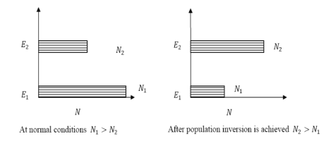
Let us consider a two-level energy system of energies E1 and E2 as shown in the figure.
Let N1 and N2 be the populations that mean several atoms per unit volume of energy levels E1 and E2 respectively.
According to Boltzmann’s distribution the population of an energy level E, at temperature T is given by
Ni=N0 |
Where N0 is the population of the lower level or ground state and k is Boltzmann’s constant.
From the above relation, the population of energy levels E1 and E2 are
N1=N0 N2=N0 |
At ordinary conditions N1 >N2 i.e., the population in the ground or lower state is always greater than the population in the excited or higher states. The stage of making, the population of higher energy level is greater than the population of lower energy level is called population inversion i.e. N1 < N2
|
Figure 34: Population inversion
When the population inversion method is used to enforce more and more atoms to give up photons. This initiates a chain reaction and releasing a massive amount of energy.
This results in a rapid build-up of the energy of emitting one particular wavelength traveling coherently in a fixed direction. This process is called amplification by stimulated emission using population inversion.
This population inversion situation is essential for laser action. For any stimulated emission, the upper energy level or metastable state must have a long lifetime, i.e., the atoms should pause at the metastable state for more time than at the lower level.
Key Takeaways
- The number of atoms present in the excited state or higher energy state is greater than the number of atoms present in the ground state or lower energy state is called population inversion.
- The condition of population inversion is given as N1 < N2
- The population inversion results in a rapid build-up of the energy of emitting one particular wavelength traveling coherently in a fixed direction. This process is called amplification by stimulated emission using population inversion.
Pumping mechanisms of population inversion
A system in which population inversion is achieved is called an active system. The method of raising the particles from a lower energy state to a higher energy state is called pumping.
The process of achieving population inversion is called pumping.
This can be done in several ways.
The most commonly used pumping methods are
- Optical pumping
- Electrical discharge pumping
- Chemical pumping
- Thermal Pumping
- Injection current pumping
- Inelastic Atom-Atom Collisions
Examples of optically pumped lasers are ruby, Nd: YAG Laser (Neodymium: Yttrium Aluminium Garnet).
Electrical discharge pumping is used in gas lasers. Since gas lasers have a very narrow absorption band pumping then any flash lamp is not possible. Electric discharge refers to the flow of electrons or electric current through a gas, liquid, or solid.
In this method of pumping, electric discharge acts as the pump source or energy source. A high voltage electric discharge (flow of electrons, electric charge, or electric current) is passed through the laser medium or gas. The intense electric field accelerates the electrons to high speeds and they collide with neutral atoms in the gas. As a result, the electrons in the lower energy state gains sufficient energy from external electrons and jumps into the higher energy state
Examples of Electrical discharge pumped lasers are He-Ne laser, CO2 laser, argon-ion laser, etc.
Chemical pumping Chemical reaction may also result in excitation and hence the creation of population inversion in a few systems.
If an atom or a molecule is produced through some chemical reaction and remains excited at the time of production, then it can be used for pumping. The hydrogen fluoride molecule is produced in an excited state when hydrogen and fluorine gas chemically combine. The number of produced excited atoms or molecules is greater than the number of normal state atoms or molecules. Thus, population inversion is achieved.
Examples H2 + F2 → 2HF, in this chemical reaction, hydrogen (H2) and fluorine (F2) molecules are chemically combined to produce hydrogen fluoride molecule (2HF) in an excited state.
Thermal Pumping: Sometimes we can achieve population inversion by heating the laser medium. In thermal pumping, heat acts as the pump source or energy source. In this method, population inversion is achieved by supplying heat into the laser medium.
When heat energy is supplied to the laser medium, the lower energy state electrons gain sufficient energy and jumps into the higher energy level.
The process of achieving population inversion in thermal pumping is almost similar to the optical pumping or electric discharge method, except that in this method heat is used as a pump source instead of light or electric discharge.
Injection current pumping In semiconductors, injection of current through the junction results in creates of population inversion among the minority charge carriers.
Examples of such systems are InP and GaAs.
When high voltage electric discharge passes through a laser medium having two types of gases X and Y, the lower energy state electrons in gas X will move to the exciting state X+ similarly the lower energy state electrons in gas Y moves to the excited state Y+.
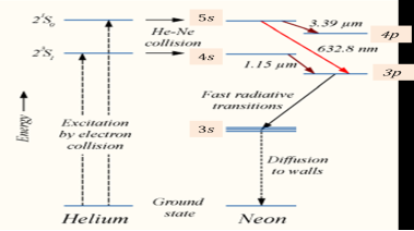
Initially, during electric discharge, the lower energy state electrons in gas X or atom X gets excited to X+ due to continuous collision with electrons. The excited state electrons in gas X+ now collide with the lower energy state electrons in gas Y. As a result, the lower energy state electrons in gas Y gains sufficient energy and jump into the exciting state Y+. This method is used in the Helium-Neon (He-Ne) laser.
THREE-LEVEL LASER
The two energy levels between which lasing occur are the lower laser energy level (E1), and the upper laser energy level (E2).
To simplify the explanation, we neglect spontaneous emission.
To achieve lasing, energy must be pumped into the system to create a population inversion. So, that more atoms will be in energy level E2 than in the ground level (E1).
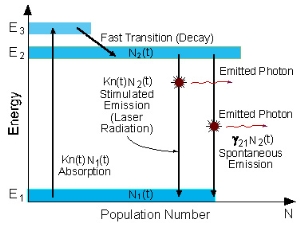
Atoms are pumped from the ground state (E1) to energy level E3. They stay there for an average time of 10-8 [sec], and decay (usually with a non-radiative transition) to the metastable energy level E2.
A schematic energy level diagram of a laser with three energy levels is shown in the figure,
|
Figure 35: Energy level diagram in a three-level laser
Since the lifetime of the metastable energy level (E2) is relatively long (of the order of 10-3 [sec], many atoms remain at this level. If the pumping is strong enough, then after pumping more than 50% of the atoms will be in energy level E2, a population inversion exists, and lasing can occur.
In a three-level system, the laser transition ends on the ground state. The unpumped gain medium exhibits strong absorption on the laser transition. A population inversion and consequently net laser gain result only when more than half of the ions (or atoms) are pumped into the upper laser level; the threshold pump power is thus fairly high.
The population inversion can be achieved only by pumping into a higher-lying level, followed by a rapid radiative or non-radiative transfer into the upper laser level, because in this way one avoids stimulated emission caused by the pump wave. (For transitions between only two levels, simultaneous pump absorption and signal amplification cannot occur.)
An example of a three-level laser medium is ruby (Cr3+:Al203), as used by Maiman for the first laser.
FOUR -LEVEL LASER
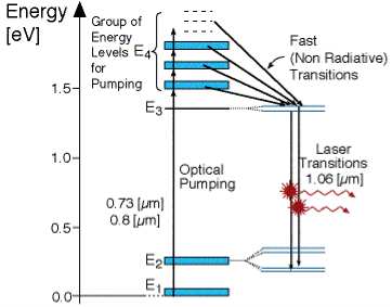
As seen in Figur, there are four energy levels, with energies E1, E2, E3, E4 with populations of N1, N2, N3, N4 respectively. There energies increase for each level so that E1 < E2 < E3 < E4.
|
Figure 36: Four level laser
In this system, optical pumping from the ground state (E1 ) into the pump band (E4) excites the atoms. From this level, the atoms decay by a fast, radiationless transition into level 3 (E3). The lifetime of the laser transition from E3 – E2 is long compared to that of E4 –E3, a population accumulates in this level 3 (lasing level).
Here the atoms relax and start to create laser transitions through spontaneous and stimulated emissions into level 2 (E2). At this level, level 4 has a fast decay into the ground state. Like before this quickly de-excited atom leads to a negligible population in E2.
This is significant, as the highly populated E3 level will then form a population inversion with the E2 level. Specifically, as long as the population of level 3 N3 is greater than 0. Therefore optical amplification and laser operation can take place.
Since only a small number of atoms need to be excited in the upper lasing level E3 to form population inversion, it proves that a 4 level laser is much more efficient and practical than a 3 level laser.
A lower threshold pump power can be achieved with a four-level laser medium, where the lower laser level is well above the ground state and is quickly depopulated e.g. by multi-photon transitions. Ideally, no appreciable population density in the lower laser level can occur even during laser operation. In that way, reabsorption of the laser radiation is avoided (provided that there is no absorption on other transitions). This means that there is no absorption of the gain medium in the unpumped state, and the gain usually rises linearly with the absorbed pump power.
The most popular four-level solid-state gain medium is Nd: YAG. All lasers based on neodymium-doped gain media, except those operated on the ground-state transition around 0.9-0.95 pm, are four-level lasers.
Neodymium ions can also be directly pumped into the upper laser level, e.g. with pump light around 880 nm for Nd: YAG. Even though effectively only three levels are involved, the term three-level system would not be used here.
Key Takeaways
- For laser action, the pumping mechanism (exciting with external source) maintain a higher population of atoms in the upper energy level relative to that in the lower level.
- A system in which population inversion is achieved is called an active system. T
- The process of achieving population inversion is called pumping.
- Pumping can be done in several ways. The most commonly used pumping methods are Optical pumping, Electrical discharge pumping, Chemical pumping Thermal Pumping, Injection current pumping , Inelastic Atom-Atom Collisions
3.12.1 CONSTRUCTION AND WORKING OF RUBY LASER
Construction
A ruby laser consists of three important elements: laser medium, the pump source, and the optical resonator.
Laser Medium
Ruby (Al2O3+Cr2O3) is a crystal of Aluminium oxide, in which 0.05% of Al+3 ions are replaced by the Cr+3 ions. The colour of the rod is pink. The active medium or laser medium in the ruby rod is Cr+3 ions. In ruby laser, 4cm length and 5mm diameter rod is generally used. The ruby has good thermal properties.
|
Figure 37: Ruby laser
The pump source
We know that population inversion is required to achieve laser emission. Population inversion is the process of achieving a greater population of a higher energy state than the lower energy state. To achieve population inversion, we need to supply energy to the laser medium i.e. to ruby crystal.
Xenon flash tube emits thousands of joules of energy in few milliseconds, but only a part of that energy is utilized by the chromium ions while the rest energy heats the apparatus. A cooling arrangement is provided to keep the experimental set up at normal temperatures.
Optical resonator
Working of ruby laser:
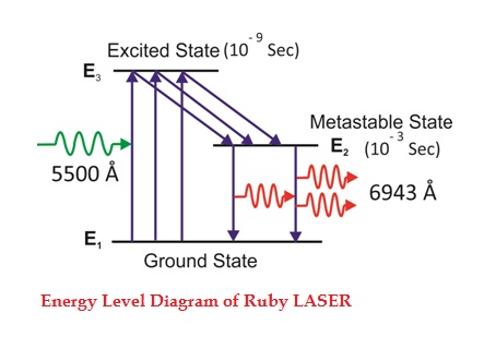
Consider a ruby laser medium consisting of three energy levels E1, E2, E3 with N number of electrons.
We assume that the energy levels will be E1 < E2 < E3. The energy level E1 is known as the ground state or lower energy state, the energy level E2 is known as the metastable state, and the energy level E3 is known as the pump state.
Let us assume that initially most of the electrons are in the lower energy state (E1) and only a tiny number of electrons are in the excited states (E2 and E3).
The energy level diagram of chromium ions is shown in the figure. The chromium ions get excitation into higher energy levels by absorbing 5500Å of wavelength radiation. The excited chromium ions stay in the level E3 for a short interval of time (10-8 to 10-9 Sec). After their life, most of the chromium ions are de-excited from E3 to E1 and a few chromium ions are de-excited from E3 to E2.
Figure 38: Energy Level diagram of ruby laser
The transition between E3 and E2 is non-radioactive i.e. the chromium ions give their energy to the lattice in the form of heat. In the Metastable state, the lifetime of chromium ions is 10-3 sec. The lifetime of chromium ions in the Metastable state is 105 times greater than the lifetime of chromium ions in a higher state.
Due to the continuous working of the flash lamp, the chromium ions are excited to a higher state E3 and returned to the E2 level. After a few milliseconds, the level E2 is more populated than the level E1 and hence the desired population inversion is achieved. The state of population inversion is not a stable one. The process of spontaneous transition is very high. When the excited chromium ion passes spontaneously from E3 to E2it emits one photon of wavelength 6943 Å. The photon reflects back and forth by the silver ends and until it stimulates an excited chromium ion in the E2 state and it to emit a fresh photon in phase with the earlier photon. The process is repeated again and again until the laser beam intensity is reached a sufficient value. When the photon beam becomes sufficiently intense, it emerges through the partially silvered end of the rod. The wavelength 6943 Å is in the red region of the visible spectrum.
Drawbacks of the ruby laser
- The laser requires high pumping power
- The efficiency of a ruby laser is very small
- It is a pulse laser
Application of ruby laser
- Ruby lasers are in optical photography
- Ruby lasers can be used for the measurement of plasma properties such as electron density and temperature.
- Ruby lasers are used to remove the melanin from the skin.
- Ruby laser can be used for the recording of holograms.
Key Takeaways
- Ruby laser is a three-level solid-state laser.
- A ruby laser consists of three important elements: laser medium, the pump source, and the optical resonator.
- Ruby laser is one of the few solid-state lasers that produce visible light. It emits deep red light of wavelength 694.3 nm.
3.12.2 HELIUM - NEON GAS LASER
Ruby laser is a pulse laser, even it has high intense output. For continuous laser beams, gas lasers are used. Using gas lasers, we can achieve high coherence, high directionality, and high monochromaticity beam. The output power of the gas laser is generally in few milliwatts.
CONSTRUCTION
The helium-neon laser consists of three essential components:
- Pump source (high voltage power supply)
- Gain medium (laser glass tube or discharge glass tube)
- Resonating cavity
Pump source
The gain medium of a helium-neon laser is made up of a mixture of helium and neon gas contained in a glass tube at low pressure. In the He-Ne gas laser, the He and Ne gases are taken in the ratio 10:1 in the discharge tube.
Gain medium
In He-Ne laser 80cm length and 1cm diameter discharge are generally used. The out power of these lasers depends on the length of the discharge tube and the pressure of the gas mixture. Therefore, to achieve population inversion, we need to pump electrons from the lower energy state of the helium. In He-Ne laser, neon atoms are the active centres and have energy levels suitable for laser transitions while helium atoms help in exciting neon atoms.
Figure 39: He-Ne Laser
Two reflecting mirrors are fixed on either end of the discharge tube, in that, one is partially reflecting and the other is fully reflecting. The fully silvered mirror will completely reflect the light whereas the partially silvered mirror will reflect most of the light but allows some part of the light to produce the laser beam.
WORKING
When the electric discharge is passing through the gas mixture, the electrons accelerated towards the positive electrode. During their passage, they collide with He atoms and excite them into higher levels. 23s1 and 21s0 form the ground state of the He atom. In higher levels, 23s1 and 21s0, the lifetime of He atoms are more. So there is a maximum possibility of energy transfer between He and Ne atoms through atomic collisions. When He atoms present in the levels 23s1 and 21s0 collide with the Ne atom's present ground state, the Ne atoms get excitation into higher levels 4s and 5s.
Due to the continuous excitation of Ne atoms, we can achieve the population inversion between the higher levels 4s and 5s and lower levels 3p and 4p. The various transitions 5s to 4p, 4s to 3p, and 5s to 3p leads to the emission of wavelengths 3.93μm, 1.51μm, and 6328 Å or 632.8μm.
Figure 40: Energy Level diagram of He-Ne Laser
ADVANTAGES OF HELIUM-NEON LASER
- The helium-neon laser emits laser light in the visible portion of the spectrum.
- High stability
- Low cost
- Operates without damage at higher temperatures
DISADVANTAGES OF HELIUM-NEON LASER
- Low efficiency
- Low gain
- Helium-neon lasers are limited to low power tasks
APPLICATIONS OF HELIUM-NEON LASERS
- Helium-neon lasers are used in industries.
- Helium-neon lasers are used in scientific instruments.
Helium-neon lasers are used in the college laboratories
Key Takeaways
- Helium-Neon laser is a type of gas laser in which a mixture of helium and neon gas is used as a gain medium.
- The helium-neon laser was the first continuous-wave laser ever constructed.
- The helium-neon laser consists of three essential components Pump source (high voltage power supply),Gain medium (laser glass tube or discharge glass tube), Resonating cavity
- The helium-neon laser operates at a wavelength of 632.8 nanometres (nm), in the red portion of the visible spectrum.
3.12.3 SEMICONDUCTOR LASER
Semiconductor Laser
Semiconductor lasers represent one of the most important classes of lasers in use today, not only because of the large variety of direct applications in which they are involved but also because they have found widespread use as pumps for solid-state lasers.
Semiconductor lasers require, for the active medium, a direct gap material, and accordingly, the normal elemental semiconductors like Si or Ge cannot be used. The majority of semiconductor-laser materials are based on a combination of elements belonging to the third group of the periodic table such as Al, Ga, In with elements of the fifth group such as N, P, As, Sb. Examples include the best known GaAs as well as some ternary AlGaAs, InGaAs, and quaternary InGaAsP alloys.
InGaN semiconductor lasers the best candidates for semiconductor laser emission in the very important blue-green spectral region. Semiconductor laser materials are not limited to III–V compounds, however. For the blue-green end of the spectrum, we note that wide-gap semiconductors are using a combination between elements of the second group (such as Cd and Zn) and the sixth group (S, Se).
PRINCIPLE
When a p-n junction diode is forward biased, the electrons from the n – region and the holes from the p- region cross the junction and recombine with each other.
During the recombination process, the light radiation (photons) is released from a certain specified direct bandgap semiconductor like Ga-As. This light radiation is known as recombination radiation.
The photon emitted during recombination stimulates other electrons and holes to recombine. As a result, stimulated emission takes place which produces laser.
|
Figure 41: Semiconductor Laser
The basic structure of a semiconductor laser is shown in Figure. The active medium is a p-n junction diode made from the single crystal of gallium arsenide. The active layer called a light emission layer sandwiched between the p- and n-type clad layers i.e. double heterostructure is formed on an n-type substrate and voltage is applied across the p-n junction from the electrodes. This crystal is cut in the form of a platter having a thickness of 0.5μmm. Both edges of the active layer have a mirror-like surface. When a forward voltage is applied, electrons combine with holes at the p-n junction and emit the light.
This light is not a laser yet; it is confined within the active layer because the refractive index of the clad layers is lower than that of the active layer. Besides both ends of the active layer act as a reflecting mirror where the light reciprocates in the active layer. Then, the light is amplified by the stimulated emission process and laser oscillation is generated.
The photon emission is stimulated in a very thin layer of PN junction (in order of few microns). The electrical voltage is applied to the crystal through the electrode fixed on the upper surface. The end faces of the junction diode are well polished and parallel to each other. They act as an optical resonator through which the emitted light comes out.
|
Figure 42: Construction of semiconductor Laser
WORKING
The region around the junction contains a large number of electrons in the conduction band and a large number of holes in the valence band.
If the population density is high, a condition of population inversion is achieved. The electrons and holes recombine with each other and this recombination produces radiation in the form of light.
When the forward-biased voltage is increased, more and more light photons are emitted and the light production instantly becomes stronger. These photons will trigger a chain of stimulated recombination resulting in the release of photons in phase.
|
Figure 43: Energy Level diagram of Semiconductor Laser
After gaining enough strength, it gives out the laser beam of wavelength 8400Å. The nature of output is a continuous wave or pulsed output. The power output from this laser is 1mW. The wavelength of laser light is given by
|
Where Eg is the bandgap energy in joule.
ADVANTAGES
- It is very small in dimension.
- The arrangement is simple and compact.
- It exhibits high efficiency.
- It is operated with lesser power than a ruby and CO2 laser.
- The laser output can be easily increased by controlling the junction current
- It requires very little auxiliary equipment
- It can have a continuous wave output or pulsed output.
DISADVANTAGES
- It is difficult to control the mode pattern and mode structure of the laser.
- The output is usually from 5 degrees to 15 degrees i.e., the laser beam has a large divergence.
- The purity and monochromaticity are power than other types of laser
- Threshold current density is very large (400A/mm2).
- It has poor coherence and poor stability.
APPLICATION
- It is widely used in fibre optic communication
- It is used to heal the wounds by infrared radiation
- It is also used as a pain killer
- It is used in laser printers and CD writing and reading.
Key Takeaways
- It is a solid-state semiconductor laser. It is a specifically fabricated p-n junction diode.
- Semiconductor laser is based on the principle that when a p-n junction diode is forward biased, the electrons from the n – region and the holes from the p- region cross the junction and recombine with each other.
- During the recombination process, the light radiation (photons) is released from a certain specified direct bandgap semiconductor like Ga-As. This light radiation is known as recombination radiation.
- The photon emitted during recombination stimulates other electrons and holes to recombine. As a result, stimulated emission takes place which produces laser.
- A semiconductor laser is a device that causes laser oscillation by flowing an electric current to the semiconductor.
- Semiconductor lasers require, for the active medium, a direct gap material, and accordingly, the normal elemental semiconductors like Si or Ge cannot be used.
Reference
- J. Singh, ‘Semiconductor Optoelectronics: Physics and Technology’, McGraw Hill Inc.,1995.
- S.M. Sze, ‘Semiconductor Devices: Physics and Technology’, Wiley, 2008.
- Yariv and P. Yeh, ‘Photonics: Optical Electronics in Modern Communications’, Oxford University Press, New York, 2007.
- P. Bhattacharya, ‘Semiconductor Optoelectronic Devices’, Prentice Hall of India, 1997.
