UNIT – 2
BAND THEORY OF SOLIDS & SEMICONDUCTORS AND DIELECTRIC MATERIALS
REVIEW OF CLASSICAL FREE ELECTRON THEORY, MENTION OF FAILURES
The classical free electron theory of metals (Drude –Lorentz theory of metals) Drude and Lorentz proposed this theory in 1900. According to this theory, the metals containing the free electrons obey the laws of classical mechanics.
Assumptions (or salient features) in classical free electron theory
The classical free electron theory is based on the following postulates.
1. The valence electrons of atoms are free to move about the whole volume of the metal, like the molecules of a perfect gas in a container.
2. The free electrons move in random direction and collide with either positive ions fixed to the lattice or the other free electrons. All the collisions are elastic in nature i.e., there is no loss of energy.
3. The momentum of free electrons obeys the laws of the classical kinetic theory of gases.
4. The electron velocities in a metal obey classical Maxwell-Boltzman distribution of velocities.
5. When the electric field is applied to the metal, the free electrons are accelerated in the direction opposite to the direction of applied electric field.
6. The mutual repulsion among the electrons is ignored, so that they move in all the directions with all possible velocities.
7. In the absence of the field, the energy associated with an electron at temperature T is given by  kT. It is related to the kinetic energy equation
 kT =
kT =  v2th
v2th
Here vth represents the thermal velocity.
Success of classical free electron theory
1. It verifies ohm’s law
2. It explains electrical conductivity of metals.
3. It explains thermal conductivity of metals.
4. It derives Widemann – Franz law. (i.e. the relation between electrical and thermal conductivity.
Draw backs of classical free electron theory.
1. It could not explain the photoelectric effect, Compton Effect and black body radiation.
2. Electrical conductivity of semiconductors and insulators could not be explained.
3. Widemann – Franz law (K/σT= constant) is not applicable at lower temperatures.
4. Ferromagnetism could not be explained by this theory. The theoretical value of paramagnetic susceptibility is greater than the experimental value.
5. According to classical free electron theory the specific heat of metals is given by 4.5R whereas the experimental value is given by 3R.
6. According to classical free electron the electronic specific heat is equal to 3/2R while the actual value is 0.01R.
Electrical Conductivity
The classical free electron theory was proposed by Drude and Lorentz. According to this theory the electrons are moving freely and randomly moving in the entire volume of the metal like gas atoms in the gas container. When an electric field is applied the free electrons gets accelerated.
When an electric field E is applied between the two ends of a metal of area of cross section A
When an electrical field (E) is applied to an electron of charge ‘e’ of a metallic rod, the electron moves in opposite direction to the applied field with a velocity vd. This velocity is known as drift velocity.
Drift velocity vd is defined as the average velocity of the free electrons with which they move towards the positive terminal under the influence of the electrical field.
Lorentz force acting on the electron F = eE ........(1) This force is known as the driving force of the electron. Due to this force, the electron gains acceleration ‘a’. From Newton’s second law of motion, Force F = ma …....(2) From the equation (1) and (2), ma = eE or a = Acceleration (a) = Or a = Relaxation time is defined as the time taken by a free electron to reach its equilibrium position from the disturbed position in the presence of an electric field. So vd = a ……….(4) Substituting equation (3) in (4) vd = vd = Where The Ohms’ law states that current density (J) is expressed as J =E ……….(6) Or = Where is the electrical conductivity of the electron. But, the current density in terms of drift velocity is given as J = nevd ....... (7) Substituting equation (5) in equation (7), we have J = ne Or On comparing the equation (6) and (8) , we have Electrical conductivity = = This is a required expression for electrical conductivity. Resistivity ρ ρ = According to kinetic theory of gasses
So = Also ρ = Mobility: It is defined as the drift velocity of the charge carrier per unit applied electric field. μ= From equation (7) we have J = nevd by substituting vd =μE from equation (9) J = neμE Or We know by ohms law = = μne μ = This is the required expression for mobility.
|
Temperature Dependence
The positive ions are always in oscillating (or vibrating) state about their mean position; even the substance is present at 0k temperature. The vibrating amplitude of ions is always depends the temperature. The mean free path λ of the electrons is inversely proportional to the mean square of amplitude of ionic vibrations A0
λ =  ………(1)
The energy of lattice vibrations is proportional to  and increases linearly with temperature T.
 T ……….(2)
From equations (1) and (2)
λ =  ………..(3)
The resistivity ρ of the metal is inversely proportional to mean free path of electrons λ
ρ =  ..…………..(4)
From equations (3) and (4)
ρ T ..……….(5)
From equation (5) we observe that the resistivity of metal is linearly increases with temperature. The conductivity is defined as the reciprocal of resistance.

 ………….(6)
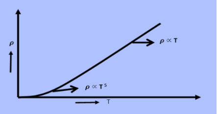
From equation (6) we observe that the conductivity of metal is inversely proportional to their temperature. The variation of resistivity of metal with temperature is shown in figure.
|
Figure 1: Variation of resistivity of metal with temperature
Key Takeaways
- According to this theory, the metals containing the free electrons obey the laws of classical mechanics.
- The valence electrons of atoms are free to move about the whole volume of the metal, like the molecules of a perfect gas in a container.
- The free electrons move in random direction and collide with either positive ions fixed to the lattice or the other free electrons. All the collisions are elastic in nature i.e., there is no loss of energy.
- Theory successfully explains the ohm’s law, electrical conductivity of metals and thermal conductivity of metals also give the relation between electrical and thermal conductivity.
- The required expression for electrical conductivity is given by =

- Resistivity ρ is given as ρ =
 =
= 
- Mobility is defined as the drift velocity of the charge carrier per unit applied electric field and given by μ =
 .
.
According to quantum free electron theory of metals, a conduction electron in a metal experiences constant (or zero) potential and free to move inside the crystal but will not come out of the metal because an infinite potential exists at the surface. This theory successfully explains electrical conductivity, specific heat, thermionic emission and paramagnetism. This theory is fails to explain many other physical properties, for example: (i) it fails to explain the difference between conductors, insulators and semiconductors, (ii) positive Hall coefficient of metals and (iii) lower conductivity of divalent metals than monovalent metals.
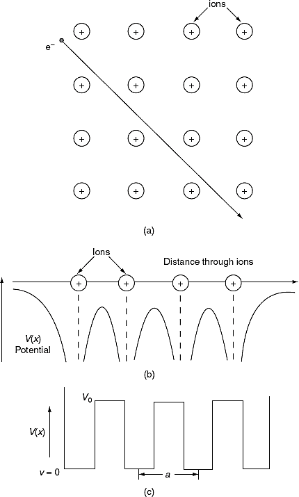
To overcome the above problems, the periodic potentials due to the positive ions in a metal have been considered as shown in Figure 2 (a), if an electron moves through these ions, it experiences varying potentials. The potential of an electron at the positive ion site is zero and is maximum in between two ions. The potential experienced by an electron, when it passes along a line through the positive ions is as shown in Figure 2 (b).
|
Figure 2: Periodic potentials due to the positive ions in a metal .
It is not easy to solve Schrödinger’s equation with these potentials. So, Kronig and Penney approximated these potentials inside the crystal to the shape of rectangular steps as shown in Figure 2(c). This model is called Kronig-Penney model of potentials.
|
Figure 3: called Kronig-Penney model of potentials.
The energies of electrons can be known by solving Schrödinger’s wave equation in such a lattice.
The solution to Schrödinger's equation for the Kronig-Penney potential is obtained by assuming that the solution is a Bloch function, namely a traveling wave solution of the form, eikx, multiplied with a periodic solution, u(x), which has the same periodicity as the periodic potential . The total wave function is therefore of the form:

where u(x) is the periodic function as defined by u(x) = u(x + a), and k(x) is the wave number. We now rewrite Schrödinger equation using this wave function considering first region I, between the barriers where V(x) = 0 and then region II, the barrier region where V(x) = V0:
In region I, Schrödinger's equation becomes:
with
Since the potential, V(x), is finite everywhere, the solutions for uI(x) and uII(x) must be continuous as well as their first derivatives. Continuity at x = 0 results in:
and continuity at x = a-b combined with the requirement that u(x) be periodic:
Finally, continuity of the first derivative at x = a-b, again combined with the requirement that u(x) is periodic, results in:
As a result we have four homogenous equations, (7), (9), (13), and (16), with four unknowns, A, B, C, and D, for which there will be a solution if the determinant of this set of equations is zero, or:
The first row of the determinant represents equation (7), the second row is obtained by combining (13) and (7), the third row represents equation (9) and the fourth row represents equation (16). This determinant can be rewritten as two determinants, each with three rows and columns, while replacing cosb(a-b) by bc, sinb(a-b) by bs, coshab eika by ac and sinhab eika by as, which results in:
|
where eika + e-ika was replaced by 2coska. Since the result is independent of the sign of k, this equation also covers all solutions obtained when replacing e-ik by eik in equations (5) and (6).
A further simplification is obtained as the barrier width, b, is reduced to zero while the barrier height, V0, is increased to infinity in such manner that the product, bV0, remains constant and the potential becomes a delta function train at x = a and repeated with a period of a, namely bV0 (x - b - na) where n is an integer. As b approaches zero, sinh b approaches b. Equation (20) then reduces to:
| (21) |
with |
| (22) |
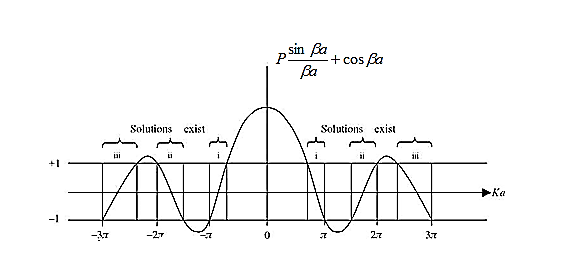
The right hand side of equation (21) shows the relation between the energy (through  ) and the wave-vector, k, and as you can see, since the left hand side of the equation can only range from −1 to 1 then there are some limits on the values that
  (and thus, the energy) can take, that is, at some ranges of values of the energy, there is no solution according to these equation, and thus, the system will not have those energies: energy gaps. These are the so-called band-gaps, which can be shown to exist in any shape of periodic potential (not just delta or square barriers). This has been plotted in Figure.
|
Figure 4: Graph of the right hand side of equation (21) of P for P =2
- The permissible limit of the term

lies between +1 to -1. By varying  a, a wave mechanical nature could be plotted as shown in Figure, the shaded portion of the wave shows the bands of allowed energy with the forbidden region as unshaded portion.
|
Figure 5 : Wave mechanical nature
2. With increase of  a , the allowed energy states for a electron increases there by increasing the band width of the bands, i.e., the strength of the potential barrier diminishes. This also leads to increase of the distance between electrons and the total energy possessed by the individual electron.
3.Conversly if suppose the effect of potential barrier dominate i.e., if P is large, the resultant wave obtained in terms of shows a stepper variation in the region lies between +1 to -1. This results in the decrease of allowed energy and increase of forbidden energy gap. Thus at extremities.
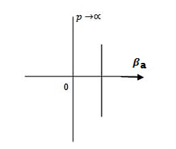
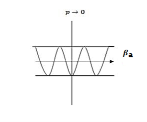
Case (i) when P , the allowed energy states are compressed to a line spectrum.
|
Figure 6: Allowed energy states when P
Case (ii) when P the energy band is broadened and it is quasi continuous
|
Figure 7: When P the energy band
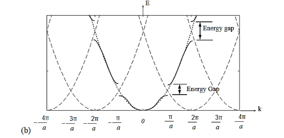
The electron energy forms quasi-continuous bands (because k itself is quasi-continuous) separated from each other by a minimum gap that occurs at ka= s(s = 0, ±1, ±2, ), or k= s/a, at which the left-hand side of Equation (21) is ±1. Figure 8(b) implies that there are multiple values of k for each E. However, the Bloch theorem says that wave functions corresponding to the wave vectors k separated by m(2/a) (since b= 0) are identical, they are the same quantum state and should be counted only once. Thus, rather than plotting the energy eigenvalues for all the wave vectors, we can plot them in one period, as shown in Figure 9. This way of representation is called the reduced-zone representation. The relationship between the energy and the wave vector is the dispersion relation.
|
Figure 8(a) Parabolic energy curves of a free electron in one dimension, periodically continued in reciprocal space. The periodicity in real space is a, and (b) extended zone: splitting of the energy parabola at the boundaries of the first Brillouin zone. The energy gaps are forbidden regions. The solid lines from Kronig-Penney model.
From the E-K diagram is clear that the electron has allowed energy values in the region or zone extending from k= -π/a to k= +π/a. This zone is called first Brillouin Zone. Higher zones can be defined accordingly from the graph.
|
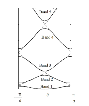
Figure 9: The solid lines show the energy bands in the reduced zone. The free electron dispersion relations are shown as dashed lines.
E-K DIAGRAM
The corresponding band structure is shown below (black curve) as well as the energy for a free electron (gray curve). Three different forms are presented, namely the E(k) diagram, the E(k diagram combined with the reduced-zone diagram as well as the reduced-zone diagram only.
|
Figure 10: Energy versus ka/π as presented in Figure (black curves) compared to that of a free electron (gray curves). Shown are: a) the E(k) diagram, b) the E(k) diagram combined with the reduced-zone diagram and c) the reduced-zone diagram only.
From Figu a we observe the following: The E(k) relation resembles a parabola except that only specific ranges of energies are valid solutions to Schrödinger's equation and therefore are allowed, while others are not. The range of energies for which there is no solution is referred to as an energy band gap. The transitions between allowed and forbidden energies occur at non-zero integer multiples of ka/ π. These correspond to local minima and maxima of the E(k) relation. The reduced-zone diagram shown in Figure 10 contains the first three bands and energy band gaps. For instance the second energy bandgap occurs between 1.5 and 2 eV, between the band maximum of the second band and the band minimum of the third band.
Key Takeaways
- The relation between the energy (through
 ) and the wave-vector, k,

- From the E-K diagram is clear that the electron has allowed energy values in the region or zone extending from k= -π/a to k= +π/a. This zone is called first Brillouin Zone.
- The E(k) relation resembles a parabola except that only specific ranges of energies are valid solutions to Schrödinger's equation and therefore are allowed, while others are not.
- The range of energies for which there is no solution is referred to as an energy band gap.
- The transitions between allowed and forbidden energies occur at non-zero integer multiples of ka/ π.
FORMATION OF ENERGY BANDS IN SOLIDS
Let us begin the conceptual path leading to the energy band model by recalling the situation inside an isolated Si atom. Ten of the 14 electrons inside an isolated Si atom are tightly bound to the nucleus and are unlikely to be significantly perturbed by normal atom—atom interactions. The remaining four electrons are rather weakly bound and, if unperturbed, occupy four of the eight allowed energy states immediately above the last core level. Moreover, it is implicitly understood that the electronic energy states within a group of Si atoms, say N Si atoms, are all identical -as long as the atoms are isolated, that is, far enough apart so that they are non-interacting.
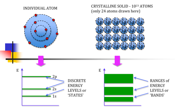
If N atoms are brought into close proximity it is quite reasonable to expect a modification in the energy states of the valence electrons. Starting with N-isolated Si atoms, and conceptually bringing the atoms closer and closer together, one finds the interatomic forces lead to a progressive spread in the allowed energies. The spread in energies gives rise to closely spaced sets of allowed-states is known as energy bands.
An isolated atom possesses discrete energies of different electrons. Suppose two isolated atoms are brought to very close, then the electrons in the orbits of two atoms interact with each other. So, that in this system, the energies of electrons will not be in the same level but changes and the energies will be slightly lower and larger than the original value. So, at the place of each energy level, a closely spaced two energy levels exists.
If ‘N’ number of atoms are brought together to form a solid and if these atoms’ electrons interact and give ‘N’ number of closely spaced energy levels in the place of discrete energy levels, it is known as bands of allowed energies. Between the bands of allowed energies, there are empty energy regions, called forbidden band of energies.
|
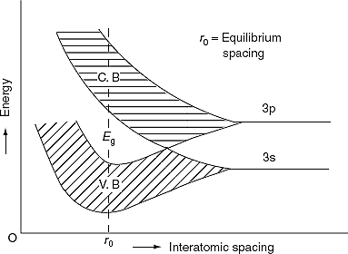
Figure 11: Formation of energy bands in solids
Kronig-Penney model shows the existence of band gap. Kronig-Penney model supports the existence of these bands of energies (allowed bands and forbidden bands).
The formation of energy bands has been explained taking Sodium (Na) metal as an example. When isolated sodium atoms are brought together to form a solid, then the energy levels of the valence electrons spread into bands. The 3S and 3P orbitals electrons energies are shown in Figure 11. These bands are seen to overlap strongly at the interatomic spacing of sodium.
We know that atoms have discrete energy levels. When a huge number of atoms are combined to form a solid, these discrete energy levels are replaced by discrete ranges of energy or called as energy bands.
In energy bands there are so many individual allowed energy values or you can say that the energy bands the energy distribution is continuous. This is shown in the following figure
|
Figure12: Energy Level and energy band
In between energy bands are ranges of energy which are entirely impossible known as band gaps
Different substances have different band structures which explain the characteristics of that substance in terms of electrical conduction.
Bands are formed by the closely spaced orbitals.
There are three types of bands:
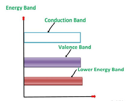
1. Valance Bands: Valence band it is a group of orbitals which contain electrons in the shell. Or we can say It is also defined as the energy band that comprises of valence electrons present in the outermost shell of an atomic structure.
These valence electrons, when provided with sufficient energy, get changed into free electrons and moves to conduction band thereby causing conductivity. It is at a lower energy level than the conduction band in the energy level diagram.
2. Conduction Band: Conduction band is a group of empty orbitals of the shells that do not contain any electron due to their configuration making the orbitals of higher energy levels.
When the electrons pass from valance band to the conduction band these solids conduct electricity with flow of charges in the form of electrons.
3. Forbidden Energy Band: These two bands are separated by a certain amount of energy known as the forbidden energy gap. In this band not a single electron is available. It diagram it is named as Band Gap.
CLASSIFICATION OF SOLIDS BASED ON BAND THEORY
Let us distinguish between conductor, semiconductors and insulator on the basis of these bands.
|
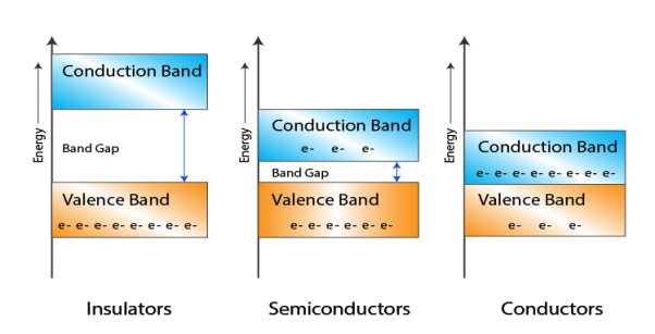
Figure 13 : Classification Of Solids Based On Band Theory
- In Conductors: The valance band and the conduction band overlap each other. This makes it easy for the electricity to pass through them. In conductors, the valence band is either not fully occupied with electrons, or the filled valence band overlaps with the empty conduction band. In general, both states occur at the same time, the electrons can therefore move inside the partially filled valence band or inside the two overlapping bands. In conductors there is no band gap between the valence band and conduction band.
- In Semi-conductors: there is a slight gap between the conduction band and the valance band. This band gap is less than or equal to 1.4 eV. The electrons from valance shell take a little energy to excite from valance band to the conduction band. Even in semiconductors, there is a band gap, but compared to insulators it is so small that even at room temperature electrons from the valence band can be lifted into the conduction band. The electrons can move freely and act as charge carriers.
- In Insulators: In insulators the valence band is fully occupied with electrons due to the covalent bonds. To achieve conductivity, electrons from the valence band have to move into the conduction band. the energy gap is considerably large and the electrons of the valance band cannot be excited to the conduction band before the melting or the dissociation of the solid. This means that under the practically ambient condition it cannot conduct electricity.
Key Takeaways
- Energy Bond Model gives the energy aspect of atoms to get good knowledge of semiconductor.
- The spread in energies gives rise to closely spaced sets of allowed-states is known as energy bands.
- Bands are formed by the closely spaced orbitals.
- There are three types of bands: Valence band, conduction band, Forbidden Energy Band
- The Valence band and conduction band are separated by a certain amount of energy known as the forbidden energy gap.
- Insulators are those having wide band gap.
- Metals: very small or no band gap exists at all due to an overlap of the valence and conduction bands
- Semiconductors is an intermediate case
- On the basis of band theory we can classify the materials as conductors, semiconductors, and insulators based on these bands.
Semiconductors
Semiconductors are materials that have conductivity between conductors and insulators.
Semiconductors can be pure elements, such as silicon or germanium, or compounds such as gallium arsenide or cadmium selenide.
They are not good conductors nor good insulators as their name “semi”-conductors.
These materials such as silicon (Si), germanium (Ge), and gallium arsenide (GaAs), have electrical properties somewhere in the middle, between those of a “conductor” and an “insulator”.
They have very few “free electrons” because their atoms are closely grouped in a crystalline pattern called a “crystal lattice” but electrons are still able to flow, but only under special conditions.
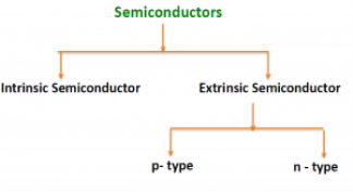
There are two basic groups or classifications that can be used to define the different semiconductor types:
- Intrinsic Semiconductor
- Extrinsic Semiconductor
|
Figure 14: Type of semiconductor
The semiconductor is divided into two types. One is an Intrinsic Semiconductor and the other is an Extrinsic semiconductor. The pure form of the semiconductor is known as the intrinsic semiconductor and the semiconductor in which intentional impurities are added for making it conductive is known as the extrinsic semiconductor.
The conductivity of the intrinsic semiconductor becomes zero at room temperature while the extrinsic semiconductor is very little conductive at room temperature. The detailed explanation of the two types of the semiconductor is given below.
INTRINSIC SEMICONDUCTOR
An intrinsic type of semiconductor material made to be very pure chemically. As a result, it possesses a very low conductivity level having very few charge carriers, namely holes and electrons, which it possesses in equal quantities.
|
Figure 15: Intrinsic Semiconductor
The most commonly used semiconductor basics material by far is silicon. Silicon has four valence electrons in its outermost shell which it shares with its neighbouring silicon atoms to form a full orbital of eight electrons. The structure of the bond between the two silicon atoms is such that each atom shares one electron with its neighbour making the bond very stable.
As there are very few free electrons available to move around the silicon crystal, crystals of pure silicon (or germanium) are therefore good insulators. Silicon atoms are arranged in a definite symmetrical pattern making them a crystalline solid structure. A crystal of pure silica (silicon dioxide or glass) is generally said to be an intrinsic crystal (it has no impurities) and therefore has no free electrons.
An extremely pure semiconductor is called an Intrinsic Semiconductor. Based on the energy band phenomenon, an intrinsic semiconductor at absolute zero temperature is shown below.
|
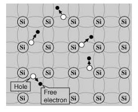
Figure 16: Intrinsic semiconductor at absolute zero temperature.
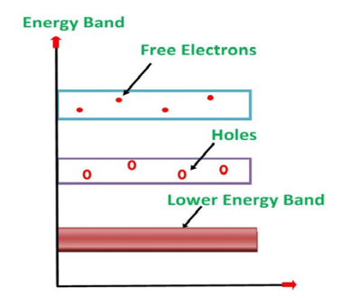
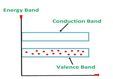
Its valence band is filled and the conduction band is empty. When the temperature is raised and some heat energy is supplied to it, some of the valence electrons are lifted to the conduction band leaving behind holes in the valence band as shown below.
|
Figure 17: Intrinsic semiconductor at T >0
A hole is the absence of an electron in a particular place in an atom. Although it is not a physical particle in the same sense as an electron, a hole can be passed from atom to atom in a semiconductor material. It is considered to have a positive charge. Holes are positive charge carriers.
The electrons reaching the conduction band move randomly. The holes created in the crystal also free to move anywhere.
This behaviour of the semiconductor shows that they have a negative temperature coefficient of resistance. This means that with the increase in temperature, the resistivity of the material decreases, and the conductivity increases.
But simply connecting a silicon crystal to a battery supply is not enough to extract an electric current from it. To do that we need to create a “positive” and a “negative” pole within the silicon allowing electrons and therefore electric current to flow out of the silicon. These poles are created by doping the silicon with certain impurities.
The process by which an impurity is added to a semiconductor is known as Doping. The amount and type of impurity which is to be added to the material have to be closely controlled during the preparation of extrinsic semiconductor. Generally, one impurity atom is added to 108 atoms of a semiconductor.
The purpose of adding impurity in the semiconductor crystal is to increase the number of free electrons or holes to make it conductive.
If a Pentavalent impurity, having five valence electrons is added to a pure semiconductor a large number of free electrons will exist. Which makes an n-type extrinsic semiconductor.
If a trivalent impurity having three valence electrons is added, a large number of holes will exist in the semiconductor. Which makes a p-type extrinsic semiconductor.
EXTRINSIC SEMICONDUCTOR
Extrinsic types of semiconductors are those where a small amount of impurity has been added to the basic intrinsic material. This 'doping' uses an element from a different periodic table group and in this way, it will either have more or fewer electrons in the valence band than the semiconductor itself. This creates either an excess or shortage of electrons. In this way two types of semiconductors are available: Electrons are negatively charged carriers. Holes are positively charged carriers.
Depending upon the type of impurity added the extrinsic semiconductor may be classified as an n-type semiconductor and p-type semiconductor.
P-TYPE EXTRINSIC SEMICONDUCTOR
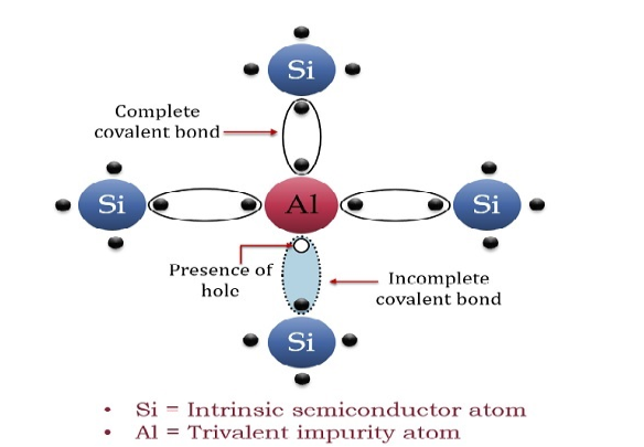
The extrinsic p-Type Semiconductor is formed when a trivalent impurity is added to a pure semiconductor in a small amount, and as a result, a large number of holes are created in it. A large number of holes are provided in the semiconductor material by the addition of trivalent impurities like Gallium and Indium. Such type of impurities which produce a p-type semiconductor is known as an Acceptor Impurities because each atom of them creates one hole which can accept one electron.
In a P-type semiconductor material, there is a shortage of electrons, i.e. there are 'holes' in the crystal lattice. Electrons may move from one empty position to another and in this case, it can be considered that the holes are moving. This can happen under the influence of a potential difference and the holes can be seen to flow in one direction resulting in an electric current flow. It is harder for holes to move than for free electrons to move and therefore the mobility of holes is less than that of free electrons. Holes are positively charged carriers.
A trivalent impurity like Aluminium, having three valence electrons is added to Silicon crystal in a small amount. Each atom of the impurity fits in the Silicon crystal in such a way that its three valence electrons form covalent bonds with the three surrounding Silicon atoms as shown in the figure below.
|
Figure 18: p-Type Semiconductor
ENERGY BAND DIAGRAM OF P-TYPE SEMICONDUCTOR
The energy band diagram of a p-Type Semiconductor is shown below.
|
Figure 19: Energy band diagram of a p-Type Semiconductor
A large number of holes or vacant space in the covalent bond is created in the crystal with the addition of the trivalent impurity. A small or minute quantity of free electrons is also available in the conduction band.
They are produced when thermal energy at room temperature is imparted to the Silicon crystal-forming electron-hole pairs. But the holes are more in number as compared to the electrons in the conduction band. It is because of the predominance of holes over electrons that the material is called a p-type semiconductor. The word “p” stands for positive material.
CONDUCTION THROUGH P TYPE SEMICONDUCTOR
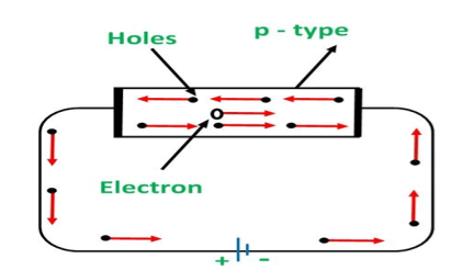
In p-type semiconductors, a large number of holes are created by the trivalent impurity. When a potential difference is applied across this type of semiconductors.
|
Figure 20: Conduction through p type semiconductor
The holes are available in the valence band are directed towards the negative terminal. As the current flow through the crystal is by holes, which are a carrier of positive charge, therefore, this type of conductivity is known as positive or p-type conductivity. In a p-type conductivity, the valence electrons move from one covalent to another.
The conductivity of an n-type semiconductor is nearly double that of a p-type semiconductor. The electrons available in the conduction band of the n-type semiconductor are much more movable than holes available in the valence band in a p-type semiconductor. The mobility of holes is poor as they are more bound to the nucleus.
Even at room temperature, the electron-hole pairs are formed. These free electrons which are available in minute quantity also carry a little amount of current in the p-type semiconductors.
N-TYPE EXTRINSIC SEMICONDUCTOR
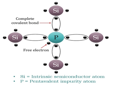
When a few Pentavalent impurities such as Phosphorus whose atomic number is 15, which is categorized as 2, 8, and 5. It has five valence electrons, which are added to silicon crystals. Each atom of the impurity fits in four silicon atoms as shown in the figure below.
Hence, each Arsenic atom provides one free electron in Silicon crystal. Since an extremely small amount of Phosphorus, impurity has a large number of atoms; it provides millions of free electrons for conduction.
|
Figure 21: N-type semiconductor
An N-type semiconductor material has an excess of electrons. In this way, free electrons are available within the lattices, and their overall movement in one direction under the influence of a potential difference results in an electric current flow. This is an N-type semiconductor, the charge carriers are electrons.
ENERGY DIAGRAM OF N-TYPE SEMICONDUCTOR
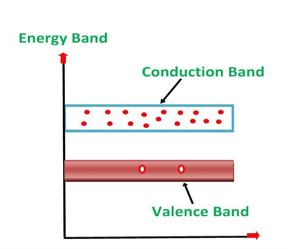
A large number of free electrons are available in the conduction band because of the addition of the Pentavalent impurity. These electrons are free electrons that did not fit in the covalent bonds of the crystal. However, a minute quantity of free electrons is available in the conduction band forming hole- electron pairs.
The Energy diagram of the n-type semiconductor is shown in the figure below.
|
Figure 22: Energy diagram of the n-type semiconductor
- The addition of pentavalent impurity results in a large number of free electrons.
- When thermal energy at room temperature is imparted to the semiconductor, a hole-electron pair is generated and as a result, a minute quantity of free electrons is available. These electrons leave behind holes in the valence band.
- Here n stands for negative material as the number of free electrons provided by the pentavalent impurity is greater than the number of holes.
CONDUCTION THROUGH N-TYPE SEMICONDUCTOR
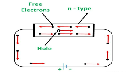
In the n-type semiconductor, a large number of free electrons are available in the conduction bands which are donated by the impurity atoms. The figure below shows the conduction process of an n-type semiconductor.
When a potential difference is applied across this type of semiconductor, the free electrons are directed towards the positive terminals. It carries an electric current. As the flow of current through the crystal is constituted by free electrons which are carriers of a negative charge, therefore, this type of conductivity is known as negative or n-type conductivity.
|
Figure 23: Conduction through n-type semiconductor
The electron-hole pairs are formed at room temperature. These holes which are available in small quantities in the valence band also consist of a small amount of current. For practical purposes, this current is neglected.
Key Takeaways
- Semiconductors are materials that have conductivity between conductors and insulators.
- The semiconductor is divided into two types. One is an Intrinsic Semiconductor and the other is an Extrinsic semiconductor.
- The pure form of the semiconductor is known as the intrinsic semiconductor
- The semiconductor in which intentional impurities are added for making it conductive is known as the extrinsic semiconductor.
- A hole is the absence of an electron in a particular place in an atom.
- The process by which an impurity is added to a semiconductor is known as Doping.
- Depending upon the type of impurity added the extrinsic semiconductor may be classified as an n-type semiconductor and p-type semiconductor.
- The extrinsic p-Type Semiconductor is formed when a trivalent impurity is added to a pure semiconductor in a small amount, and as a result, a large number of holes are created in it.
- The extrinsic n-Type Semiconductor is formed when a Pentavalent impurity is added to a pure semiconductor in a small amount, and as a result, a large number of electrons are created in it.
FERMI ENERGY
Intrinsic semiconductors—carrier concentration
Here we will calculate the number of electrons excited into the conduction band at temperature T and also the hole concentration in the valence band. It is assumed that the electrons in the conduction band behave as if they are free particles with effective mass me* and the holes near the top of the valence band behave as if they are free particles with effective mass mh*.
Here we will calculate the electron concentration, hole concentration
The density of Electrons in Conduction Band
The number of free electrons per unit volume of a semiconductor having energies in between E and E + dE is represented as N(E) dE dE = width of Energy band Therefore, we have: N(E) dE = ge(E) dE fe(E) ……….(1) ge(E) = The density of electron states per unit volume fe(E) = Fermi-Dirac distribution function i.e. probability that an electron occupies an electron state The number of electrons present in the conduction band per unit volume of material ‘n’ is obtained by integrating N(E) dE between the limits Ec and Ect Where Ec = the bottom energy levels of the conduction band Ect = the bottom and top energy levels of the conduction band n = can be written as n = n = we know that above Ect, there are no electrons. Hence, Equation (3) becomes n = n = The Fermi-Dirac distribution function fe(E) can be represented as:
Compared to the exponential value, so the ‘1’ in the denominator can be neglected. So Hence, The density of electron states ge(E) in the energy space from E = 0 to E can be written as:
where me* is the effective mass of an electron and h is Planck’s constant.
To evaluate n, the density of states is counted from Ec, since the minimum energy state in the conduction band is Ec. so eq (8) can become
Substituting Equations (6) and (9) in (4) gives n = n = The above equation can be simplified by the following substitution: Put ɛ = E − Ec ………… (11) So, dɛ = dE In Equation (11), Ec is constant, as we change the variable E to ε in Equation (10), the integral limits also change. In Equation (11), as E → Ec then ε → 0 and E → ∞, then ε also → ∞. the exponential term in Equation (10) becomes:
Substituting Equations (11) and (12) in (10), we get: n = n = Above integral (I) can be simplified by substitution. Put ε = x2 so that dɛ = 2x dx I = = = Substituting Equation (14) in (13) gives: n = n = n = n = The term n =Nc
The density of Holes in Valence Band The number of holes per unit volume of semiconductor in the energy range E and E + dE in the valence band is represented as P(E) dE. Proceeding the same way (as in the case of electrons) we have Therefore, we have: P(E) dE = gh(E) dE fh(E) ……….(17) dE = width of Energy band gh(E) = The density of holes states per unit volume fh(E) = Fermi-Dirac distribution function i.e. probability that a hole occupies an electron state The number of electrons present in the conduction band per unit volume of material ‘n’ is obtained by integrating P(E) dE between the limits Evb and EV where EV = the bottom energy levels of the valence band Evb = the bottom and top energy levels of the valence band The total number of holes present in the valence band per unit volume of material ‘p’ is obtained by integrating P(E) dE
Equation (18) can be represented as:
Now we know that below Evb no holes are present. Hence, Equation (19) becomes
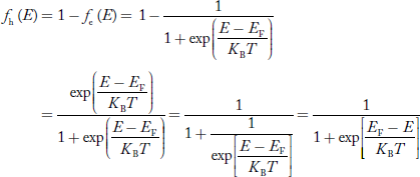
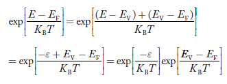
We know a hole can also be defined as the absence of an electron. presence of a hole = the absence of an electron Hence, the Fermi-Dirac function of holes fh(E) in the valence band is:
Compared to exponential, the ‘1’ in the denominator is negligible, Hence,
The density of hole states between E and E + dE in valence band can be written similar to Equation (8.9) for electrons.
Where mh* is the effective mass of the hole. Substituting Equations (21) and (22) in (20),
The above equation can be simplified by the substitution: Put ɛ = EV − E ............. (24) so dɛ = − dE In Equation (24), EV is constant, as we change the variable E to ε in Equation (23), the integral limits also change. In Equation (24), as E → EV then ε → 0 and E→ −∞, then ε → ∞ the exponential term in Equation (23) becomes:
Substituting Equations (24) and (25) in (23), we get:
From Equation (14), we know the integral value
….The term
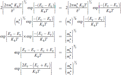
Fermi Level We know that in an intrinsic semiconductor Electron concentration ‘n’ = Hole concentration ‘p’ Equating Equations (15) and (27), we get
Taking logarithms on both sides, we get
Normally, mh* is greater than me*, since ln Temperature effect on Fermi level Fermi level slightly rises with an increase of temperature. But in the case of a pure intrinsic semiconductor like Si and Ge, mh* ≈ me* So in these cases, the Fermi level lies in the middle of the energy gap.
|
Key Takeaways
- The density of Electrons in Conduction Band
n =Nc
- The density of Holes in Valence Band

- Fermi level slightly rises with an increase of temperature. But in the case of a pure intrinsic semiconductor like Si and Ge, mh* ≈ me*, So in these cases, the Fermi level lies in the middle of the energy gap.
A P-N Junction Diode is formed by doping one side of a piece of silicon with a P-type dopant (Boron) and the other side with a N-type dopant (phosphorus). Ge can be used instead of Silicon. The P-N junction diode is a two-terminal device. This is the basic construction of the P-N junction diode. It is one of the simplest semiconductor devices as it allows current to flow in only one direction.
ZERO BIASED CONDITION
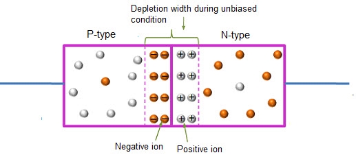
In this case, no external voltage is applied to the P-N junction diode; and therefore, the electrons diffuse to the P-side and simultaneously holes diffuse towards the N-side through the junction, and then combine with each other. Due to this an electric field is generated by these charge carriers. The electric field opposes further diffusion of charged carriers so that there is no movement in the middle region. This region is known as depletion width or space charge.
|
Figure 24: Unbiased or zero biased PN Junction Diode
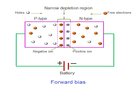
In the forward bias condition, the positive terminal of the battery is connected to the P-Type material and the negative terminal of the battery is connected to the N-type material. This connection is also called as giving positive voltage.
|
Figure 25: Forward bias
Electrons from the N-region cross the junction and enters the P-region. Due to the attractive force that is generated in the P-region the electrons are attracted and move towards the positive terminal. Simultaneously the holes are attracted to the negative terminal of the battery. By the movement of electrons and holes current flows. In this condition, the width of the depletion region decreases due to the reduction in the number of positive and negative ions.
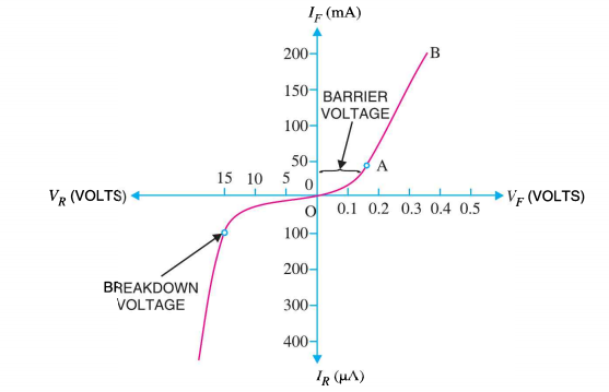
If this external voltage Vf becomes greater than the value of the potential barrier, approx. 0.7 volts for silicon and 0.3 volts for germanium, the potential barriers opposition will be overcome and current will start to flow.
This is because the negative voltage pushes or repels electrons towards the junction giving them the energy to cross over and combine with the holes being pushed in the opposite direction towards the junction by the positive voltage. This results in a characteristics curve of zero current flowing up to this voltage point, called the “knee” on the static curves and then a high current flow through the diode with little increase in the external voltage as shown in I-V characteristics.
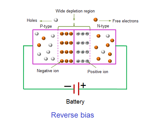
In the reverse bias condition, the negative terminal of the battery is connected to the P-type material and the positive terminal of the battery is connected to the N-type material. This connection is also known as giving negative voltage.
|
Figure 26: Reverse bias
The positive voltage applied to the N-type material attracts electrons towards the positive electrode and away from the junction, while the holes in the P-type end are also attracted away from the junction towards the negative electrode.
The net result is that the depletion layer grows wider due to a lack of electrons and holes and presents a high impedance path, almost an insulator. The result is that a high potential barrier is created thus preventing current from flowing through the semiconductor material.
This condition represents a high resistance value to the PN junction and practically zero current flows through the junction diode with an increase in bias voltage. However, a very small leakage current does flow through the junction which can be measured in micro-amperes, ( μA ).
If the reverse bias voltage Vr applied to the diode is increased to a sufficiently high enough value, it will cause the diode’s PN junction to overheat and fail due to the avalanche effect around the junction. This may cause the diode to become shorted and will result in the flow of maximum circuit current, and this shown as a step downward slope in the reverse static characteristics curve in I-V characteristics.
I-V CHARACTERISTICS OF PN JUNCTION DIODE
The I-V Characteristic Curves, which is short for Current-Voltage Characteristic Curves or simply I-V curves of an electrical device
The application of a forward biasing voltage on the junction diode results in the depletion layer becoming very thin and narrow which represents a low impedance path through the junction thereby allowing high currents to flow. The point at which this sudden increase in current takes place is represented on the static I-V characteristics curve above as the “knee” point. The current starts increasing with increase in voltage. At knee voltage current shows a sharp increment in its magnitude. This behaviour is mentioned above. As large current flow in forward biasing so we measure this current in mA.
When a junction diode is Reverse Biased, the thickness of the depletion region increases and the diode acts like an open circuit blocking current flow. So only a very small leakage current will flow.
|
Figure 27: I-V characteristics
Note in addition that the minority carrier drift currents are not affected by the height of the potential bill. It is the number of minority carriers wandering into the depletion region per second that determines the current flow.
The situation is similar to a waterfall. The water flowing over the falls is independent of the height of the falls. the overall 1-V dependence is concluded to be of the general form 1-V chracteristics.
 ………..(1)
Equation (1) is identical to the ideal diode equation if VA is set equal to kT/q.
Key Takeaways
- A P-N Junction Diode is formed by doping one side of a piece of silicon with a P-type dopant (Boron) and the other side with a N-type dopant (phosphorus). Ge can be used instead of Silicon.
- Zero biased condition is the case when no external voltage is applied to the P-N junction diode.
- In the forward bias condition, the positive terminal of the battery is connected to the P-Type material and the negative terminal of the battery is connected to the N-type material. This connection is also called as giving positive voltage.
- In the reverse bias condition, the negative terminal of the battery is connected to the P-type material and the positive terminal of the battery is connected to the N-type material. This connection is also known as giving negative voltage.
A thermistor is a resistance thermometer, or a resistor whose resistance is dependent on temperature. The term is a combination of “thermal” and “resistor”.
Thermistor is special type of resistor, whose resistance varies more significantly with temperature than in standard resistors. Generally, the resistance increases with the temperature for most of the metals but the thermistors respond negatively i.e. the resistance of the thermistors decrease with the increase in temperature. This is the basic principle behind thermistor. As the resistance of thermistors depends on the temperature, they can be connected in the electrical circuit to measure the temperature of the body.
There are two types of thermistors:
- Negative Temperature Coefficient (NTC)
- Positive Temperature Coefficient (PTC)
Negative Temperature Coefficient (NTC): When the temperature increases, resistance decreases. Conversely, when temperature decreases, resistance increases. This type of thermistor is used the most.
Many NTC thermistors are made from a pressed disc or cast chip of a semiconductor. They work because raising the temperature of a semiconductor increases the number of electrons able to move about and carry charge – it promotes them into the conduction band. The more charge carriers that are available, the more current a material can conduct. This is given by the formula:
I = n.A.v.e
Where\
I = electric current (amperes)
n = density of charge carriers (count/m³)
A = cross-sectional area of the material (m²)
v = velocity of charge carriers (m/s)
e = charge of an electron
The current is measured using an ammeter. Over large changes in temperature, calibration is necessary. Over small changes in temperature, if the right semiconductor is used, the resistance of the material is linearly proportional to the temperature. There are many different semiconducting thermistors with a range from about 0.01 kelvin to 2,000 kelvins (-273.14 °C to 1,700 °C)
NTC thermistors are used as current-limiters and temperature monitors in digital thermostats and automobiles.
Positive Temperature Coefficient (PTC)
A PTC thermistor works a little differently. When temperature increases, the resistance increases, and when temperature decreases, resistance decreases. The relationship between resistance and temperature is linear, as expressed in the following equation:  R = k
R = k T
T
Where  R = change in resistance
 T = change in temperature
k = temperature coefficient.
When k is positive, it causes a linear increase in resistance as the temperature rises. This type of thermistor is generally used as a fuse. When the circuit heats up, resistance increases to prevent overload.
They are also used as timing devices in televisions. When the unit is switched on, the degaussing coil is activated to eliminate the magnetic field; the thermistor automatically switches it off when the temperature reaches a certain point.
Thermistor characteristics:
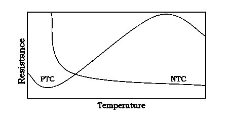
As discussed, resistance increase with increase in temperature for PTC and resistance decrease with increase in temperature for NTC.
The thermistor exhibits a highly non-linear characteristic of resistance vs temperature.
|
Figure 28: PTC Vs NTC
PTC thermistors can be used as heating elements in small temperature controlled ovens. NTC thermistors can be used as inrush current limiting devices in power supply circuits. Inrush current refers to maximum, instantaneous input current drawn by an electrical device when first turned on. Thermistors are available in variety of sizes and shapes; smallest in size are the beads with a diameter of 0.15mm to 1.25mm.
There are two fundamental ways to change the temperature of thermistor internally or externally. The temperature of thermistor can be changed externally by changing the temperature of surrounding media and internally by self-heating resulting from a current flowing through the device.
The dependence of the resistance on temperature can be approximated by
following equation,
R = R0  …………….(1)
Where,
R is the resistance of thermistor at the temperature T (in K)
R0 is the resistance at given temperature T0 (in K)
β is the material specific-constant
The material specific-constant of a NTC thermistor is a measure of its resistance at one temperature compared to its resistance at a different temperature. Its value may be calculated by the formula shown below and is expressed in degrees Kelvin (°K).
Differentiating (1) w.r.t to T, we get
 =
= 
 =
=  is the temperature coefficient of resistance
Taking log of (1) and simplifying we get
 =
=  …………..(2)
So
 =
=  …………..(3)
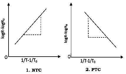
A graph plotted between  and
and  in x-axis for NTC and PTC is shown below. The slope of the graph gives the value of
|
Figure 29: NTC - PTC Characteristics
THERMISTOR APPLICATIONS
- PTC thermistors were used as timers in the degaussing coil circuit of most CRT displays.
- We can also use PTC thermistors as heater in automotive industry to provide additional heat inside cabin with diesel engine or to heat diesel in cold climatic conditions before engine injection.
- We can use PTC thermistors as current-limiting devices for circuit protection, as replacements for fuses.
- We can also use NTC thermistors to monitor the temperature of an incubator.
- Thermistors are also commonly used in modern digital thermostats and to monitor the temperature of battery packs while charging.
- We regularly use NTC thermistors in automotive applications.
- NTC thermistors are used in the Food Handling and Processing industry, especially for food storage systems and food preparation. Maintaining the correct temperature is critical to prevent food borne illness.
- NTC thermistors are used throughout the Consumer Appliance industry for measuring temperature. Toasters, coffee makers, refrigerators, freezers, hair dryers, etc. all rely on thermistors for proper temperature control.
- We can regularly use the Thermistors in the hot ends of 3D printers; they monitor the heat produced and allow the printer’s control circuitry to keep a constant temperature for melting the plastic filament.
- NTC thermistors are used as resistance thermometers in low-temperature measurements of the order of 10 K.
- NTC thermistors can be used as inrush-current limiting devices in power supply circuits.
Key Takeaways
- A thermistor is a resistance thermometer, or a resistor whose resistance is dependent on temperature. The term is a combination of “thermal” and “resistor”.
- There are two types of thermistors: Negative Temperature Coefficient (NTC) and Positive Temperature Coefficient (PTC)
- Negative Temperature Coefficient (NTC): When the temperature increases, resistance decreases. Conversely, when temperature decreases, resistance increases. This type of thermistor is used the most.
- A PTC thermistor works a little differently. When temperature increases, the resistance increases, and when temperature decreases, resistance decreases.
When the magnetic field is applied perpendicular to a current-carrying conductor, then a voltage is developed in the material perpendicular to both the magnetic field and current in the conductor. This effect is known as Hall Effect and the voltage developed is known as Hall voltage (VH).
Hall Effect is useful to identify the nature of charge carriers in material and hence to decide whether the material is an n-type semiconductor or p-type semiconductor, also to calculate carrier concentration and mobility of carriers.
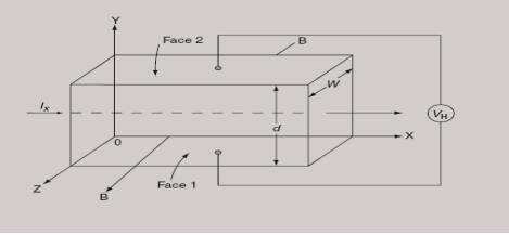
Hall Effect can be explained by considering a rectangular block of an extrinsic semiconductor in which current is flowing along the positive X-direction and magnetic field B is applied along Z-direction as shown in Figure.
|
Figure 30: Hall Effect
Suppose if the semiconductor is n-type, then mostly the carriers are electrons and the electric current is due to the drifting of electrons along negative X-direction or if the semiconductor is p-type, then mostly the carriers are holes and the electric current is due to drifting of the holes along positive X-direction.
As these carriers are moving in the magnetic field in the semiconductor that means they experience Lorentz force represented by FL
FL = Bevd
Where vd is the drift velocity of the carriers. (already explained in the previous section).
We can obtain the direction of this force by applying Fleming’s left-hand rule in electromagnetism.
Fleming’s left-hand rule can be explained as If we stretch the thumb, forefinger, and middle finger in three perpendicular directions so that the forefinger is parallel to the magnetic field and the middle finger is parallel to the current direction, then the thumb represents the direction of the force on the current-carrying carriers.
So the Lorentz force is exerted on the carriers in the negative Y-direction. Due to Lorentz force, more and more carriers will be deposited at the bottom face (represented by face 1in the figure) of the conductor.
The deposition of carriers at the bottom face is continued till the repulsive force due to accumulated charge balances the Lorentz force.
After some time of the applied voltage, both the forces become equal in magnitude and act in opposite direction, then the potential difference between the top and bottom faces is equal to Hall voltage and that can be measured.
At equilibrium, the Lorentz force on a carrier FL = Bevd ……………..(1) and the Hall force FH = eEH ……………..(2) Where EH is the Hall electric field due to accumulated charge. At equilibrium, FH = FL eEH = Bevd ∴ EH = Bvd ……………..(3) If ‘d’ is the distance between the upper and lower surfaces of the slab, then the Hall field EH = In n-type material, Jx = –nevd vd = - Where n is free electron concentration, substituting (5) in (3), we have ∴ EH = -B For a given semiconductor, the Hall field EH is proportional to the current density Jx and the intensity of magnetic field ‘B’ in the material. i.e. EH ∝ JxB (or) EH = RHJxB ……………..(7) Where RH = Hall coefficient Equations (6) and (7) are the same so, we have RHJxB =-B RH = - Where ρ is the charge density Similarly for p-type material RH = Using Equations (8) and (9), carrier concentration can be determined. Thus, the Hall coefficient is negative for n-type material. In n-type material, as the more negative charge is deposited at the bottom surface, so the top face acquires positive polarity and the Hall field is along negative Y-direction. The polarity at the top and bottom faces can be measured by applying probes. Similarly, in the case of p-type material, a more positive charge is deposited at the bottom surface. So, the top face acquires negative polarity and the Hall field is along positive Y-direction. Thus, the sign of the Hall coefficient decides the nature of (n-type or p-type) material. The Hall coefficient can be determined experimentally in the following way: Multiplying Equation (7) with ‘d’, we have EHd = VH = RHJxBd ……………..(10) From (Figure 30) we know the current density Jx Jx = Where W is the width of the box. Then, Equation (10) becomes VH = RH RH = Substituting the measured values of VH, Ix, B, and W in Equation(11), RH is obtained. The polarity of VH will be the opposite for n- and p-type semiconductors. The mobility of charge carriers can be found by using the Hall effect, for example, the conductivity of electrons is n = neμn Or we can rewrite it as μn = by using equation (11) μn = n
|
• Using magnetic flux leakage – To properly inspect items such as pipes or tubes, Hall Effect probes work with something called magnetic flux leakage. This is a way of testing such items, and being able to spot potential corrosion, erosion, or pitting. This is specifically used in steel items and can give important information about lifespan or safety.
• Sensors to detect rotation speed – A Hall Effect probe can be used in bicycle wheels, speedometers in the automotive world, electronic types of ignition systems, and gear teeth.
• Used to detected movement – You will often find a Hall Effect probe used in such items as Go-Kart controls, smartphones, paintball guns, or airsoft guns, as well as some GPS systems.
• Ferrite Toroid Hall Effect current transducers – This is mainly used in electronic compasses, making use of the magnetic field to show direction.
• Split-ring clamp-on sensors – These types of Hall Effect probes are used to test equipment without having to take the whole circuit board apart, e.g. complex items.
• Analog multiplication – Anything which needs a power measurement, e.g. sensing, and is also used in small computers.
• General power measurement – Any device which needs to be tested for its power input can be done by a Hall Effect probe.
• Position and motion sensors – This is mainly used in a DC motor, often the brushless type.
• The automotive world – Hall Effect probes are used widely in the automotive world, especially in fuel injection and ignition. Wheel rotation sensors also use Hall Effect probes, e.g. for anti-lock braking.
- For determination of the type of given semiconductor.
- For N-type, Hall coefficient RH= negative
- For P-type, Hall coefficient RH= Positive
- To determine carrier concentration n and p; that is n=p=1/e𝑅𝐻
- Determination of mobility of charge carriers μn =
 =n RH. Where 𝜎= electrical conductivity
 - To determine the sign of charge carriers whether the conductivity is due to electrons or holes.
Main Advantages of Using Hall Sensors
Why is a Hall Effect probe advantageous in all of these instances? Because the probes are not affected by outside influences, e.g. water or dirt. They can also easily sense the measure of the output they need when they are placed in the right position. On top of this, Hall Effect probes are safer, because the voltage never actually makes it directly to the sensor/probe. This makes this type of measurement overall so much safer than other methods.
As you can see, understanding how something is put into practice in the real world helps you to understand it in real terms. The Hall Effect is certainly very commonplace these days, in much more methods and applications than we realize. While certainly very useful in the automation world, even basic items such as a compass make large use of this scientific approach.
Key Takeaways
- When the magnetic field is applied perpendicular to a current-carrying conductor, then a voltage is developed in the material perpendicular to both the magnetic field and current in the conductor. This effect is known as Hall Effect.
- The voltage developed is known as Hall voltage (VH).
- Hall Effect is useful to identify the nature of charge carriers in material and hence to decide whether the material is an n-type semiconductor or p-type semiconductor.
- Hall Effect also to calculate carrier concentration and mobility of carriers.
- Hall coefficient is given by RH = -
 = -
= -  Where ρ is the charge density
 - Hall coefficient is given by RH =

- Mobility of charge carriers can be found by using the Hall Effect μn = n

Definitions:
A dielectric is an electrical insulator that can be polarized by an applied electric field. Or
A dielectric is non-conducting material which stores electrical charges.
In other words, A material that does not conduct electricity but on applying electric field, induced charges produced on its faces. Such an insulator is called Dielectric.
Dielectrics are insulators i.e. non-conducting substances which are bad conductor of electric current. Dielectric materials can stores an electrostatic charge while dissipating minimal energy in the form of heat.
Examples of dielectric are Mica, Plastics, Glass, Porcelain and Various Metal Oxides and even dry air is also example of dielectric. The dielectric constant of a vacuum is, of course, unity.
Classification of Dielectric
The response of a dielectric material depends on the nature of its molecules. The molecules of a dielectric is of two types
- Polar molecules
- Non polar molecules
Polar Molecules: Polar Molecules are those in which centre of gravity of positive and negative charge does not coincide with each other. This is because they all are asymmetric in shape. Examples: H2O, CO2, NO2 etc. The molecule of material are composed of two or more different atoms, which have permanently dipole moment because the centre of gravity of positive charge and negative charge does not coincide with each other but separated by a finite (small) distance.
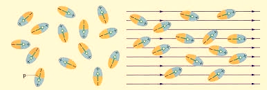
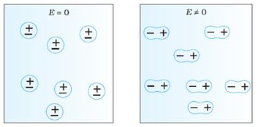
Normally this type of molecular dipole in polar dielectric are randomly oriented such that their net dipole moment becomes zero and material act as a neutral material.
|
Figure 31: Effect of electric felid on dielectric
Polar Molecules are those type of dielectric in which the possibilities that the positive and negative molecules will coincide with each other is null or zero.
Non-Polar Molecule: Non-polar molecules are those in which centre of gravity of positive charge and negative charge coincide with each other. The molecule has zero dipole moment as they all are symmetric in shape. Examples: O2, N2, H2 etc.
Dielectrics materials in which the molecule's center of gravity of positive charge and negative charge coincide with each other and so the molecules are electrically neutral and hence zero dipole moment.
|
Figure 32: Polar molecules & Non polar molecules
Difference between Dielectric and Insulators
Dielectrics are often confused with insulators. Here are some points of differences
- Dielectric is the material which stores the electrical energy in an electric field whereas insulator is that material which blocks the flow of electrons.
- Dielectric material is polarised whereas insulator material doesn’t get polarised.
- Molecules in dielectric are weakly bounded as compared to molecules in insulator.
- Dielectric material has high dielectric constant whereas insulator has low dielectric constant.
- Examples of Dielectric material are dry air, vacuum, Glass, Porcelain, Various Metal Oxides and distilled water. Whereas Examples of insulator are cotton, plastic, rubber etc.
In dielectric material molecules are tightly bounded to the nucleus and not able to move freely as in case of conductor. But when a dielectric material is placed in an electric field, electric charges do not flow through the material as they flow in case of an electrical conductor but only slightly shift from their average equilibrium positions causing dielectric polarization. Because of dielectric polarization, positive charges are displaced in the direction of the field and negative charges shift in the direction opposite to the field. In dielectric molecules are tightly bound to the nucleus and not able to move freely as in case of conductors. The dielectric material is largely used in the manufacturing of capacitor.
Response of Dielectric to External Electric Field
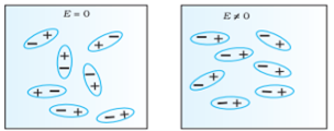
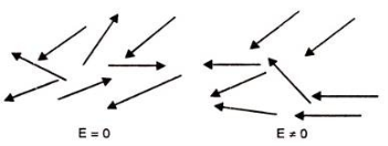
In case of Polar Molecules -When the electric field is not present, it causes the electric dipole moment of these molecules in a random direction. This is why the average dipole moment is zero. If the external electric field is present, the molecules align themselves in the direction electric field and resulted in having dipole moment.
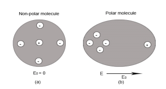
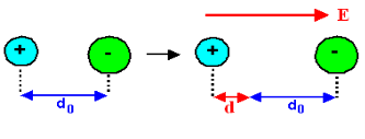
In case of Non-Polar Molecules – As we know nonpolar molecule has zero dipole moment. In spite of zero dipole, when a dielectric nonpolar material is placed in an electric field. The positive and the negative charges in a nonpolar molecule experience forces in opposite directions. This force causes the separation between the charges and hence nonpolar molecule experiences induced dipole moment.
|
Figure 33 (a) (left) Non Polar Molecule (b) (right) Polar Molecule
Key Takeaways
- A dielectric is non-conducting material which stores electrical charges.
- Examples of dielectric are Mica, Plastics, Glass, Porcelain and Various Metal Oxides and even dry air is also example of dielectric.
- The molecules of a dielectric is of two types Polar molecules and Non-polar molecules
- Polar Molecules are those in which centre of gravity of positive and negative charge does not coincide with each other.
- Non-polar molecules are those in which centre of gravity of positive charge and negative charge coincide with each other. The molecule has zero dipole moment as they all are symmetric in shape.
- In the presence of electric field molecules gets polarized.
"When a dielectric material placed in external electrical field, it's molecule gain electric dipole moment and dielectric said to be polarised"
"The induce moment per unit volume of dielectric material is called the electric polarization of dielectric." It is represented by vector p.
Type of dielectric polarization
There are four types of dielectric polarization
1. Electronic polarization
2. Ionic polarization
3. Orientational polarization
4. Space charge polarization
1. Electric Polarization
Electronic polarization refers to the separation of centre of positive charge and centre of negative charge in a material.This separation is caused by high electric field.
|
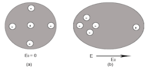
Figure 34: (a) shows thecharge distribution of an atom in absence of electric field while figure (b) show the charge distribution in presence of external electrical field.
Let us consider a single atom of atomic number Z. +e coulomb is the charge of each proton in the nucleus and -e coulomb is the charge of each electron surrounds the nucleus. All electrons in the atom form a spherical cloud of negative charge surrounds the positively charged nucleus. The charge of nucleus is +Ze coulombs and charge of the negative cloud of electrons is -Ze coulombs.
Let us also assume that the negative charge of the electrons cloud is homogeneously distributed on a sphere of radius R. In the absence of external electric field, the center of this sphere and center of nucleus of the atom coincide.
When an external electric field E is applied to the atom. Because of this external electric field the nucleus of the atom is shifted towards negative intensity of the field and the electron cloud is shifted towards the positive intensity of the field.
As due to influence of external electric field the center of nucleus and center of electrons cloud are separated, there will be an attractive force between them according to Coulomb’s law.
Let us suppose x is distance of separation between positive charge nucleus and electron cloud. Also Nucleus is considered as point charge. Hence, the electrostatic force acting on the nucleus =+EZe …….(1) As we know nucleus has been shifted from the center of electrons cloud by a distance x. By using Gauss’s theorem The force is only due to electron cloud acting upon nucleus would only be due to the portion of the cloud enclosed by the sphere of radius x. portion outside the sphere of radius x does not apply any force on the nucleus. Volume of the sphere of radius x = (4/3)πx3 and Volume of the sphere of radius R = (4/3)πR3 Now total negative charge of the electron cloud is -Ze …..(2) Hence, the quantity of negative charge enclosed by the sphere of radius x is, [-Ze/(4/3)πR3] * (4/3)πx3 = -Ze (x3/ R3) ……..(3) According to coulomb’s law = q1q2 /4 πR2 Charge on nucleus q2= Ze So coulomb’s force = {-Ze (x3/ R3) * Ze}/4πƐox2 = Z2e2x/4πƐo R3 ……(4) Note- magnitude is taken into account. Neglect negative sign. i.e. At equilibrium Electrostatic force = Coulomb force . EZe = Z2e2x/4πƐoR3 ……..(5) Upon simplify x = {4πƐoR3/Ze} E Now dipole moment = either charge * separation between charges i.e. x = Ze *{4πƐoR3/Ze} E = 4πƐoR3E Polarization is number of dipole moment per unit volume. Let us suppose N is the number of dipoles per unit volume so Pe=4πƐoR3EN So it is clear that polarization depends upon radius of atom or volume of atom and number of atoms present per unit volume.
|
2. Ionic polarization
Ionic polarization occurred only in that dielectric material in which atoms contain ionic bonds. When such a material is placed in an external electric field the separation between positive charge and negative charge is separated through larger distance as compared to original length.
NaCl and KCl molecule shows ionic polarization occurs. In this polarization the net electric field is zero.
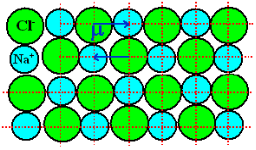
Sodium chloride (NaCl) molecule is formed by ionic bond between sodium and chlorine atoms. Due to electrostatic force between positive sodium and negative chlorine ions, they bound together and form sodium chloride molecule. Because of the presence of inter nucleus distance in the sodium chloride molecule, one might think that an ionic crystal would possess polarization even in the absence external electric filed. Since each pair constitute an electric dipole. But this is not so due to lattice symmetry these dipoles cancel each other’s effect.
|
Figure 35: NaCl crystal
As NaCl have only two atoms or ions there must be a single dipole moment pointing from negative to positive ion in each molecule. But there exists other ionic compounds having more than two atoms.
Number of dipole moments is directly proportional to the number of bonds in a molecule. But all the dipole moments are directed from relatively negative ion to positive ion. The resultant dipole moment of a single molecule would be the vector sum of individual dipole moments of the molecule.
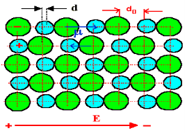
In absence of electric field E, the distance between the ions is d but in presence of electric field, distances between the ions increases.
|
Figure 36: NaCl in the presence of electric field
In the presence of electric field we have certain amount of dipole moment.
|
Figure 37 : Dipole moment.
Hence force F1 due to electric field is F1=qE ……(1) Where q is the net charge on ion. F2 restoring force due to binding force between ions F2=kd …..(2) Where k is spring constant. Here we are considering bond as spring. k may also expressed in terms of other constant which is related to the shape of interatomic potential as young’s modulus or modulus of rigidity as k=Ydo …..(3) At Equilibrium F1 = F2 at equilibrium distance d qE = kd qE = Ydod using (3) d = Now dipole moment p= qd = q2E/Ydo …..(4) and polarization Pi = Nq2E / Ydo ……(5) This is called ionic polarization. This can also be expressed as Pi =NαiE Where αi is constant of proportionality known as ionic polarizability constant. This polarization is independent of temperature.
|
3. Orientational Polarization
Polar dielectric exhibit orientational polarization. In the absence of electric field, the orientation of the molecule are random and hence the net dipole moment is zero when external force is applied the dipole tried to align themselves along the direction of the applied field. This type of polarization is known as orientational polarization.
Ionic polarization: Orientational polarization: This occurs due to the permanent dipole moment in a material. It occurs in elements such as HCl and H2O.
|
Figure 38: Orientational Polarization
Potential energy U of the dipole moment making an angle θ with the electric field. Where p0 is the dipole moment. U=−p0⋅E=−p0Ecosθ According to statistical mechanics, the number of dipoles or molecules making an angle with the electric field is proportional to e−U/kT Letting n(θ) be the number of molecules per unit solid angle at θ, we have n(θ)=n0e+p0Ecosθ/kT
For normal temperatures and fields, the exponent is small, so we can approximate by expanding the exponential:
n(θ)= n0 (1+p0EcosθkT) To find n0 , we integrate over all angles and the result is equal to N. Where N is the total number of molecules per unit volume. The average value of cosθ over all angles is zero, so the integral is just n0 times the total solid angle 4π. We get n0=N4π or N= n0 /4π There exits molecules along the field (cosθ=1) than against the field (cosθ=−1). So in any small volume containing many molecules there will be a net dipole moment per unit volume. As dipole moment is present so polarization Pd is given
Pd =∑unitvolumep0cosθi
Evaluate Total Polarization over solid angle 2πsinθdθ. We have to integrate it
Pd = 0∫π n(θ)p0cosθ2πsinθdθ
Substitute the value of n(θ)
Pd = −N/2 −1∫1 {1+(p0E/kT)cosθ)p0cosθd(cosθ)
By integrating we get,
Pd =Np02E/ 3kT
The polarization is proportional to the field E and depends inversely on the temperature, because at higher temperatures there is more randomness by collisions. This can also be expressed as Pd =αdE Where αd is called dipolar or orientation polarizability and it is equal to p02/ 3kT.
|
4. Space Charge Polarization
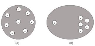
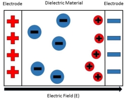
space charge occurs due to accumulation of charge at the electrodes are at the interface in the multiphase material as shown in the figure. the ions diffuse over the appreciable distance in response to the applied field. this gives the rise of redistribution of charges in the dielectric medium
|
Figure 39: Space Charge Polarization
Space charge polarization is also known as Interfacial polarization. Space charge polarization occurs when there is an accumulation of charge at an interface between two materials or between two regions within a material because of an external field.
Space charge polarization can occur when there is a compound dielectric, or when there are two electrodes connected to a dielectric material. This type of electric polarization is different from orientational and ionic polarization because instead of affecting bound positive and negative charges i.e. ionic and covalent bonded structures, interfacial polarization also affects free charges as well.
Interfacial polarization is usually observed in amorphous or polycrystalline solids. Figure 12 shows an example of how free charges can accumulate in a field, causing interfacial polarization.
The electric field will cause a charge imbalance because of the dielectric material's insulating properties. However, the mobile charges in the dielectric will migrate over maintain charge neutrality. This then causes interfacial polarization.
|
Figure 40: This shows how the free positive charges inside the dielectric material migrate towards the negative charge build-up on the right, caused by the external electric field.
The equation to show the space charge polarizability constant is
αc=α - α∞- α0 …………(1)
where αc is the space charge polarizability and α, α∞, and α0 refer to the total, electronic, and orientational polarizations respectively.
It is important to note that because the charges are free charges, defects such as grain boundaries or other interfaces can serve as a medium for interfacial polarizability to form.
From the equation of space charge polarization, it is then determined that the total amount of dielectric polarization in a material is the sum of the electronic, orientational, and interfacial polarizabilities,
or
α=αc+α∞+α0
FREQUENCY DEPENDENCE OF POLARIZATION
- When a dielectric is placed in an electric field the dipoles try to align themselves in the direction of the field. This process requires a finite time that is different for electronic polarization, ionic polarization and dipolar/oreintational polarization.
- As long as the frequency is low i.e. less than 106 hertz polarization is independent of frequency and has same value as in static field.
- As the frequency increases the molecules dipoles will no longer be able to rotate in phase with the frequency of field and hence will begin to lag behind the field.
- As the frequency is still further raised the permanent dipole moment if present in medium will become completely out of phase with the applied field frequency.
- Orientation polarization dies off at high frequencies of the applied field this usually happens in the radio frequency range 106-1011 Hz.
- At still high frequencies usually happens in the radio frequency range 106-1011 Hz, usually happens in the infra-red frequency range 1011-1014 Hz. The positive and negative ions cannot follow the electric field variations, hence contribution from ionic polarization ceases and only electronic polarization remains at high frequencies.
- These effects lead to fall in the permittivity of a dielectric material with increasing frequency and this phenomenon is known as Anomalous Dielectric Dispersion.
Key Takeaways
- When a dielectric material placed in external electrical field , it's molecule gain electric dipole moment and dielectric said to be polarised.
- There are four types of dielectric polarization 1. Electronic polarization 2. Ionic polarization 3. Orientational polarization 4. Space charge polarization
- Electronic polarization refers to the separation of centre of positive charge and centre of negative charge in a material.This separation is caused by high electric field.
- Ionic polarization occurred only in that dielectric material in which atoms contain ionic bonds. When such a material is placed in an external electric field the separation between positive charge and negative charge is separated through larger distance as compared to original length.
- Polar dielectric exhibit orientational polarization. In the absence of electric field, the orientation of the molecule are random and hence the net dipole moment is zero when external force is applied the dipole tried to align themselves along the direction of the applied field. This type of polarization is known as orientational polarization.
- Space charge occurs due to accumulation of charge at the electrodes are at the interface in the multiphase material
This is the most common bridge used for measurement of unknown capacitance, dielectric loss, relative permittivity and power factor. Figure shows the basic circuit arrangement of the bridge and its phasor diagram under balance conditions.
|
Figure 41: (a) Schering bridge for measurement of capacitance (b) Phasor diagram
Two branches consist of non-inductive resistance R3 and a standard capacitor C2. The standard capacitor is usually a high-quality mica capacitor (low-loss) for general measurement or an air capacitor (having very stable value and a very small elastic field) for insulation measurement. One of the arms consists of a variable capacitor connected in parallel with a variable non-inductive resistance R4. The remaining arm consists of unknown capacitor CX whose capacitance is to be determined. Connected in series with a resistance RX to represent loss in the capacitance CX, the impedance of four arms are
we obtain that the dissipation factor is the reciprocal of the quality factor Q and therefore
……………(1) Hence, the dissipation factor tells us about the quality of the capacitor, i.e., how close the phase angle of the capacitor is to the ideal value 90º. Substituting the value of Cx and Rx in Eqn. (1), we have
………….(2)
|
If the frequency and resistor R4 in Schering bridge is fixed, the capacitor C4 can be calibrated to read the dissipation factor directly.
High Voltage Schering Bridge
The Schering bridge is widely used for measurement of small capacitance and dissipation factor, and is then usually supplied from a high voltage or a high frequency source. Figure shows the circuit arrangement for high voltage Schering bridge. The bridge is connected to a high voltage supply through transformer usually at 50 Hz. The vibrational galvanometer is used as a detector.
|
Figure 42: High voltage Schering bridge
The capacitors designed for high voltage are connected in arms ab and ad. The impedance of these two arms is kept very high in comparison to the other two arms bc and cd, so that major portion of the potential drop will be in the arms ab and ad and very small potential drop occurs
in the arms bc and cd. In order to maintain this, the point c is earthed. Hence, for the safety of the operator it is advantageous to locate the controls in arms bc and cd. These controls should be and are at low potential with respect to earth. For the same reason detector is also at low potential.
A spark gap (set to breakdown about 100 V) is connected across arms bc and cd in order to prevent high voltage appearing across arms bc and cd in the case of breakdown of either of the high voltage capacitor.
Earth screens are provided in order to avoid errors caused due to inter-capacitance between high and low impedance arms of the bridge
Key Takeaways
- This is the most common bridge used for measurement of unknown capacitance, dielectric loss, relative permittivity and power factor.
- the dissipation factor is the reciprocal of the quality factor Q and therefore

- The dissipation factor tells us about the quality of the capacitor,
Ferroelectricity, property of certain non-conducting crystals, or dielectrics, that exhibit spontaneous electric polarization (separation of the centre of positive and negative electric charge, making one side of the crystal positive and the opposite side negative) that can be reversed in direction by the application of an appropriate electric field.
A ferroelectric crystal exhibits an electric dipole moment even in the absence of an external electric field. In the ferroelectric state the center of positive charge of the crystal does not coincide with the center of negative charge.
Ferroelectricity is a phenomena discovered in 1921, it is analogous to the ferromagnetic phenomena of iron. Ferroelectric materials do not show any connection with iron at all. The term was devised to explain a spontaneous polarization upon cooling below a curie temperature as well as a display of ferroelectric domains and ferroelectric hysteresis loop. Ferroelectrics (ferroelectric materials) are a subclass of pyroelectric crystals, exhibiting spontaneous polarization; they retain a dipole even after an applied voltage has been removed.
Ferroelectric materials for example, barium titanate (BaTiO3) and Rochelle salt—are composed of crystals in which the structural units are tiny electric dipoles; that is, in each unit the centres of positive charge and of negative charge are slightly separated. In some crystals these electric dipoles spontaneously line up in clusters called domains, and in ferroelectric crystals the domains can be oriented predominantly in one direction by a strong external electric field. Reversing the external field reverses the predominant orientation of the ferroelectric domains, though the switching to a new direction lags somewhat behind the change in the external electric field. This lag of electric polarization behind the applied electric field is ferroelectric hysteresis.
The plot of polarization versus electric field for the ferroelectric states shows a hysteresis loop. A crystal in a normal dielectric state usually does not show significant hysteresis when the electric field is increased and then reversed, both slowly.
Ferroelectricity usually disappears above a certain temperature called the transition temperature. Above the transition the crystal is said to be in a paraelectric state. The term paraelectric suggests an analogy with paramagnetism: there is usually a rapid drop in the dielectric constant as the temperature increases.
In some crystals the ferroelectric dipole moment is not changed by an electric field of the maximum intensity which it is possible to apply before causing electrical breakdown. In these crystals we are often able to observe a change in the spontaneous moment when the temperature is changed. Such crystals are called pyroelectric. Lithium niobate, LiNbO, is pyroelectric at room temperature. It has a high transition temperature and a high saturation polarization.
Some ferroelectric crystals have no Curie point because they melt before leaving the ferroelectric phase.
Examples of Ferroelectric Materials are BaTiO3, PbTiO3, Lead Zirconate Titanate (PZT), Triglycine Sulphate, PVD Lithium tantalite etc.
Barium titanate (BaTiO3 or BTO) was synthesized to become the first and the most widely studied ceramic material, due to its excellent dielectric, ferroelectric and piezoelectric properties .The high dielectric constant of BaTiO3 ceramics results from its crystal structure. BaTiO3 has the perovskite structure as shown in Figure.
Each barium ion is surrounded by 12 oxygen ions. The oxygen ions plus the barium ions form a face-centered cubic lattice. The titanium atoms reside in octahedral interstitial positions surrounded by six oxygen ions. Because of the large size of the Ba ions, the octahedral interstitial position in BaTiO3 is quite large compared to the size of the Ti ions. The Ti ions are too small to be stable in this octahedral position. There are minimum-energy positions off-center in the direction of each of the six oxygen ions surrounding the Ti ion. Since each Ti ion has a +4 charge, the degree of polarization is very high. When an electric field is applied, the Ti ions can shift from random to aligned positions and result in high bulk polarization and high dielectric constant.
|
Figure 43: Barium titanate
Barium titanate has three crystalline forms: cubic, tetragonal, and hexagonal.
Consider the order of magnitude of the ferroelectric effects in barium titanate: the observed saturation polarization P, at room temperature is 8 X l04 esu cm.
The volume of a cell is (4 X 10⁻⁸ )3 = 64 X 10-24 cm3,
So that the dipole moment of a cell is

If the positive ions Ba2+ and Ti4+ were moved by  = 0.1 Å with respect to the negative O-2 ions, the dipole moment of a cell would be 6e
 3 X l0-18 esu-cm. In LiNbO3, the displacements are considerably larger, being 0.9 Å and 0.5 Å for the lithium and niobium ions respectively, giving the larger PS.
APPLICATIONS OF FERROELECTRICS
Ferroelectrics are of theoretical and technical interest because they often have unusually high and unusually temperature-dependent values of the dielectric constant, the piezoelectric effect, the pyroelectric effect, and electro-optical effects, including optical frequency doubling. An advantage of ferroelectric material is its large dielectric constant, which permits the use of physically small capacitors.
The major use of ferroelectrics is in electro-mechanical transducers. This fact arises from the fact that the single crystal increases in dimensions in the direction of spontaneous polarisation. All the dimensions increases equally so that the ceramic appears unpolarised.
The spontaneous polarization of ferroelectric materials implies a hysteresis effect which can be used as a memory function, and ferroelectric capacitors are indeed used to make ferroelectric RAM for computers and RFID cards.
The combined properties of memory, piezoelectricity, and pyroelectricity make ferroelectric capacitors very useful for sensor applications.
Ferroelectric capacitors are used in medical ultrasound machines. The capacitors generate and then listen for the ultrasound ping used to image the internal organs of a body.
Ferroelectric capacitors are used in high quality infrared cameras, fire sensors, sonar, vibration sensors, and even fuel injectors on diesel engines.
Key Takeaways
- A ferroelectric crystal exhibits an electric dipole moment even in the absence of an external electric field.
- In the ferroelectric state the center of positive charge of the crystal does not coincide with the center of negative charge.
- Ferroelectric materials for example, barium titanate (BaTiO3) and Rochelle salt—are composed of crystals in which the structural units are tiny electric dipoles
- The dipole moment of a cell is
|
Reference
- Introduction to Solid State Physics -- Charles Kittel
- Solid State Physics-S 0 Pillai, 8th Ed New Age International Publishers-2018.
- Engineering physics- Gaur and Gupta, & S.Chand Publication
- Engineering physics - Avadhanalu and Kshirsagar, S.Chand Publication


