UNIT – 1
CRYSTALLOGRAPHY AND CRYSTAL DEFECTS
UNIT CELL
BASICS OF CRYSTAL STRUCTURE
Crystallography is the experimental science of determining the arrangement of atoms in the crystalline solids. The properties of some materials are directly related to their crystal structures. So first of we will see what crystal structure is. Crystal structure can be defined as
Crystal structure
A crystal is a solid in which the constituent atoms, molecules or ions are packed in a regularly ordered, repeating pattern extending in three dimensions.
Based on the atomic arrangement in a substance, solids can be broadly classified as either crystalline solids or amorphous solids.
Crystalline Solids
In a crystalline solid, all the atoms are arranged in a periodic manner in all three dimensions. Crystalline solids need extreme temperatures to break the intermolecular forces. They have a definite heat of fusion and melting points because of the uniform arrangement of their components. The local environment is also uniform. However, when cut in any direction, the physical properties are different thus known as anisotropic. When rotated around the axis, the structure of crystals remains the same and that is termed as symmetrical arrangement of molecules, atoms or ions. The refractive index, mechanical strength, thermal conductivity and electrical conductivity of crystalline solids differ in different directions.
Amorphous solids
In a non-crystalline or amorphous solid the atomic arrangement is random or non-periodic in nature. The word amorphous is derived from the Greek word amorphous which means “shapeless”. This is the shapeless, disordered, and irregular arrangement of the constituent particles of a solid. Their inter-molecular forces are not the same nor are the distances between the particles. When cleaved, amorphous solids results in curved surfaces because of their irregular geometric shapes. Thermal conductivity, mechanical strength, electrical conductivity and refractive index are the same in all directions of amorphous solids. This explains where the name isotropic comes from. The solids do not have a sharp melting points or a definite heat of fusion. A wide range of temperature needs to be applied before they can melt because of the absence of an ordered array of components. Examples of amorphous solids include polymers, rubbers, plastics and glass.
Difference between Crystalline solids and amorphous solids
Crystalline solids | Amorphous solids |
|
|
2. They have long range order of regular pattern of arrangement of constituent particles. | 2. They have short range order of regular pattern of arrangement of constituent particles. |
3. They are true solids. | 3. They are pseudo solids or super cooled |
4. They have sharp melting points. | 4. They do not have sharp melting points. |
5. They are anisotropic in nature. | 5. They are isotropic in nature. |
6. They have definite heat of fusion. | 6. They do not have definite heat of fusion. |
Space Lattice or Crystal Lattice
In a solid crystalline material, the atoms or molecules are arranged regularly and periodically in all three dimensions. The atomic arrangement in a crystal is called crystal structure.
To explain crystal symmetries easily, it is convenient to represent an atom or a group of atoms that repeats in three dimensions in the crystal as a unit. If each such atom or unit of atoms in a crystal is replaced by a point in space, then the resultant points in space are called space lattice.
Each point in a space lattice is called a lattice point. Each atom or unit of atoms is called basis or pattern.
A space lattice or crystal lattice is defined as three dimensional infinite arrays of points in space in which every point has surroundings identical to that of every other point in the array.
Basis and Crystal Structure
The atomic arrangement in a crystal is called crystal structure. The crystal structure is formed by associating every lattice point with an atom or an assembly of atoms or molecules or ions, which are identical in composition, arrangement and orientation, called the basis. i.e. an atom, or a group of atoms or molecules identical in composition is called the basis or the pattern.
The basis provides the number of atoms per lattice point, their types, mutual orientations and distances of separation between the atoms.
If the basis is substituted for the lattice points, then the resulting structure is called crystal structure as shown in Figure.
Lattice + basis = crystal structure.
The basis shown in Figure contains two different atoms. In copper and sodium crystals the basis is single atoms; In NaCl, the basis is diatomic and in CaF2 the basis is triatomic. A lattice is an imaginary assumption while the crystal structure is a real concept.
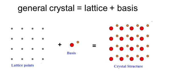
Figure 1: Lattice sites, Basis and crystal structure
Unit Cell and Lattice Parameters
Unit cell is small repeating entity of the atomic structure. It is the basic building block of the crystal structure. It defines the entire crystal structure with the atom positions within.
Unit cells for most of the crystals are parallelepipeds or cubes having three sets of parallel faces. A unit cell is the basic structural unit or building block of the crystal.
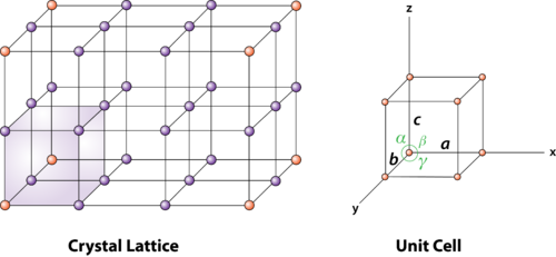
Figure 2 : unit cell and unit cell parameter
A unit cell is defined as the smallest parallelepiped volume in the crystal, which on repetition along the crystallographic axes gives the actual crystal structure or the smallest geometric figure, which on repetition in three-dimensional space, gives the actual crystal structure is called a unit cell.
Choice of a unit cell is not unique but it can be constructed in a number of ways as shown in figure. Following figure shows different ways of representing unit cells in a two-dimensional lattice. A unit cell can be represented as ABCD or A′B′C′D′ or A′′B′′C′′D′′, etc.
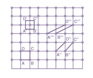
Figure 3: Construction of unit cell in different way
Unit cell parameters or lattice parameters
First we define crystallographic axes. These axes are obtained by the intersection of the three non-coplanar faces of the unit cell. The angles between these faces or crystallographic axes are known as interfacial or interaxial angles. The angles between the axes Y and Z is α, between Z and X is β and between X and Y is γ. The translational vectors or primitives a, b, c of a unit cell along X, Y, Z axes and interaxial angles α, β, γ are called Cell parameters. These cell parameters are shown in (Figure 2). The cell parameters determine the actual size and shape of the unit cell.
Primitive and non-primitive unit cells
The unit cell formed by primitives is called a simple or a primitive unit cell. A primitive unit cell contains only one lattice point. If a unit cell contains more than one lattice point, then it is called a non-primitive unit cell or a multiple unit cell. Most of the unit cells of various crystal lattices contain two or more lattice points and hence it is not necessary that unit cell should be a primitive unit cell.
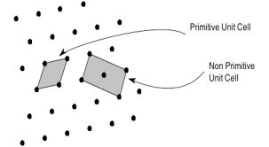
Figure 4: Primitive and non-primitive unit cells
CUBIC SYSTEM
The cubic crystal system is one of the most common (and by far the simplest) class of crystals. As the name itself suggests, all crystal structures of this system have a cube-shaped unit cell with edge length given by the lattice parameter ‘a’.
The three main common representatives are:
- Simple or Primitive Cubic (SC) (also known as primitive cubic)
- Body-centered Cubic (BCC)
- Face-centered Cubic (FCC)

Figure 5: Lattice point locations
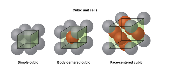
Figure 6: SC, BCC, FCC structure
NUMBER OF ATOMS PER UNIT CELL
Simple or Primitive lattice
In simple or primitive lattice, 8 lattice points or 8 atoms are present at the 8 corners of the unit cell, each contributing 1/8thto the unit cell and hence there will be 8 x 1/8 = 1 lattice point per unit cell.
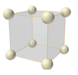
Figure 7: simple or primitive lattice
Body-centered lattice
In body-centered lattice, in addition to the 8 atoms at 8 corners each contributing 1/8thto the unit cell, there will be one complete atom at the center of the unit cell. Therefore number of atoms or lattice points in a body centered unit cell becomes 8 x 1/8 + 1 x 1 = 2.
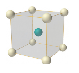
Figure 8: Body-centered lattice
Face-centered lattice (F)
In case of face-centered lattice, in addition to the 8 atoms at 8 corners each contributing 1/8thto the unit cell, six atoms will be present at the center of six faces of the cell each contributing 1/2nd to the unit cell. Therefore number of atoms or lattice points in a face centered unit cell becomes 8 x 1/8 + 6 x 1/2 = 4.
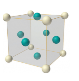
Figure 9: Face-centered lattice (F)
COORDINATION NUMBER
The number of nearest neighbour atoms or ions surrounding an atom or ion is known as coordination number.
It is measure of closeness of packing of atoms in any given structure. It equals the number of nearest neighbour that surrounds each atom.
Simple or Primitive Cubic Crystal
In simple cubic system 6 neighbours atoms at a distance of ‘a’ each from the selected atom as shown in figure. So the coordination number of SC is six.
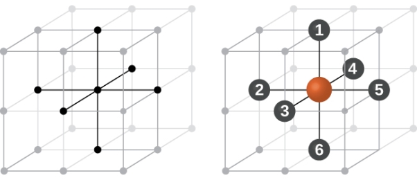
Figure 10: Simple Cubic Crystal
Body Centred Cubic Crystal
In Body Centred Cubic system 8 neighbour atoms are in touch with the selected atom as shown in figure. So the coordination number of BCC is eight.
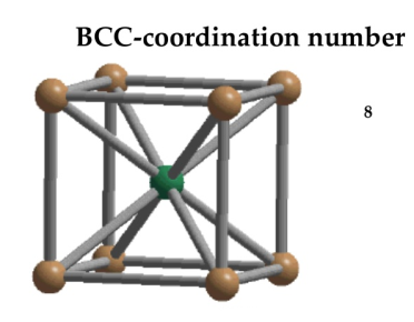
Figure 11: Body Centred Cubic Crystal
Face Centred Cubic Crystal
In Face Centred Cubic system 12 neighbour atoms are in touch with the selected atom as shown in figure. So the coordination number of FCC is twelve.
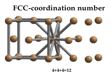
Figure 12: Face Centred Cubic Crystal
ATOMIC RADIUS
Atoms are not hard spheres with distinct boundaries, so their sizes are not determined directly. However, the positions of the atoms in a solid can be determined by x-ray diffraction, and the sizes of the atoms are inferred from those distances.
In this method, the radius of an atom is determined from the unit cell edge length (a), which is determined from the location of the atoms, and the assumption that the atoms touch as shown in below.
Simple or Primitive Cubic Crystal
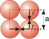
2r = a
Figure 13: Simple or Primitive Cubic Crystal
Body Centred Cubic Crystal
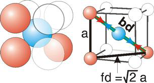
Figure 14: Body Centred Cubic Crystal
Bd | = | 4r |
|
|
|
|
|
|
Bd2 | = | Fd2 + a2 |
|
|
|
|
|
|
(4r)2 | = | 2a2 + a2 = 3a2 |
Face Centred Cubic Crystal
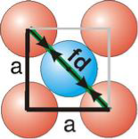
Figure 15: Face Centred Cubic Crystal
Fd | = | 4r |
|
|
|
|
|
|
Fd2 | = | a2 + a2 |
|
|
|
|
|
|
(4r)2 | = | 2a2 |
Relationship of Atomic Radii and Unit Cell Edge Lengths
Setting the edge length equal to 2r in the sc unit cell, and applying the Pythagorean theorem to the triangles shown in Figures we obtain the relationships between the atomic radius (r) of the atom and the edge length of the unit cell (a) given in Equation
For SC r = a/2
For BCC r = 
For FCC r = 
ATOMIC PACKING FACTOR, VOID SPACE, DENSITY OF CRYSTAL
It is impossible to pack spheres without introducing some void space (space that is not occupied). How well the atoms pack a unit cell depends upon the unit cell type and is given by the packing efficiency of the unit cell. Solids with tightly packed unit cells are denser than those with low packing efficiencies. In this section, we examine the packing efficiencies of the cubic unit cells and show how to determine the density of a solid from its crystal structure.
Density
Density is the mass-to-volume ratio of a substance.
Density d = mass of substance / volume of substance
|
Packing Efficiency
Packing efficiency is the fraction of the unit cell that is occupied by particles. Spheres cannot be packed without creating some void space, but the amount of void space depends upon how well they are packed. Packing efficiency (PE) is that fraction of the unit cell volume that is actually occupied by particles, not void space. Thus, the packing efficiency of a unit cell is
Packing Fraction =  |
|
PE =  |
a = the length of a side of the unit cell, so a3 is the volume of the unit cell.
r = the radius of the atoms that occupy the unit cell, so (4/3)πr3 is the volume of a single atom in the unit cell.
N = the number of atoms in the unit cell, so N(4/3)πr3 is the volume occupied by all of the atoms in the unit cell.
The unit cell size (a) is directly proportional to the atom size (r), so one can be defined in terms of the other.
Consequently, the packing efficiency depends only upon the cell type, not its size. As shown in the next sections, the relationship between a and r depends only upon the unit cell type.
Packing in Simple Cubes
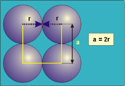
Figure 16: Simple or Primitive Cubic Crystal
In the simple cubic unit cell, the spheres touch along the cell edge. Consequently, the edge length is two atomic radii
(a = 2r).
The properties of the simple cubic unit cell:
r = 0.5a
N = 1 atom/unit cell
PE =  |
Packing efficiency = 52%
Coordination number = 6
Packing in Body-Centered Cubes
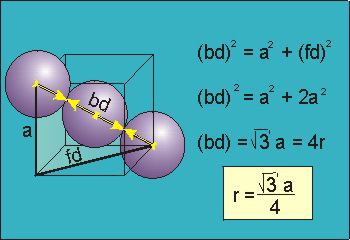
Figure 17: Body Centred Cubic Crystal
For the body-centered cubic unit cell, the spheres make contact along the body diagonal (bd), which is four atomic radii (each yellow arrow is one atomic radius), i.e., bd = 4r.
The body diagonal is related to the face diagonal (fd) and the cell edge (a) by the Pythagorean theorem. The relationship between the cell edge and the face diagonal was derived in the discussion of the fcc unit cell. The properties of the body-centered cubic unit cell:
For BCC r = 
r = 0.433 a
N = 2 atoms/unit cell
PE =  |
Packing efficiency = 68%
Coordination number = 8
Packing in Face-Centered Cubes
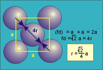
Figure 18: Face Centred Cubic Crystal
For FCC r = 
r= 0.354a
N = 4 atoms/unit cell
PE =  |
Packing efficiency = 74%
Coordination number = 12
As shown in the previous sections, the packing efficiency of a unit cell depends only on the cell type; it is independent of edge length and atomic radius because both cancel in the calculation. As might be expected, the packing efficiency increases as the number of atoms in the unit cell and the number of atoms that are packed around each atom (coordination number) increases.
Table: Packing Efficiencies and Coordination Numbers of Cubic Lattices
Lattice | Packing | Coordination |
Simple | 52% | 6 |
Body-centered | 68% | 8 |
Face-centered | 74% | 12 |
Table for Sc, Bcc, Fcc, Hcp Lattices
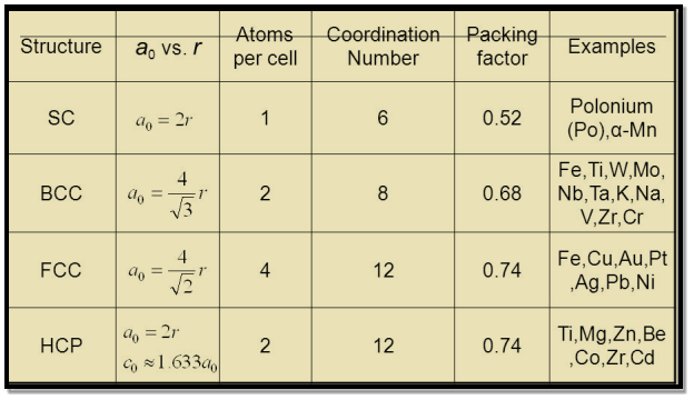
Figure 19: Table for Sc, Bcc, Fcc, Hcp Lattices
DENSITY OF CRYSTAL
The first important thing to understand is that a cubic crystal is made up a crystal lattice or a space lattice structure. And as we have studied before, a space lattice is made up of a repeating arrangement of unit cells. A unit cell is the most basic structure of a crystalline solid.
Hence if we are able to find the density of a unit cell, it can be said that we have found the density of the cubic crystal itself. With this in mind, let us determine how to arrive at the density of a cubic crystal cell.
Now as we know a unit cell also has a cubic structure. It has one, two or four atoms located at various lattice points. Now with the help of geometry, some basic calculations and certain attributes of this cubic structure we can find the density of a unit cell. Let us start with the basic formula for the density of any solid. This formula is
Density = Mass/ Volume
The density of a Unit Cell will be
D = Mass of Unit Cell / Volume of Unit Cell
Mass of a Unit Cell
Now to calculate the mass of one unit cell we add up the mass of all the atoms contained in that particular cell. The number of atoms will depend on the kind of cell it is. So to obtain the mass of a unit cell we multiply the number of atoms “n” into the mass of each atom ”m”.
Mass of Unit Cell = m × n
But now the question remains, what is the mass of an atom? Well, this can be represented in terms of its Avogadro Number (NA)., i.e. number of units in one mole of any substance and the molar mass of an atom. So the mass of an atom can be calculated as
Mass of an Atom = 
Mass of an Atom = 
So now the formula for Mass of Unit Cell is as follows
Mass of Unit Cell = n × 
Volume of Unit Cell
As we already know, the unit cell is a cubic structure. So the Volume of a cube is the cube of the length of the side, Assume that the length of the side of the cube is “a”.
Volume of Unit Cell = a3
Density of Unit Cell
And now we finally arrive at the actual formula for the density of a unit cell
Density of a Unit Cell = 
Density of a Unit Cell = 
Example: An atomic solid crystallizes in a body center cubic lattice and the inner surface of the atoms at the adjacent corner are separated by 60.3 pm. If the atomic weight of A is 48, Find the density of the solid?
Solution:
According to given condition,
0.13 a = 60.3 ⟹ a = 463.8
So Density = 
= 
= 1.75 g/cc
BRAVAIS LATTICE
If the surroundings of each lattice point is same or if the atom or all the atoms at lattice points are identical, then such a lattice is called Bravais lattice.
A space lattice represents the geometrical pattern of crystal in which the surroundings of each lattice point is the same. If the surroundings of each lattice point is same or if the atom or all the atoms at lattice points are identical, then such a lattice is called Bravais lattice.
On the other hand, if the atom or the atoms at lattice points are not same, then it is said to be a non-Bravais lattice.
For representing the type of distribution of lattice points in space, seven different co-ordinate systems are required. These co-ordinate systems are called crystal systems.
The crystal systems are named on the basis of geometrical shape and symmetry. The seven crystal systems are:
(1) Cubic
(2) Tetragonal
(3) Orthorhombic
(4) Monoclinic
(5) Triclinic
(6) Trigonal (or Rhombohedral)
(7) Hexagonal.
In 1948, Bravais showed that 14 lattices are sufficient to describe all crystals. These 14 lattices are known as Bravais lattices and are classified into 7 crystal systems based on cell parameters or lattice points present per unit cell.
Bravais lattices are categorized as
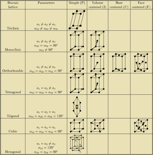
Figure 20: Bravais lattices
Key Takeaways
- A crystal is a solid in which the constituent atoms, molecules or ions are packed in a regularly ordered, repeating pattern extending in three dimensions.
- Based on the atomic arrangement in a substance, solids can be broadly classified as either crystalline solids or amorphous solids.
- Each point in a space lattice is called a lattice point. Each atom or unit of atoms is called basis or pattern.
- A space lattice or crystal lattice is defined as three dimensional infinite arrays of points in space in which every point has surroundings identical to that of every other point in the array.
- Unit cell is small repeating entity of the atomic structure. It is the basic building block of the crystal structure. It defines the entire crystal structure with the atom positions within.
- If the surroundings of each lattice point is same or if the atom or all the atoms at lattice points are identical, then such a lattice is called Bravais lattice.
- The number of nearest neighbour atoms or ions surrounding an atom or ion is known as coordination number.
- Relationship of Atomic Radii and Unit Cell Edge Lengths is given as
For SC r = a/2 , For BCC r =  . For FCC r =
- Packing Fraction =

- Packing efficiency (PE) is that fraction of the unit cell volume that is actually occupied by particles, not void space. Thus, the packing efficiency of a unit cell is
- Density of a Unit Cell =

MILLER INDICES
When dealing with crystalline materials, it often becomes necessary to specify a particular point within a unit cell, a crystallographic direction, or some crystallographic plane of atoms.
Labelling conventions have been established in which three numbers or indices are used to designate point locations, directions, and planes. The basis for determining index values is the unit cell, with a right-handed coordinate system consisting of three (x, y, and z) axes situated at one of the corners and coinciding with the unit cell edges.
For some crystal systems—namely, hexagonal, rhombohedral, monoclinic, and triclinic-the three axes are not mutually perpendicular, as in the familiar Cartesian coordinate scheme. A crystallographic direction is defined as a line between two points, or a vector.
The following steps are utilized in the determination of the three directional indices:
1. A vector of convenient length is positioned such that it passes through the origin of the coordinate system. Any vector may be translated throughout the crystal lattice without alteration, if parallelism is maintained.
2. The length of the vector projection on each of the three axes is determined; these are measured in terms of the unit cell dimensions a, b, and c.
3. These three numbers are multiplied or divided by a common factor to reduce them to the smallest integer values.
4. The three indices, not separated by commas, are enclosed in square brackets, thus: [hkl]. The h, k, and l integers correspond to the reduced projections along the x, y, and z axes, respectively.
Crystal planes are defined as some imaginary planes inside a crystal in which large concentration of atoms are present. Inside the crystal, there exists certain direction along which large concentration of atoms exists. These directions are called crystal directions.
Miller Indices are a method of describing the orientation of a plane or set of planes within a lattice in relation to the unit cell. They were developed by William Hallowes Miller.
Crystal planes and directions can be represented by a set of three small integers called Miller indices [because Miller derived a method of representing crystal planes]. These integers are represented in general as h, k and l. If these integers are enclosed in round brackets as (hkl), then it represents a plane. On the other hand, if they are enclosed in square brackets as [hkl], then it represents crystal direction perpendicular to the above-said plane.
Procedure for drawing the given plane having Miller indices (hkl)
1. A unit cell is drawn with the given lattice parameters. After taking any convenient point as the origin O, the OX, OY and OZ crystallographic axes are to be marked. If lattice parameters are not given, then unit cubic cell of arbitrary lattice constant will be taken.
2. The reciprocals of the Miller indices 1/h, 1/k, 1/l are to be taken. These values provide the intercepts of the given plane on OX, OY and OZ axes, respectively.
3. The intercepts are marked in the unit cell and the plane is drawn.
4. If the intercept is  on any axis, the plane drawn will be parallel to that axis.
Example:
- The (111) surface
Intercepts: a , a , a
Fractional intercepts: 1 , 1 , 1
Miller Indices: (111)
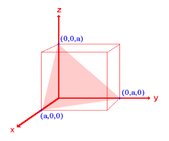 |
Figure 21: The (111) surface
Ii. The (110) surface
Intercepts: a , a , ∞
Fractional intercepts: 1 , 1 , ∞
Miller Indices: (110)
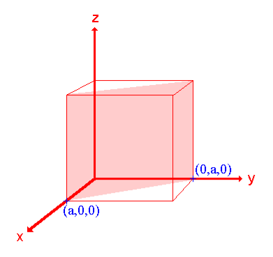 |
|
Figure 22: The (110) surface
Iii. The (210) surface
Intercepts: ½a , a , 
Fractional intercepts: ½ , 1 , 
Miller Indices: (210)
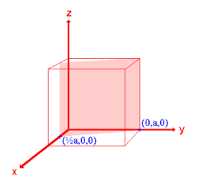 |
|
Figure 23: The (210) surface
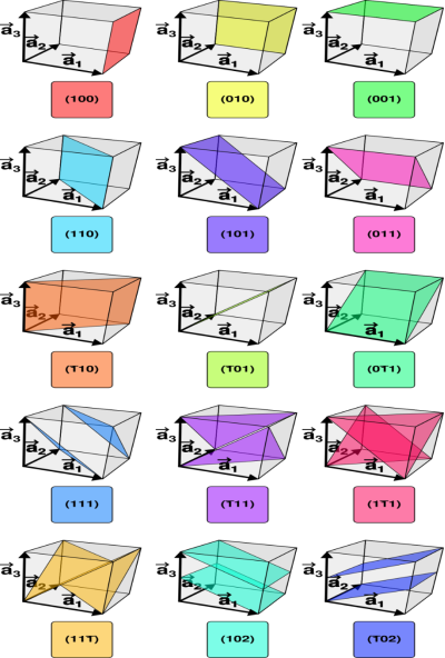
Figure 24: miller planes
INTER PLANNER DISTANCE (BY USING MILLER INDICES)
Distance of separation between successive hkl planes
The separation between successive parallel planes in rectangular axes crystal system can be extracted easily.
Consider a plane ABC which belongs to a family of planes. h, k, l are the Miller indices of this plane, which represents the set of planes. The perpendicular ON from the origin O to the plane represents the inter-planar spacing d = ON of this family of planes. Let ON make an angle α’, β’, γ’ with the x, y, z axes respectively.
The intercepts of the plane on the three axes are OA= a/h; OB= a/k; OC=a/l Where ‘a’ is the length of the cube edge. Then from figure, we have
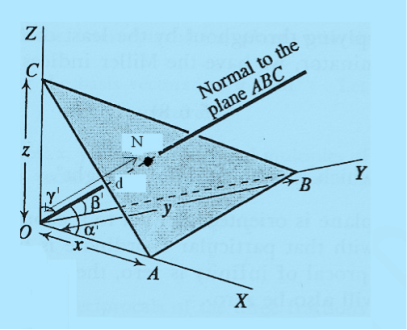
Figure 25: Distance of separation between successive hkl planes
Cos =
=  =
=  =
= 
Cos =
=  =
=  =
= 
Cos =
=  =
=  =
= 
From the figure ON = 
d = 
But, 
Substituting the values of cos’, cos’, cos’ in equation (2), We get,
For the orthogonal coordinates Substituting the values of cos’, cos’, cos’ in equation (2), We get,
(  )2 + (
  )2 +(
)2 +(  )2 = 1
( )2 + (
 )2 +(
)2 +( )2 = 1
( ) (
) ( ) = 1
) = 1
d = 
d = 
Key Takeaways
- Crystal planes are defined as some imaginary planes inside a crystal in which large concentration of atoms are present.
- Inside the crystal, there exists certain direction along which large concentration of atoms exists. These directions are called crystal directions.
- Miller Indices are a method of describing the orientation of a plane or set of planes within a lattice in relation to the unit cell.
- Distance of separation between successive hkl planes is given by d =

BRAGG’S LAW
Consider a set of parallel planes called Bragg’s planes. Each atom is acting as a scattering center. The intensity of the reflected beam at certain angles will be maximum when the path difference between two reflected waves from two adjacent planes is an integral multiple of λ.
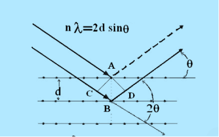
Figure 26: Bragg’s Law
Let ‘d’ be the distance between two adjacent planes, 'λ’ be the wavelength of the incident x-ray, ‘θ’ be the glancing angle.
The path difference between the rays reflected at A & B is given by
 = CB + BD= d sinθ + d sinθ = 2dsinθ
If the two consecutive planes scatter waves in phase with each other, then the path difference must be an integral multiple of wavelength.
 = nλ
= nλ
For the reflected light intensity to be maximum, the path difference
nλ= 2dsinθ
Where ‘n’ is the order of scattering.
This is called Bragg’s law
Therefore, Bragg’s law states that X-rays diffracted from different parallel planes of a crystal interfere constructively when the path difference is integral multiples of wavelength of X-rays.
From Bragg’s law nλ = 2d sin θ, since maximum possible value for sin θ is 1,
nλ/2d ≤ 1 or λ ≤ 2d.
This sets the limitation on the wavelength, i.e. in order to get the diffraction pattern by a crystal, the wavelength of X-rays should not exceed twice the inter-planar spacing.
Importance of Bragg’s law:
1. Bragg’s law is the essential condition to be satisfied by crystal planes in order to get diffraction pattern from a crystal.
2. It is used to calculate inter-planar spacing. Knowing the values of inter-planar spacing, lattice parameters can be determined.
Key Takeaways
- Therefore, Bragg’s law states that X-rays diffracted from different parallel planes of a crystal interfere constructively when the path difference is integral multiples of wavelength of X-rays. It is given as nλ= 2dsinθ
- Bragg’s law is the essential condition to be satisfied by crystal planes in order to get diffraction pattern from a crystal.
Power method is the simplest technique for obtaining x-ray diffraction. It was first used by P.J.W. Debye and P. Scherer. Instead of taking a single crystal having a definite orientation to the x-rays, we can take amass of finely divided crystal with random orientation. In this method, the crystal sample is need not to be taken in large quantity but a little as one milligram of the material is sufficient for study. The power, in fact consists of many small crystals which are oriented in all possible directions. As a result of this x-rays are scattered from all set of planes (e.g., 100,110, etc.). The scattered rays are detected by using an x-ray sensitive film. A narrow beam of x-rays is allowed to fall on the powder. The diffracted x-rays strike a strip of photographic film arranged in the form of circular arc, as shown in the Figure.
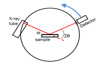
Figure 27: Powder Method
The detector moves in a circle around the sample –The detector position is recorded as the angle 2θ –The detector records the number of X-rays observed at each angle 2θ –The X-ray intensity is usually recorded as “counts” or as “counts per second” . Many powder diffractometers use the Bragg-Brentano parafocusing geometry –To keep the X-ray beam properly focused, the incident angle omega changes in conjunction with 2theta –This can be accomplished by rotating the sample or by rotating the X-ray tube.
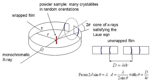
Figure 28 : Power method
In this method no rotation is necessary since the powder sample already contains microcrystal arranged in all possible orientations. Hence, a large number of them will have their lattice planes in correct positions for maximum x-ray reflection to occur. As a result of this we get lighted areas in the form of arcs of lines at different distances from the incident been as shown.
These distances can be converted into scattering angles to be used in the Bragg’s equation for different planes of crystals. Using powder method, the interplanar spacing can be found out since both λ and θ are known. The X-ray powder pattern for sodium chloride is shown in Figure.

Figure 29: X-ray diffraction pattern for sodium chloride
Key Takeaways
- Power method is the simplest technique for obtaining x-ray diffraction.
- In this method, the crystal sample is need not to be taken in large quantity but a little as one milligram of the material is sufficient for study.
- The power, in fact consists of many small crystals which are oriented in all possible directions.
- Using powder method, the interplanar spacing can be found out since both λ and θ are known
A point defect disturbs the crystal pattern at an isolated site. It is useful to distinguish intrinsic defects, which can appear in a pure material, from extrinsic defects, which are caused by solute or impurity atoms. Point defects are lattice defects of zero dimensionality, i.e., they do not possess lattice structure in any dimension. Typical point defects are impurity atoms in a pure metal, vacancies and self-interstitials.
There are three types of point defects: Stoichiometric defect, Schottky defect, Frenkel defect
1. Stoichiometric Defect: In this kind of point defect, the ratio of positive and negative ions (Stoichiometric) and electrical neutrality of a solid is not disturbed. Sometimes it is also known as intrinsic or thermodynamic defects. Fundamentally, they are of two types:
- Vacancy defect: When an atom is not present at their lattice sites, then that lattice site is vacant and it creates a vacancy defect. Due to this, the density of a substance decreases.
- Interstitial defect: It is a defect in which an atom or molecule occupies the intermolecular spaces in crystals. In this defect, the density of the substance increases.
A non-ionic compound mainly shows vacancy and interstitial defects. An ionic compound shows the same in Frenkel and Schottky defect.
2. Schottky Defect
This kind of vacancy defects is found in Ionic Solids. But in ionic compounds, we need to balance the electrical neutrality of the compound so an equal number of anions and cations will be missing from the compound. In this, the size of cations and anions are of almost the same. It reduces the density of the substance.
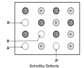
Figure 30: Schottky Defect
3. Frenkel Defect:
In ionic solids generally, the smaller ion (cation) moves out of its place and occupies an intermolecular space. In this case, a vacancy defect is created on its original position and the interstitial defect is experienced at its new position. It is also known as dislocation defect. The density of a substance remains unchanged. It happens when there is a huge difference in the size of anions and cations. Example: ZnS and AgCl
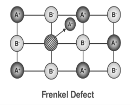
Figure 31: Frenkel Defect
The common point imperfections in crystals are chemical impurities, vacant lattice sites, and extra atoms not in regular lattice positions. Linear imperfections are treated under dislocations; The crystal surface is a planar imperfection, with electron, phonon, and magnon surface states. Some important properties of crystals are controlled as much by imperfections as by the composition of the host crystal, which may act only as a solvent or matrix or vehicle for the imperfections. The conductivity of some semiconductors is due entirely to trace amounts of chemical impurities. The colour and luminescence of many crystals arise from impurities or imperfections. Atomic diffusion may be accelerated enormously by impurities or imperfections. Mechanical and plastic properties are usually controlled by imperfections.
All the defects and impurities described for metals are seen in ionic and molecular compounds as well. Because ionic compounds contain both cations and anions rather than only neutral atoms, however, they exhibit additional types of defects that are not possible in metals.
A point defect occurs when the crystal periodicity is primarily broken at one lattice site or at a few adjacent sites, although its influence can propagate far away into the crystal. The simplest examples of a point defect are substitutions vacancies and interstitials, in which, respectively, atoms on a given site are replaced by a different species, are absent altogether or occupy a position that is usually unoccupied. Substitutional disorder in alloys can be thought as an extreme example of a high density of point defects. Point defects often occurs in pairs up to maintain stoichiometry or charge neutrality, as in the case of Frenkel defects (a vacancy and an interstitial) or Schottky defects (vacancy of ions with opposite charge).
In the case of extended defects, the coordination environment around the defect site is modified to approximate the preferred environment of the new species. For example, if a cation with a preference for tetrahedral coordination is substituted on an octahedral site, the six surrounding anions can be distorted and one or two can be missing altogether, forming an extended defect. If present in sufficient concentration, point defects can give rise to diffuse scattering, in complete analogy to substitutional disorder.
CONCENTRATION OF SCHOTTKY DEFECTS IN METALS AND IONIC CRYSTALS, CONCENTRATION OF FRANKEL DEFECTS
The simplest imperfection is a lattice vacancy, which is a missing atom or ion, also known as a Schottky defect. We create a Schottky defect in a perfect crystal by transferring an atom from a lattice site in the interior to a lattice site on the surface of the crystal. In thermal equilibrium a certain number of lattice vacancies are always present in an otherwise perfect crystal, because the entropy is increased by the presence of disorder in the structure.
In metals with close-packed structures the proportion of lattice sites vacant at temperatures just below the melting point is of the order of to 10-3 to 10-4
But in some alloys, in particular the very hard transition metal carbides such as TiC, the proportion of vacant sites of one component can be as high as 50 percent.
The probability that a given site is vacant is proportional to the Boltzmann factor for thermal equilibrium:
P = exp(-EV/kBT)
Where Ev is the energy required to take an atom from a lattice site inside the crystal to a lattice site on the surface.
If there are N atoms, the equilibrium number n of vacancies is given by the Boltzmann factor
 = exp(-EV/kBT)
If n << N, then
n/N  exp(-EV/kBT)
If E, = 1 eV and T = 1000 K, then n/N  10-5.
10-5.
The equilibrium concentration of vacancies decreases as the temperature decreases. The actual concentration of vacancies will be higher than the equilibrium value if the crystal is grown at an elevated temperature and then cooled suddenly, thereby freezing in the vacancies.
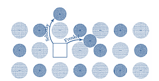
Figure 32: Schottky and Frenkel defects in an ionic crystal. The arrows indicate the displacement of the ions. In a Schottky defect the ion ends up on the surface of the crystal; in a Frenkel defect the ion is removed to an interstitial position.
In ionic crystals it is usually energetically favourable to form roughly equal numbers of positive and negative ion vacancies. The formation of pairs of vacancies keeps the crystal electrostatically neutral on a local scale. From a statistical calculation we obtain
n  Nexp(-Ep/2kBT)
For the number of pairs, where Ep is the energy of formation of a pair.
Another vacancy defect is the Frenkel defect in which an atom is transferred from a lattice site to an interstitial position, a position not normally occupied by an atom. In pure alkali halides the most common lattice vacancies are Schottky defects; in pure silver halides the most common vacancies are Frenkel defects. The calculation of the equilibrium number of Frenkel defects proceeds along the lines of Problem 1. If the number n of Frenkel defects is much smaller than the number of lattice sites N and the number of interstitial sites N', the result is
n  (N N')1/2 exp(-EI/2kBT)
Where EI, is the energy necessary to remove an atom from a lattice site to an interstitial position.
Lattice vacancies are present in alkali halides when these contain additions of divalent elements. If a crystal of KC1 is grown with controlled amounts of CaCl2, the density varies as if a K+ lattice vacancy were formed for each Ca2+ ion in the crystal. The Ca2+ enters the lattice in a normal K+ site and the two C1- ions enter two C1- sites in the KC1 crystal.
Demands of charge neutrality result in a vacant metal ion site. The experimental results show that the addition of CaCl2, to KC1 lowers the density of the crystal. The density would increase if no vacancies were produced, because Ca2+ is a heavier and smaller ion than K+.
The mechanism of electrical conductivity in alkali and silver halide crystals is usually by the motion of ions and not by the motion of electrons. This has been established by comparing the transport of charge with the transport of mass as measured by the material plated out on electrodes in contact with the crystal.
The study of ionic conductivity is an important tool in the investigation of lattice defects. Work on alkali and silver halides containing known additions of divalent metal ions shows that at not too high temperatures the ionic conductivity is directly proportional to the amount of divalent addition.
Key Takeaways
- Point defects are lattice defects of zero dimensionality, i.e., they do not possess lattice structure in any dimension.
- There are three types of point defects: Stoichiometric defect, Schottky defect, Frenkel defect
- Point defects often occurs in pairs up to maintain stoichiometry or charge neutrality, as in the case of Frenkel defects (a vacancy and an interstitial) or Schottky defects (vacancy of ions with opposite charge).
- The probability that a given site is vacant is proportional to the Boltzmann factor for thermal equilibrium:
- P = exp(-EV/kBT)
- For Schottky defects n/N
 exp(-EV/kBT)
 - For Frenkel defects n
 (N N')1/2 exp(-EI/2kBT)
Dislocations are linear defects; they are lines through the crystal along which crystallographic registry is lost. Their principle role in the microstructure is to control the yield strength and subsequent plastic deformation of crystalline solids at ordinary temperatures. Dislocations also participate in the growth of crystals and in the structures of interfaces between crystals. They act as electrical defects in optical materials and semiconductors, in which they are almost always undesirable. Dislocations influence many aspects of physical behaviour, they are studied almost exclusively in Materials Science.
The low observed values of the critical shear stress are explained in terms of the motion through the lattice of a line imperfection known as a dislocation. The concept of dislocations was introduced by Prandtl and Dehlinger.
Dislocations are linear defects that commonly form in metals as a result of the application of stresses due to repeated bending. They play an important role in both the strength and the
Failure of materials: work hardening (such as beating a red-hot piece of metal on an anvil) has been used for centuries by blacksmiths to introduce dislocations into materials, increasing their yield strengths. On the other hand, the infamous metal fatigue fracture are initiated by dislocations, which eventually form persistent slip bands that nucleate short cracks
Two main types of dislocations are identified: edge dislocations and screw dislocation, although most real dislocation are intermediate between these types. They are characterised by two direction vectors: the dislocation direction—the direction of the linear structure in question, and the Burgers vector —the principal direction of the strain (displacement) field near the dislocation.
SCREW DISLOCATION
A screw dislocation marks the boundary between slipped and unslipped parts of the crystal. The boundary parallels the slip direction, instead of lying perpendicular to it as for the edge dislocation. The screw dislocation may be thought of as produced by cutting the crystal partway through with a knife and shearing it parallel to the edge of the cut by one atom spacing.
A screw dislocation transforms successive atom planes into the surface of a helix: this accounts for the name of the dislocation.
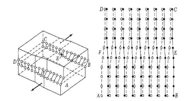
Figure 33: A screw dislocation - A part ABEF of the slip plane has slipped in the direction parallel to the dislocation line EF A screw dislocation may be visualized as a helical arrangement of lattice planes, such that we change planes on going completely around the dislocation line.
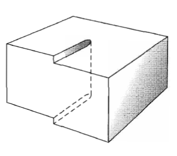
Figure 34: Another view of a screw dislocation. The broken vertical line that marks the dislocation is surrounded by strained material.
EDGE DISLOCATION
Figure shows a simple cubic crystal in which slip of one atom distance has occurred over the left half of the slip plane but not over the right half. The boundary between the slipped and unslipped regions is called the dislocation.
Its position is marked by the termination of an extra vertical half-plane of atoms crowded into the upper half of the crystal as shown in Figure 35. Near the dislocation the crystal is highly strained. The simple edge dislocation extends indefinitely in the slip plane in a direction normal to the slip direction.
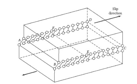
Figure 35: An edge dislocation EF in the glide plane ABCD. The figure shows the slipped region ABEF in which the atoms have been displaced by more than half a lattice constant and the unslipped region FECD with displacement less than half a lattice constant.
The motion of an edge dislocation through a crystal is analogous to the passage of a ruck or wrinkle across a rug: the ruck moves more easily than the whole rug. If atoms on one side of the slip plane are moved with respect to those on the other side, atoms at the slip plane will experience repulsive force from some neighbours and attractive forces from others across the slip plane.
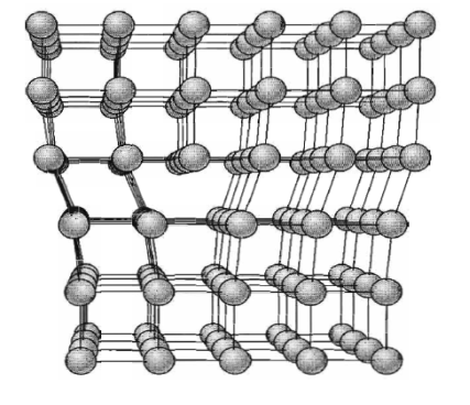
Figure 36: Structure of an edge dislocation. The deformation may be thought of as caused by inserting an extra plane of atoms on the upper half of the axis. Atoms in the upper half-crystal are compressed by the insertion; those in the lower half are extended
These forces cancel to a first approximation. The external stress required to move a dislocation has been calculated and is quite small, below l05 dyn/cm2 when the bonding forces in the crystal are not highly directional. Thus dislocations may make a crystal very plastic. Passage of a dislocation through a crystal is equivalent to a slip displacement of one part of the crystal.
BURGER’S VECTOR
Other dislocation forms may be constructed from segments of edge and screw dislocations. Burgers has shown that the most general form of a linear dislocation pattern in a crystal can be described as shown in Figure.
We consider any closed curve within a crystal, or an open curve terminating oil the surface at both ends:
(a) Make a cut along any simple surface bounded by the line.
(b) Displace the material on one side of this surface by a vector b relative to the other side; here b is called the Burgers vector. (c) In regions where b is not parallel to the cut surface, this relative displacement will either produce a gap or cause the two halves to overlap. In these cases we imagine that we either add material to fill the gap or subtract material to prevent overlap.
(d) Re-join the material on both sides. We leave the strain displacement intact at the time of rewelding, but afterwards we allow the medium to come to internal equilibrium. The resulting strain pattern is that of the dislocation characterized jointly by the boundary curve and the Burgers vector. The Burgers vector must be equal to a lattice vector in order that the rewelding process will maintain the crystallinity of the material.
General method of forming a dislocation ring in a medium. The medium is represented by the rectangular block. The ring is represented by the closed curve in the interior in the block. A cut is made along the surface bounded by the curve and indicated by the contoured area. The material on one side of the cut is displaced relative to that on the other by vector distance b, which may be oriented arbitrarily relative to the surface. Forces will be required to effect the displacement. The medium is filled in or cut away so as to be continuous after the displacement. It is then joined in the displaced state and the applied forces are relaxed. Here b is the Burgers vector of the dislocation.
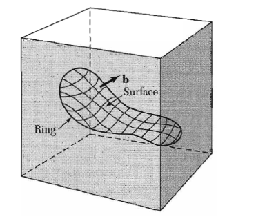
Figure 37 : Burgers vector
The Burgers vector of a screw dislocation (Figures. 33 and 34) is parallel to the dislocation line; that of an edge dislocation (Figures. 35 and 36) is perpendicular to the dislocation line and lies in the slip plane.
Key Takeaways
- Dislocations are linear defects; they are lines through the crystal along which crystallographic registry is lost.
- The low observed values of the critical shear stress are explained in terms of the motion through the lattice of a line imperfection known as a dislocation.
- Dislocations are linear defects that commonly form in metals as a result of the application of stresses due to repeated bending.
- Two main types of dislocations are identified: edge dislocations and screw dislocation, although most real dislocation are intermediate between these types.
- They are characterised by two direction vectors: the dislocation direction—the direction of the linear structure in question, and the Burgers vector —the principal direction of the strain (displacement) field near the dislocation.
Reference
- Introduction to Solid State Physics by Charles Kittel
- Solid State Physics, S.O. Pillai, McGraw Hill Publications
- Engineering Physics, R.K. Gaur and S.L. Gupta, Dhanapat Rai Publications
- A Text Book of Engineering Physics, M.N. Avadhanulu, P.G. Kshirsagar, S. Chand and Company Ltd.