Unit - 1
Diodes and Applications
Basically, a diode is a two terminal device that allows current to flow in one direction when a voltage is applied across the terminals.
Diodes have polarity, determined by an anode (positive lead) and cathode (negative lead).
When a diode allows current flow, it is forward-biased. When a diode is reverse-biased, it acts as an insulator and does not permit current to flow.
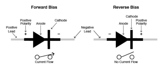
The symbol of a diode is shown in figure. The arrowhead points in the direction of conventional current flow in the forward biased condition. That means the anode is connected to the p side and the cathode is connected to the n side.
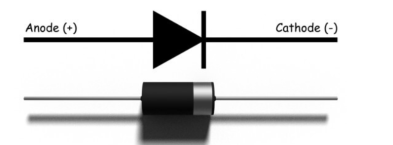
A diode’s working principle depends on the interaction of n-type and p-type semiconductors. An n-type semiconductor has plenty of free electrons and a very few numbers of holes. A p-type semiconductor has a high concentration of holes and a low concentration of free electrons.
Unbiased Diode
When one n-type region and one p-type region come in contact because of concentration differences, majority carriers diffuse from one side to another. As the concentration of holes is high in the p-type region and it is low in the n-type region, the holes start diffusing from the p-type region to the n-type region.
Again, the concentration of free electrons is high in the n-type region and it is low in the p-type region the free electrons start diffusing from the n-type region to the p-type region.
The free electrons diffusing into the p-type region from the n-type region recombine with holes available there and create uncovered negative ions in the p-type region. In the same way, the holes diffusing into the n-type region from the p-type region would recombine with free electrons available there and create uncovered positive ions in the n-type region.
In this way, a layer of negative ions in the p-type side and a layer of positive ions in the n-type region appear along the junction line of these two types of semiconductors. The layers of uncovered positive ions and uncovered negative ions form a region in the middle of the diode where no charge carrier exists since all the charge carriers get recombined here in this region. Due to the lack of charge carriers, this region is called the depletion region.
After the formation of the depletion region no diffusion of charge carriers from one side to another in the diode. This is due to the electric field appeared across the depletion region which prevent further migration of charge carriers from one side to another.
The potential of the layer of uncovered positive ions in the n-type side would repel the holes in the p-type side and the potential of the layer of uncovered negative ions in the p-type side would repeal the free electrons in the n-type side. That means a potential barrier is created across the junction to prevent further diffusion of charge carriers.

Forward Biased Diode
If a positive terminal of a source is connected to the p-type side and the negative terminal of the source is connected to the n-type side of the diode and if we increase the voltage of this source slowly from zero.
Initially, there is no current flowing through the diode the majority charge carriers do not get sufficient influence of the external field to cross the depletion region. Because the depletion region acts as a potential barrier against the majority charge carriers.
This potential barrier is called forward potential barrier. The majority charge carriers start crossing the forward potential barrier only when the value of externally applied voltage across the junction is more than the potential of the forward barrier. For silicon diodes, the forward barrier potential is 0.7 volt and for germanium diodes, it is 0.3 volt.
When the externally applied forward voltage across the diode becomes more than the forward barrier potential, the free majority charge carriers start crossing the barrier and contribute the forward diode current. At this stage the diode behaves as a short-circuited path, and forward current gets limited by only externally connected resistors to the diode.
Reverse Biased Diode
If we connect the negative terminal of the voltage source to the p-type side and positive terminal of the voltage source to the n-type side of the diode. At that condition, due to electrostatic attraction of the negative potential of the source, the holes in the p-type region would be shifted more away from the junction leaving more uncovered negative ions at the junction.
In the same way, the free electrons in the n-type region would be shifted more away from the junction towards the positive terminal of the voltage source leaving more uncovered positive ions in the junction.
As a result, the depletion region becomes wider. This condition of a diode is called the reverse biased condition. At this condition, no majority carriers cross the junction, and they instead move away from the junction. In this way, a diode blocks the flow of current when it is reverse biased.
As a result, there is a tiny current flowing through the diode from positive to the negative side. The amplitude of this current is too small as the number of minority charge carriers in the diode is too small. This current is called reverse saturation current.
Application
Diode as a Rectifier
The most common and important application of a diode is the rectification of AC power to DC power. The basic types of these rectifier circuits are half wave, full wave centre tapped and full bridge rectifiers. A single or combination of four diodes is used in most of the power conversion applications. The figure shows diode operation in a rectifier.

Diode as a Rectifier
Diodes in Clipping Circuits
Clipping circuits are used in FM transmitters where noise peaks are limited to a particular value so that excessive peaks are removed from them. The clipper circuit is used to put off the voltage beyond the pre-set value without disturbing the remaining part of the input waveform.

Diodes in Clamping Circuits
A clamper circuit is used to shift or alter either positive or negative peak of an input signal to a desired level. This circuit is also called as level shifter or DC restorer.
 Clamping Circuit
Diodes in Logic Gates
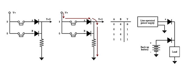
Diodes can also perform digital logic operations. Low and high impedance states of logic switch are analogous to the forward and reverse-biased conditions of the diode respectively. Thus, the diode can perform logic operations such as AND, OR, etc. The below figure shows the OR gate logic implemented using a pair of diodes and a resistor.
Diodes in Logic Gates
In the above circuit input voltage is applied at V and by controlling the switches we get the OR logic at the output. Here logic 1 means high voltage and logic 0 means zero voltage. When both switches are in open state, both the diodes are in reverse-biased condition and hence the voltage at the output Y is zero. When any one of the switches is closed, the diode becomes forward-bias and as a result the output is high.
Diodes in Voltage Multiplier Circuits
Voltage multiplier consist of two or more diode rectifier circuits which are cascaded to produce a DC output voltage equal to the multiplier of the applied input voltage. These multiplier circuits are of different types like voltage doubler, tripler, quadrupler, etc. By the usage of diodes combination with capacitors, we get the odd or even multiple of the input peak voltage at the output.
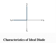
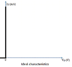
In an ideal diode, there would be no voltage drop across it when forward biased. All the source voltages would be dropped across circuit resistors and there is no voltage drop across the diode.
In an ideal diode, when reversed bias, it would have infinite resistance, causing zero current flow.

Practical Diodes
A practical diode does offer some resistance to current flow when forward bias. Since there is some resistance there will be some power dissipated when current flows through a forward bias diode.
Therefore, there is a practical limit to the amount of current a diode can conduct without damage. A reverse bias diode has very high resistance. Excessive reverse bias can cause the diode to conduct.

Resistance is the opposition offered to the flow of current. The diode resistance can be defined as the effective opposition offered by the diode to the flow of current. When the diode is forward biased it offers zero resistance and infinite resistance when reverse biased.
Forward Resistance:
In forward the diode will not conduct till it reaches the minimum threshold voltage level. After the applied voltage exceeds the threshold level the diode starts conducting. The resistance in this condition is called forward resistance of the diode. Hence forward resistance is the resistance offered by the diode when diode works in forward biased condition.
Forward resistance is classified as static and dynamic depending on the current flowing through the device that is DC or AC.
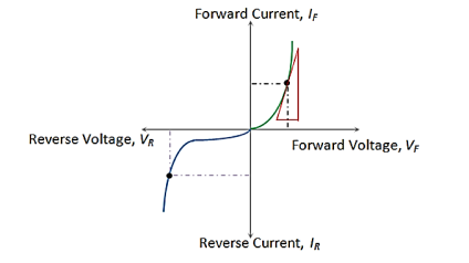
Static or DC Resistance
It is the resistance offered by the diode to the flow of DC through it when we apply a DC voltage to it. The static resistance is expressed as the ratio of DC voltage applied across the diode terminals to the DC flowing through it shown by dotted lines in the figure
Rdc = Vdc/Idc
Dynamic or AC Resistance
It is the resistance offered by the diode to the flow of AC through it when the circuit is connected which has AC voltage which is an active circuit element. The dynamic resistance is given as the ratio of change in voltage applied across the diode to the resulting change in the current flowing through it.
This is shown by the slope-indicating red solid lines which is given by
Rac=vac/iac
In Diode Equivalent Models the Shockley’s equation gives the exponential relationship between current and voltage, but every time while using diodes in a circuit, there is no need to apply exponential formula to find the values of voltage or current.
Therefore, we can approximate the characteristic of diode by replacing the diode in the circuit with its equivalent circuit. An equivalent circuit is nothing but a combination of elements that represents the actual terminal characteristics of the device.
In simple language, it simply means the diode in the circuit can be replaced by other elements without severely affecting the behaviour of circuit.
The diode can be modelled in three different ways depending on the accuracy required.
The three models are:
1. Ideal Diode Model
2. Simplified Model
3. Piece-Wise Linear Model
Ideal Diode Model:
This indicates that the voltage drop across the diode is zero for any value of diode current. The ideal diode does not allow any current to flow in reverse biased condition. The current flowing through the diode is zero for any value of reverse biased voltage. The ideal diode can be modelled as open or closed switch depending on the bias voltage. Hence, the ideal diode can be modelled as closed switch under forward biased condition. This is shown in figure
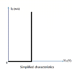
Simplified Model
The equivalent model in this case consists of a battery and an ideal diode. Consider the horizontal line from (0 to 0.7 V) in the curve. The horizontal line indicates that the current flowing through diode is zero for voltages between 0 and 0.7 V.
To model the behaviour, we put a battery of 0.7 V in the equivalent diode model. When you measure the voltage across an isolated diode, the instrument will show zero value. The battery simply indicates that it opposes the flow of current in forward direction until 0.7 V. As the voltage becomes larger than 0.7 V, the current starts flowing in forward direction.
Piece-Wise Linear Model
The piece-wise linear model is a model in which the characteristics of diode is approximated by “piece-wise linear” line segments. Now consider the straight line in the piece-wise linear characteristics. This straight line indicates constant slope. Slope in the V-I graph indicates resistance. So, we add a resistor in the diode model. The value of resistance can be found from the graph.
We can see from the graph that the diode current changes from 0 to 15 mA for a voltage change from 0.7 to 0.8 V. Thus, the average value of resistance is (0.8 V-0.7 V)/ (15 mA - 0 mA) = 6.67 Ω.
Thus, the value of resistance in the equivalent model is approximately 6.67 Ω. The figure given below shows piece-wise linear characteristics of diode along with the It’s model.
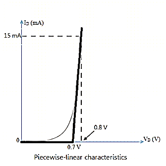
In the graph shown on left, the actual characteristics of diode is superimposed by piece-wise linear characteristics. The piece-wise linear characteristics does not exactly represent the characteristics of diode. However, it provides a good first approximation to the actual characteristics of the diode. Piecewise linear characteristics can be obtained by replacing the diode in the circuit with a resistor, a battery, and an ideal diode. This is shown in the right side of the above figure.

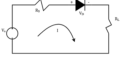
-Vs + I Rs + Vd + I RL =0
I = Vs -Vd / Rs + RL
A plot of the current, I, versus the voltage drop across the diode, VD, will yield a straight line, called the "Load Line", of possible values of current flow in the circuit. The line is formed with I = 0 at VD = VS and that
I = VD/ (RS + RL) at VS = 0, as shown below:
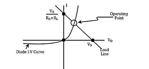
The "Operating Point" is found through the second equation that relates I and VD, namely the diode equation
I = I0[exp (VD/KBT) - 1].
The I-V relation for the diode will cross the Load Line at the Operation Point represented by open circle. This provides a graphical solution for the currents and voltages in a circuit with a diode.
When the source voltage changes with time that is VS = VS(t), The Load Line varies with time that is the slope is constant at dI/dV = -1/ (RS + RL) while the intercept shifts, as shown below.
When VS(t) varies symmetrically around zero, as with the AC line, we see that the maximum positive value of VS(t) leads to the maximum current flow, while the maximum negative value of VS(t) leads to a minimal current, so that asymptotically I (VS → -∞) → -I0.

The rhythmic change in Operating Point (open circles is the basis of the half-wave rectifier
When the specified voltage is exceeds the diode resistance gets increased, making the diode reverse biased and acts as an open switch. Whenever the voltage applied is below the reference voltage, the diode resistance gets decreased, making the diode forward biased, and it acts as a closed switch.
The following circuit explains the diode acting as a switch.
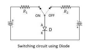
A switching diode has a PN junction in which P-region is lightly doped and N-region is heavily doped. The above circuit symbolizes that the diode gets ON when positive voltage forward biases the diode and it gets OFF when negative voltage reverse biases the diode.
The half-wave rectifier circuit consists of three main parts:
- A transformer
- A resistive load
- A diode
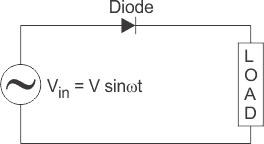
The half wave rectifier is shown in the diagram
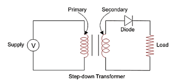
Initially a high AC voltage is applied to the to the primary side of the step-down transformer and a low voltage is obtained at the secondary winding which is applied to the diode.

During the positive half cycle of the AC voltage, the diode will be forward biased and the current flows through the diode. During the negative half cycle of the AC voltage, the diode will be reverse biased, and the flow of current will be blocked. The final output voltage waveform on the secondary side (DC) is shown in figure above.
At the secondary side of the circuit, if we replace the secondary transformer coils with a source voltage, we can simplify the circuit diagram of the half-wave rectifier as:
For the positive half cycle of the AC source voltage, the equivalent circuit effectively becomes:
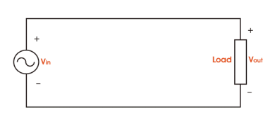
This is because the diode is forward biased and allows current to pass through. Therefore, we have a closed circuit.
For the negative half cycle of the AC source voltage, the equivalent circuit becomes:

Because the diode is now in reverse bias mode, no current will pass through it. Because it is no current can flow through to the load during this time and the output voltage is equal to zero.
Here is what the half wave rectifier waveform looks like on the input side (Vin), and what it looks like on the output side (Vout) after rectification that is conversion from AC to DC.

The graph above actually shows a positive half wave rectifier. This is a half-wave rectifier which only allows the positive half-cycles through the diode, and blocks the negative half-cycle.
Conversely, a negative half-wave rectifier allows negative half-cycles through the diode and will block the positive half-cycle. The only difference between a positive and negative half wave rectifier is the direction of the diode.
Half Wave Rectifier with Capacitor Filter
Filters are components used to convert or smoothen pulsating DC waveforms into constant DC waveforms. This is achieved suppressing the DC ripples in the waveform.
Although half-wave rectifiers without filters are theoretically possible, they cannot be used for any practical applications. As DC equipment requires a constant waveform, we need to ‘smooth out’ this pulsating waveform hence half wave rectifier is used with filter. A capacitor or an inductor can be used as a filter – but half wave rectifier with capacitor filter is mostly used.
The circuit diagram below shows how a capacitive filter is can be used to smoothen out a pulsating DC waveform into a constant DC waveform.
 Ripple Factor of Half Wave Rectifier
‘Ripple’ is the unwanted AC component remaining when converting the AC voltage waveform into a DC waveform. Even though we try to remove all AC components, there lies some small amount left on the output side which pulsates the DC waveform. This undesirable AC component is called ‘ripple’.
The ripple factor is the ratio between the RMS value of the AC voltage (on the input side) and the DC voltage (on the output side) of the rectifier.
The formula for ripple factor is:

Which can also be rearranged to equal:
Ripple factor (γ) = (I 2 rms – I 2 dc) / Idc = 1.21
The ripple factor of half wave rectifier is equal to 1.21 (i.e., γ = 1.21).
Efficiency of Half Wave Rectifier
Rectifier efficiency (η) is the ratio between the output DC power and the input AC power. The formula for the efficiency is equal to:
ղ = Pdc / Pac
The efficiency of a half wave rectifier is equal to 40.6% (i.e., ηmax = 40.6%)
RMS value of Half Wave Rectifier
To derive the RMS value of half wave rectifier, we need to calculate the current across the load.
If the instantaneous load current is equal to iL = Imsinωt, then the average of load current (IDC) is equal to:
Idc = 1/ 2 π  sinwt = Im / π
Where Im is equal to the peak instantaneous current across the load (Imax). Hence the output DC current (IDC) obtained across the load is:
Idc = Imax /π where I max = maximum amplitude of dc current
For a half-wave rectifier, the RMS load current (Irms) is equal to the average current (IDC) multiple by π/2. Hence the RMS value of the load current (Irms) for a half wave rectifier is:
I rms = Im /2
Where Im= Imax which is equal to the peak instantaneous current across the load.
Peak Inverse Voltage of Half Wave Rectifier
Peak Inverse Voltage (PIV) is the maximum voltage that the diode can withstand during reverse bias condition. If a voltage is applied more than the PIV, the diode will be destroyed.
Form Factor of Half Wave Rectifier
Form factor (F.F) is the ratio between RMS value and average value, as shown in the formula below:
F.F = RMS value / Average value
The form factor of a half wave rectifier is equal to 1.57 (i.e., F. F= 1.57).
Output DC Voltage
The output voltage (VDC) across the load resistor is denoted by:
VDC = Vs max / π where Vs max = maximum amplitude of secondary voltage.
Applications of Half Wave Rectifier
- For rectification applications
- For signal demodulation applications
- For signal peak applications
Full wave rectifier:
The circuits which convert alternating current (AC) into direct current (DC) are known as rectifiers. If such rectifiers rectify both the positive and negative half cycles of an input alternating waveform, the rectifiers are referred as full wave rectifiers.
A centre-tapped full wave rectifier system consists of:
- Centre-tapped Transformer
- Two Diodes
- Resistive Load
Centre-tapped Transformer: – It is a normal transformer with one slight modification. It has an addition wire connected to the exact centre of the secondary winding. This type of construction divides the AC voltage into two equal and opposite voltages namely +Ve voltage (Va) and -Ve voltage (Vb).
The total output voltage is
V = Va + Vb
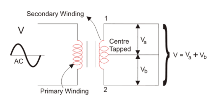
The circuit diagram is as follows
Working of Centre-tapped Full Wave Rectifier
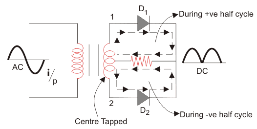
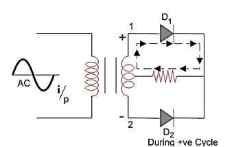
We apply an AC voltage to the input transformer. During the positive half-cycle of the AC voltage, terminal 1 will be positive, centre-tap will be at zero potential and terminal 2 will be negative potential. This will lead to forward bias in diode D1 and cause current to flow through it.
During this time, diode D2 is in reverse bias and will block current through it.
During the negative half-cycle of the input AC voltage, terminal 2 will become positive with relative to terminal 2 and centre-tap. This will lead to forward bias in diode D2 and cause current to flow through it. During this time, diode D1 is in reverse bias and will block current through it.
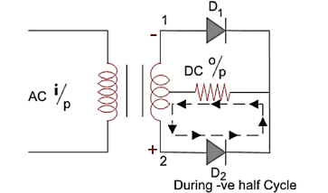
During the positive cycle, diode D1 conducts and during negative cycle diode D2 conducts and during positive cycle. As a result, both half-cycles are allowed to pass through. The average output DC voltage here is almost twice of the DC output voltage of a half wave rectifier.

Filter Circuit
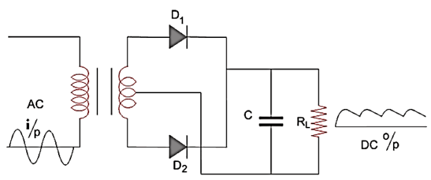
We get a pulsating DC voltage with a lot of ripples as the output of the centre-tapped full wave rectifier.
For practical applications we cannot use this pulsating signal. So, to convert the pulsating DC voltage to pure DC voltage, we use a filter circuit as shown above. Here the capacitor is placed across the load.
The working of the capacitive filter circuit is to short the ripples and block the DC component so that it flows through another path and is available across the load. During the positive half-wave, the diode D1 starts conducting. The capacitor is uncharged, and when we apply an input AC voltage which happens to be more than the capacitor voltage, it charges the capacitor immediately to the maximum value of the input voltage. At this point, the supply voltage is equal to capacitor voltage.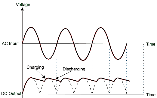
When the applied AC voltage starts decreasing and less than the capacitor, the capacitor starts decreasing slowly which is slower when compared to the charging of the capacitor and it does not get enough time to discharge entirely and the charging starts again.
So around half of the charge present in the capacitor gets discharged. During the negative cycle, D2 starts conducting, and the above process repeats. This will cause the current to flow through the same direction across the load.
Characteristics:
Ripple Factor (γ)
γ=
The output of the rectifier consists of both AC and DC components. The AC components are undesirable to us and will cause pulsations in the output. This unwanted AC components are called Ripple. The expression ripple factor is given above where Vrms is the RMS value of the AC component and Vdc is the DC component in the rectifier.
For centre-tapped full-wave rectifier, we obtain γ = 0.48
Rectifier Efficiency (η)
Rectifier efficiency is the ratio between the output DC power and the input AC power.
ղ = Pdc / Pac
For centre-tapped full-wave rectifier, ηmax = 81.2%
Form Factor (F.F)
The form factor is the ratio between RMS value and average value.
FF = RMS value / Average value
For centre-tapped full wave rectifier, FF = 1.11
Advantages of Full Wave Rectifiers
- Full wave rectifiers have higher rectifying efficiency than half wave rectifiers. This means that they convert AC to DC more efficiently.
- They have low power loss because no voltage signal is wasted in the rectification process.
- The output voltage of centre-tapped full wave rectifier has lower ripples than a halfwave rectifiers.
Disadvantages of Full Wave Rectifiers
- The centre-tapped rectifier is more expensive than half-wave rectifier and tends to occupy a lot of space.
The following two processes cause junction breakdown due to the increase in reverse bias voltage.
(i) Zener Breakdown
(ii) Avalanche Breakdown
Zener Breakdown
The Zener Breakdown is observed in the Zener diodes having Vz less than 5V or between 5 to 8 volts. When reverse voltage is applied to a Zener diode, it causes high intense electric field to appear across a narrow depletion region. Such an intense electric field is strong enough to pull some of the valence electrons into the conduction band by breaking their covalent bonds and these electrons become free electrons available for conduction.
Many such free electrons constitute a large reverse current through the Zener diode and breakdown is said to have occurred due to the Zener effect.
Characteristics of Zener Breakdown is shown below:
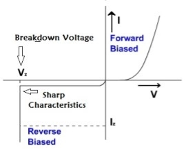
Zener Breakdown Characteristics
A current limiting resistance should be connected in series with the Zener diode to protect it against the damage due to excessive heating. In Zener breakdown, the breakdown voltage depends on the temperature of P-N junction. The breakdown voltage decreases with increase in the junction temperature.
Avalanche Breakdown
The avalanche breakdown is observed in the Zener Diodes having Vz having greater than 8 V. In the reverse biased condition, the conduction will take place only due to the minority carriers. As we increase the reverse voltage applied to the Zener diode, these minority carriers tend to get accelerated. Therefore, the kinetic energy associated with them increases. While travelling, these accelerated minority carriers will collide with the stationary atoms and impart some of the kinetic energy to the valence electrons present in the covalent bonds.
Characteristics of Avalanche Breakdown is shown below:
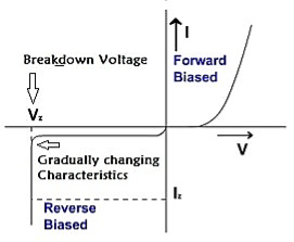
Avalanche Breakdown Characteristics
Due to this additionally acquired energy, these valence electrons will break their covalent bonds and jump into the conduction bond to become free conduction. The newly generated free electrons get accelerated. They will knock out some more valence electrons by means of collision. This phenomenon is called as carrier multiplication.
Zener Diode
- Zener diode is a special type of p-n junction semiconductor diode in this diode the reverse breakdown voltage is adjusted precisely between 3v to 200v.
- Its applications are based on this principle hence Zener diode is called as a breakdown diode.
- The doping level of the imparity added to manufacture the Zener diode is controlled to adjust the precise value of breakdown voltage.
PRINCIPLE OF OPERATION: - A Zener diode can be forward biased or reverses biased. Its operation in the forward biased mode is same as that of a p-n junction diode but its operation in the reverse biased mode is sustainably different.

When in reverse mode as usual in most of its applications, a small leakage current may flow. As the reverse voltage increases to the predetermined breakdown voltage (Vz), current starts flowing through the diode.
The current increases to maximum, which is determined by the series resistor which stabilizes and remains constant over a wide range of applied voltage.
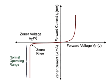
The above diagram shows the V-I characteristics of a zener diode. When the diode is connected in forward bias, this diode acts as a normal diode but when the reverse bias voltage is greater than zener voltage, a sharp breakdown takes place. In the V-I characteristics above Vz is the zener voltage. It is also the knee voltage because at this point the current increases rapidly.
Zener diodes are used for voltage regulation, as reference elements, surge suppressors, and in switching applications and clipper circuits.
Numerical:
A 5.0V stabilized power supply is required to be produced from a 12V DC power supply input source. The maximum power rating PZ of the zener diode is 2W. Using the zener regulator circuit above calculate:
a). The maximum current flowing through the zener diode.
Maximum current = Watts/ Voltage =2W/5V =400mA
b). The minimum value of the series resistor, RS
 = 17.5 Ω
c). The load current IL if a load resistor of 1kΩ is connected across the zener diode.

d). The zener current IZ at full load.
Iz =Is -Il =440mA – 5mA = 395mA
Optoelectronics is the study and application of electronic devices that use light. Such devices include those that emit light (LEDs and light bulbs), channel light (fibre optic cables), detect light (photodiodes and photoresistors), or are controlled by light (opto-isolators and phototransistors).
LEDs (Light Emitting Diodes) are semiconductor light sources that combine a P-type semiconductor (larger hole concentration) with an N-type semiconductor (larger electron concentration).
Applying a sufficient forward voltage will cause the electrons and holes to recombine at the P-N junction, releasing energy in the form of light.
In comparison with conventional light sources that first convert electrical energy into heat, and then into light, LEDs (Light Emitting Diodes) convert electrical energy directly into light, delivering efficient light generation with little-wasted electricity.

Definition: A special type of PN junction device that generates current when exposed to light is known as Photodiode. It is also known as photodetector or photosensor. It operates in reverse biased mode and converts light energy into electrical energy. It works on the principle of Photoelectric effect.
The figure below shows the symbolic representation of a photodiode:
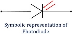
Construction of Photodiode
The figure below shows the constructional detail of a photodiode:
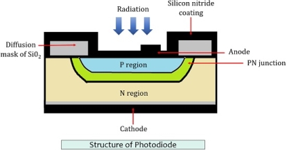
The PN junction of the device placed inside a glass material to allow the light energy to pass through it. Because the junction is exposed to radiation, thus, the other portion of the glass material is painted black or is metallised.
Operational Modes of Photodiode
Photodiode basically operates in two modes:
Photovoltaic mode: It is also known as zero-bias mode because no external reverse potential is provided to the device. However, the flow of minority carrier will take place when the device is exposed to light.
Photoconductive mode: When a certain reverse potential is applied to the device then it behaves as a photoconductive device. Here, an increase in depletion width is seen with the corresponding change in reverse voltage.
Working of Photodiode
In the photodiode small reverse current flows through the device termed as dark current. It is called so because this current is the result of the flow of minority carriers and flows when the device is not exposed to radiation.
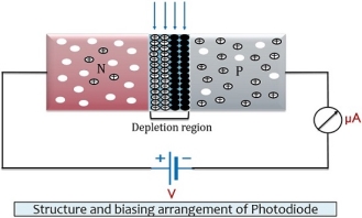
The electrons present in the p side and holes present in n side are the minority carriers. When a certain reverse-biased voltage is applied holes being the minority carrier that is holes from n-side experiences repulsive force from the positive potential of the battery.
Similarly, the electrons present in the p side experience repulsion from the negative potential of the battery. Due to this movement electron and hole recombine at the junction resultantly generating depletion region at the junction.
Due to this movement, a small reverse current flow through the device known as dark current.
When the junction of the device is illuminated with light. As the light falls on the surface of the junction, then the temperature of the junction gets increased. This causes the electron and hole to get separated from each other.
At the two gets separated then electrons from n side gets attracted towards the positive potential of the battery. Similarly, holes present in the p side get attracted to the negative potential of the battery.
This movement then generates high reverse current through the device.
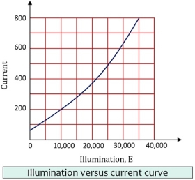
With the rise in the light intensity, more charge carriers are generated and flow through the device. Thereby, producing a large electric current through the device.
Hence the intensity of light energy is directly proportional to the current through the device. Only positive biased potential can put the device in no current condition in case of the photodiode.
CHARACTERISTICS OF PHOTODIODE
The figure below shows the VI characteristic curve of a photodiode:
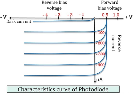
Here, the vertical line represents the reverse current flowing through the device and the horizontal line represents the reverse-biased potential.
The first curve represents the dark current that generates due to minority carriers in the absence of light. The current proportionally increases with the luminous flux hence there is equal spacing.
The figure below shows the curve for current versus illumination:
Applications of Photodiode
- Photodiodes majorly find its use in counters and switching circuits.
- Photodiodes are extensively used in an optical communication system.
- Logic circuits and encoders also make use of photodiode.
- It is widely used in burglar alarm systems. In such alarm systems, until exposure to radiation is not interrupted, the current flows. As the light energy fails to fall on the device, it sounds the alarm.
SCR (Silicon Controlled Rectifier)
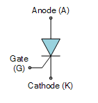
- The silicon-controlled rectifier (SCR) is a three terminal semiconductor switching device which can be used as a controlled switch to perform various functions such as rectification, inversion and regulation of power flow.
- An SCR can handle currents up to several thousand amperes and voltages up to more than 1kV.
- Similar to the diode, SCR is a unidirectional device that conducts current in one direction only, but unlike a diode, the SCR operates as either an open-circuit switch or as a rectifying diode depending upon how its gate is triggered.
- SCR can operate only in the switching mode and cannot be used for amplification.
- Hence, used extensively in switching d.c. And a.c., rectifying a.c
To give controlled output, converting d.c. Into a.c. Etc.
Construction
When a p-n junction is added to a junction transistor, the resulting three p-n junctions’ device is called a silicon-controlled rectifier.
The construction of an SCR. Is as shown in the figure.

Three terminals are:
- The outer p-type material called anode A
- The outer layer of n-type material called cathode K
- The third from the base of transistor section called gate G.
The symbol of SCR is as shown in figure:
Operation:
In SCR the load is connected in series with anode. The anode is always kept at positive potential with respect to cathode.
When gate is open:
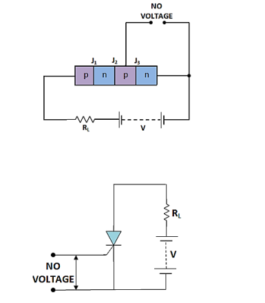
SCR circuit with gate open that is no voltage applied to the gate.
- Under this condition, junction J2 is reverse biased while junction J1 and J3 are forward biased.
- Hence, the situation in the junctions J1 and J3 is an n-p-n transistor with base open.
- Therefore, no current flows through the load RL and SCR is cut-off.
- If the applied voltage is gradually increased, a stage will be reached when the reverse biased junction breaks down and SCR conducts heavily and is said to be ON state.
- The applied voltage at which SCR conducts heavily without the gate voltage is called Break-over voltage.
When the gate voltage is positive with respect to cathode
When a small positive voltage is applied to gate the SCR is made to conduct heavily with respect to the small applied voltage.

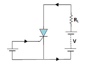
- The electrons from n-type material start to move across junction J3 towards left whereas holes from p-type towards the right.
- Consequently, the electrons from junction J3 are attracted across the junction J2 and gate current starts flowing.
- As soon as the gate current flows, anode current increases.
- The increased current in turn makes more electrons available at junction J2.
- This process continues and in an extremely small time, junction J2 breaks down and the SCR starts conducting heavily.
- Once SCR starts conducting, the gate loses all control. Even if gate voltage is removed, the anode current does not decrease at all.
- The only way to stop conduction to bring the SCR to off condition is to reduce the applied voltage to zero.
Characteristics of SCR
- To obtain V-I characteristics of SCR, its anode and cathode are connected to source through the load.
- The Gate and cathode are fed through a separate source to provide positive gate current from gate to cathode.
- The circuit diagram for obtaining V-I characteristics of SCR is shown in figure.

- The Anode and Cathode terminals A & K are connected to variable voltage source E through Load.
- The Gate terminal G is connected to the source Es to provide positive gate current through G to K when switch S is closed.
- Va and Ia represents the voltage across the anode to cathode terminals and current through the SCR.
- A plot between Va and Ia is drawn by varying the source voltage E and noting the corresponding current through SCR. This plot gives the V-I characteristics of SCR.
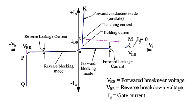 Reverse Blocking Mode
- Reverse Blocking Mode of SCR is that operational mode in which it offers high impedance for current flow and hence do not conduct.
- An SCR in reverse blocking mode behaves as an open switch. Hence, this mode is also known as OFF state of SCR.
- It is shown by OP in the V-I characteristics of SCR.
- From the V-I curve, the anode to cathode voltage is negative in this mode. This means that anode terminal is made negative with respect to cathode with switch S open.
- This leads to reverse biasing of the SCR. Therefore, junction J1 and J3 are reversed biased while the junction J2 is forward biased. The device behaves as if two diodes are connected in series with reverse voltage applies across them.
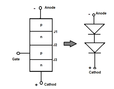
- A small leakage current of the order of milli or micro ampere flows through the SCR in this mode.
- If the reverse voltage is increased, then at some critical voltage an avalanche breakdown takes place at reverse biased junctions J1 and J3 which leads to sudden increase in reverse current.
This critical reverse voltage is called Reverse Breakdown Voltage.
- VBR represents this reverse breakdown voltage in the V-I characteristics.
- There is a sharp increase in reverse current at this voltage. This increased reverse current may result in more losses in the SCR which in turn may damage the SCR.
Forward Blocking Mode
Forward Blocking Mode is the operational mode of SCR in which it does not conduct when forward biased. The term forward biased SCR implies the anode terminal is positive with respect to cathode terminal with gate switch S open.
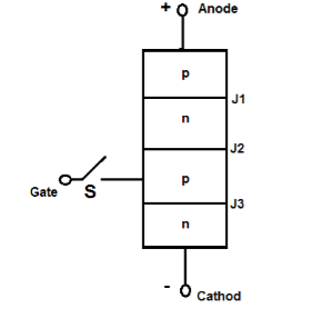
- In this mode, the junction J1 and J3 are forward biased but junction J2 is reverse biased.
A small leakage current, called the forward leakage current, flows as shown by OM in the V-I characteristics of SCR in this mode.
- As the forward leakage current is small, SCR offers high impedance. Therefore, an SCR can be treated as an open switch even in forward blocking mode.
Forward Conduction Mode
There are two possibilities for making SCR to conduct in this mode:
- Increase the anode to cathode voltage to such an extent which leads to avalanche breakdown of the reverse biased junction J2.
- Apply positive gate pulse between gate and cathode terminal.
In forward biasing the voltage is increased then at some critical voltage VBO, an avalanche breakdown take place at reverse biased junction J2. This critical voltage is known as Forward Break over Voltage.
The point M corresponds to Forward Break over Voltage VBO which will at once shift to point N and then to any point in between N and K. Because the anode current in this mode will only be limited by the load, so based on the value of load the anode current will change and may lie at any point in between N and K. Thus, NK represents the forward conduction of SCR.
Ratings of SCR
Thyristor ratings or SCR ratings are required for operating in safe zone. SCR has several ratings such as voltage, current, power, dv/dt, di/ dt, turn on time, turn off time and so on.
Anode voltage rating
This rating provides a brief picture about the withstanding power of thyristor in forward blocking mode in the absence of current.
Peak Working Forward Blocking
It specifies the maximum forward voltage (positive voltage applied across anode and cathode) that can be withstood by SCR at the time of working.
Peak Repetitive Forward Blocking Voltage:
It specifies the peak forward transient voltage that SCR can block repeatedly or periodically in forward blocking mode. This rating is specified at a maximum allowable junction temperature with gate circuit open.
During commutation process, due to high decreasing rate of reverse anode current a voltage spike Ldi/dt is produced which is the cause of VDRM generation.
Peak Non-Repetitive or Surge Forward Blocking Voltage (VDSM)
The peak value of forward transient voltage that does not appear periodically. This type of over voltage is generated at the time of switching operation of circuit breaker.
Peak Working Revere Voltage (VRWM)
It is the maximum reverse voltage which can be withstood by the thyristor repeatedly or periodically.
Peak Repetitive Revere Voltage (VRRM)
It is the value of transient voltage that can be withstand by SCR in reverse bias at maximum allowable temperature. This reason behind the appearance of this voltage is also same as VDRM.
Peak Non-Repetitive Revere Voltage (VRSM)
It implies the reverse transient voltage that does not appear repetitively. Though this voltage value is 130% of VRRM, it lies under reverse break over voltage, VBR.
Forward ON State voltage Drop (VT)
This is the voltage drop across the anode and cathode when rated current flows through
The SCR at rated junction temperature. Generally, this value is lie between 1 to 1.5 volts.
Forward dv/dt Rating
When we apply a forward voltage to the thyristor Junction J1 and J3 are forward biased whereas junction J2 is reverse biased, hence it acts as capacitor. So due to C dv/dt at leakage current flows through the device. This value of current will increase with the value of dv/dt. The reason for leakage is the rate of voltage increasing.
The value of capacitance of the junction is constant hence when dv/dt increases to a suitable value that leakage current occurs and avalanche breakdown across junction J2. This value of dv/dt is called forward dv/dt rating which can turn on the SCR without the help of gate current.
Current ratings of an SCR
The current carrying capability of an SCR is solely determined by the junction temperature
Some of the current ratings are
(i) Forward Current Rating.
The maximum value of anode current, that an SCR can handle safely without any damage, is called the forward current rating. The usual current rating of SCR’s is from 30A to100A. In case the current exceeds the forward current rating, the SCR may get damaged due to intensive heating at the junctions.
(ii) On-state Current.
When the device is in conduction, it carries load current determined
By the supply voltage and load.
On state current is defined in terms of average and rms values. ITav is the
Average value of maximum continuous sinusoidal on state current frequency 40-60 Hz conduction angle 180 which should not exceed with intensive cooling.
(iii) Latching Current
It is the minimum device current which can be attained by the device before the gate drive is removed while turning on for conduction maintenance.
(iv) Holding Current.
It is the minimum on state current required to keep SCR in conducting state without any gate drive. Usually, the value is 5mA
(v) Surge Current.
It is the maximum admissible peak value of a sinusoidal half cycle of 10 ms duration at a frequency of 50 Hz. The value is specified at a given junction temperature. During maximum surge on-state current the junction temperature exceeds temporarily, and forward blocking capabilities are lost for short
Period. The maximum surge on-state current should occur occasionally.
(vi) I2t Value.
It is the time integral of the square of the maximum sinusoidal on-state current. This is usually specified for 3ms to 10ms and determines the thermal rating of the device.
(vii) Critical Rate of Rise of Current.
The maximum rate of increase of current during on-state which the Scr can tolerate is called critical rate of rise of current for the device. This the specified maximum junction temperature.
Applications of SCR:
Application of SCR as static contactor: An important application of SCR is for switching operations. As SCR has no moving parts, therefore, when it is used as a switch, it is often called a static contactor.
Application of SCR for power control: It is often necessary to control power delivered to some load such as the heating element of a furnace. Series resistances or potentiometers cannot be used because they waste power in high power circuits. Under such conditions, silicon-controlled rectifiers are used which are capable of adjusting the transmitted power with little waste.
Application of SCRs for speed control of d.c. Shunt motor: The conventional method of speed control of d.c. Shunt motor is to change the field excitation. But change in field excitation changes the motor torque also. This drawback is overcome in SCR control
Application of SCR Over-light detector: For over light protection the resistor R is a photo-resistor, a device whose resistance decreases with the increase in light intensity. When the light falling on R has normal intensity, the value of R is high enough and the voltage across R1 is insufficient to trigger SCR.
Application of SCR Crowbar: A crowbar is a circuit that is used to protect a voltage-sensitive load from excessive d.c. Power supply output voltages.
References:
1. David. A. Bell (2003), Laboratory Manual for Electronic Devices and Circuits, Prentice Hall, India
2. Santiram Kal (2002), Basic Electronics- Devices, Circuits and IT Fundamentals, Prentice Hall, India
3. Thomas L. Floyd and R. P. Jain (2009), Digital Fundamentals by Pearson Education, 4. Paul B. Zbar, A.P.
Malvino and M.A. Miller (2009), Basic Electronics – A Text-Lab. Manual, TMH
5. R. T. Paynter (2009), Introductory Electronic Devices & Circuits, Conventional Flow
Version, Pearson