Unit - 3
Transistor Amplifiers and Oscillators
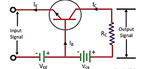
Transistor raises the strength of a weak signal and hence acts an amplifier. The transistor amplifier circuit is shown in the figure below.
Transistor as an Amplifier
The transistor has three terminals namely emitter, base and collector. The emitter and base of the transistor are connected in forward biased and the collector base region is in reverse bias. The forward bias means the P-region of the transistor is connected to the positive terminal of the supply and the negative region is connected to the N-terminal and in reverse bias just opposite of it has occurred.
Vee is applied to the input circuit along with the input signal to achieve the amplification. The DC voltage VEE keeps the emitter-base junction under the forward biased condition regardless of the polarity of the input signal and is known as bias voltage.
When a weak signal is applied to the input, a small change in signal voltage causes a change in emitter current this change is almost the same in collector current because of the transmitter action.
In the collector circuit, a load resistor RC of high value is connected. When collector current flows through such a high resistance, it produces a large voltage drop across it. Thus, a weak signal (0.1V) applied to the input circuit appears in the amplified form (10V) in the collector circuit.
Input Resistance
When the input circuit is forward biased, the input resistance will be low. The input resistance is the opposition offered by the base-emitter junction to the signal flow.
Hence, it is the ratio of small change in base-emitter voltage (ΔVBE) to the resulting change in base current (ΔIB) at constant collector-emitter voltage.
Input resistance, Ri=ΔVBE/ΔIb
Where Ri = input resistance, VBE = base-emitter voltage, and IB = base current.
Output Resistance
The output resistance of a transistor amplifier is very high. The collector current changes very slightly with the change in collector-emitter voltage.
The ratio of change in collector-emitter voltage (ΔVCE) to the resulting change in collector current (ΔIC) at constant base current.
Output resistance = Ro=ΔVCE/ΔIC
Where Ro = Output resistance, VCE = Collector-emitter voltage, and IC = Collector-emitter voltage.
Current gain
It is the ratio of change in collector current (ΔIC) to the change in base current (ΔIB).
Current gain, β=ΔIC/ ΔIB
Voltage Gain
It is the ratio of change in output voltage (ΔVCE) to the change in input voltage (ΔVBE).
Voltage gain, AV=ΔVCE/ΔVBE
ΔIc x RAC/ ΔIB x Ri = ΔIc / ΔIB x RAC/Ri = β x RAC/Ri
Power Gain
It is the ratio of output signal power to the input signal power.
Power gain Ap = (ΔIc) 2 x RAC / (ΔIB) 2 x Ri
ΔIc / ΔIB x R AC / Ri
= current gain x voltage gain
Transistor as oscillator
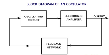
An oscillator must have the following three elements
- Oscillatory circuit or element.
- Amplifier.
- Feedback network.
The oscillatory circuit or element, also called the tank circuit, consists of an inductive coil of inductance L connected in parallel with a capacitor of capacitance C. The frequency of oscillation in the circuit depends upon the values of L and C. The actual frequency of oscillation is the resonant or natural frequency and is given by the expression
f = 1 / 2∏√LC Hz
Where L is inductance of coil in henrys, and C is the capacitance of capacitor in farads.
The oscillations occurring in the tank circuit are applied to the input of the electronic amplifier. Because of the amplifying properties of the amplifier, we get increased output of these oscillations. This amplified output of oscillations is because of dc power supplied from the external source a battery or power supply. The output of the amplifier can be supplied to the tank circuit to meet the losses. The feedback circuit provides positive feedback.
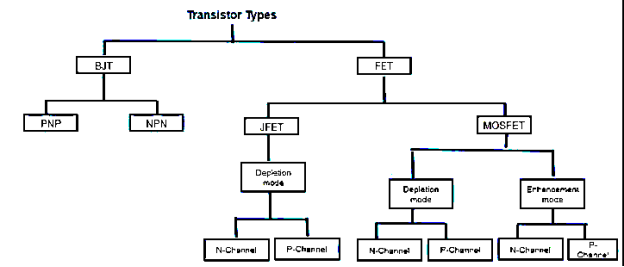
The transistors classification is observed from the above tree diagram. Transistors are basically classified into two types;
Bipolar Junction Transistors (BJT)
Field Effect Transistors (FET).
The BJTs are again classified into NPN and PNP transistors. The FET transistors are classified into JFET and MOSFET.
Junction FET transistors are classified into N-channel JFET and P-channel JFET depending on their function. MOSFET transistors are classified into Depletion mode and Enhancement mode. Again, depletion and enhancement mode transistors are classified into N-channel JFET and P-channel.
- Small Signal Amplifiers are also known as Voltage Amplifiers.
- Voltage Amplifiers have 3 main properties, Input Resistance, Output Resistance and Gain.
- Gain is a ratio of output divided by input, Voltage Gain (Av), Current Gain (Ai) and Power Gain (Ap)
- The power Gain of the amplifier can also be expressed in Decibels or simply dB.
- To amplify the input signal distortion free in a Class A type amplifier, DC Base Biasing is required.
- DC Bias sets the Q-point of the amplifier half- way along the load line.
- This DC Base biasing means that the amplifier consumes power even if there is no input signal present.
- The transistor amplifier is non-linear, and incorrect bias setting will produce large amounts of distortion to the output waveform.
- Too large an input signal will produce large amounts of distortion due to clipping, which is also a form of amplitude distortion.
- Incorrect positioning of the Q-point on the load line will produce either Saturation Clipping or Cut-off Clipping.
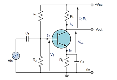
The common emitter amplifier is a three-basic single-stage bipolar junction transistor and is used as a voltage amplifier. The input of this amplifier is taken from the base terminal, the output is collected from the collector terminal and the emitter terminal is common for both the terminals. The basic symbol of the common emitter amplifier is shown below.

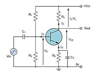
The circuit diagram shows the working of the common emitter amplifier circuit which consists of voltage divider biasing used to supply the base bias voltage as per the necessity. The voltage divider biasing has a potential divider with two resistors connected in a way that the midpoint is used for supplying base bias voltage.
Here R1 resistor is used for the forward bias, the R2 resistor is used for the development of bias, the RL resistor is used at the output it is called as the load resistance. The RE resistor is used for thermal stability. The C1 capacitor is used to separate the AC signals from the DC biasing voltage and the capacitor is known as coupling capacitor.
If R2 resistor increases, then there is an increase in the forward bias. The alternating current is applied to the base of the transistor of the common emitter amplifier circuit then there is a flow of small base current. Hence there is a large amount of current flow through the collector with the help of the RC resistance.
The current gain of the common emitter amplifier is defined as the ratio of change in collector current to the change in base current.
β = ∆ Ic/ ∆ Ib
The voltage gain is defined as the product of the current gain and the ratio of the output resistance of the collector to the input resistance of the base circuits.
Av = β Rc/Rb
Coupling capacitors (or dc blocking capacitors) are used to decouple ac and dc signals so as not to disturb the quiescent point of the circuit when ac signals are injected at the input. Bypass capacitors are used to force signal currents around elements by providing a low impedance path at the frequency.
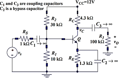
CE amplifier stage
Definition: Distortion in Amplifier basically implies the variation in the waveform received at the output with respect to the applied input. The unwanted alterations generated during amplification is known as distortion.
For an ideal amplifier, the amplified output must be an exact replica of the input. But practically ideal amplifier does not exist. The undesired changes in the signal at the amplifier’s output are termed as distortion in amplifier.

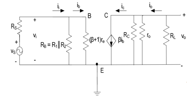
In AC analysis we find
Input resistance or impedance
Output resistance or impedance
Voltage gain
Input resistance
The total resistance at coupling capacitor C1 represents total resistance of the amplifier presented to signal source
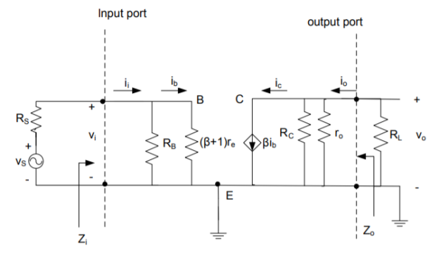
Zi = Vi/I; i = i1 + ib
Vi = I [ RB \\ (β + 1) re
Zi = [ RB \\ (β + 1) re]
Zi = [ R1\\ R2 \\ (β + 1) re]
Output resistance
The total resistance looking into the output of the amplifier at coupling capacitor C2 represents output resistance of the amplifier. To find Zout, input source is set to 0 and test source is applied at output.
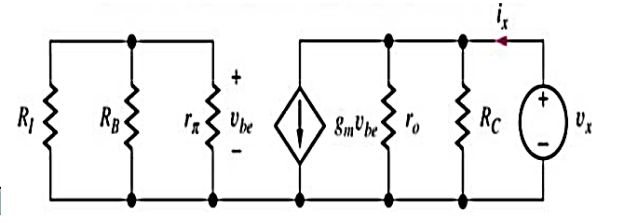
i x = vx / Rc + vx /ro + gm vbe
But vbe is zero. Therefore
Zout = vx/ix = (Rc // ro)
Zout = Rc because ro > Rc
Voltage gain:
Av = vo/vi = -io RL / ib (β + 1) re = - β ib (Rc || ro / Rc ||ro + RL) RL / ib (β + 1) re
Or Av = - β Rc || ro || RL / (β + 1) re
= -Rc ||ro||RL / re
Feedback Amplifier is a device that is based on the principle of feedback. The process by which some part or fraction of output is combined with the input is known as feedback.
Feedback amplifiers are the type of amplifiers in which a part of the output is given back to the input.
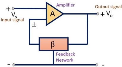
The figure shown below represents the block diagram of an amplifier employing feedback network.
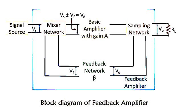
The various blocks of the feedback amplifier section are:
- Signal Source: The signal source can be a voltage source Vs in series with resistor Rs or it can be a current source Is with parallel resistor Rs.
- Feedback network: A feedback network which is a linear two-port network that contains resistors, inductors, capacitors. Its function is to fed back some portion of output to the input.
- Sampling Network: These are basically of two types, current sampling network and voltage sampling network. The output voltage is sampled when we connect feedback network in either shunt or in series with the output.
- Mixer: Mixer circuit is known as the comparator which can be a series mixer or shunt mixer. It mixes the source signal and feedback signal thus produces positive or negative feedback for the device.
The advantages of negative feedback are:
- The negative feedback reduces noise.
- It has highly stabilized gain.
- It can control step response of amplifier.
- It has less harmonic distortion.
- It has less amplitude distortion.
- It has less phase distortion.
- Input and output impedances can be modified as desired.
- It can increase or decrease output impedances.
- It has higher fidelity i.e., more linear operation.
- It has less frequency distortion.
There are four basic amplifier topologies for connecting the feedback signal. Both the current as well as voltage can be feedback toward the input in series otherwise in parallel.
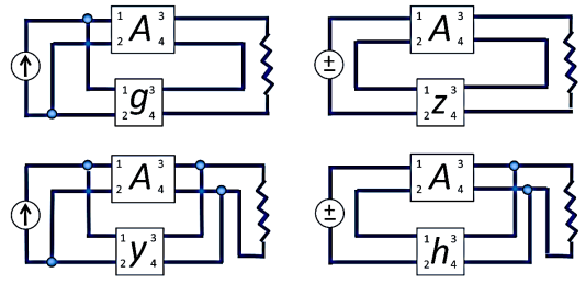
Feedback Amplifier Topologies
- Voltage Series Feedback Amplifier
- Voltage Shunt Feedback Amplifier
- Current Series Feedback Amplifier
- Current Shunt Feedback Amplifier
a.) Voltage Series Feedback Amplifier
In this type of circuit, a portion of the o/p voltage can be applied to the input voltage in series through the feedback circuit. The block diagram of the voltage series feedback-amplifier is shown below.
When the feedback circuit is allied in shunt through the output, then o/p impedance will be reduced and i/p impedance is enlarged because of the series connection with the input.
b.) Voltage Shunt Feedback Amplifier
In this type of circuit, a portion of the o/p voltage can be applied to the input voltage in parallel with through the feedback circuit. The block diagram of the voltage shunt feedback-amplifier is shown below. When the feedback circuit is allied in shunt through the o/p as well as the input, then both the o/p impedance & the i/p impedance will be decreased.
c.) Current Series Feedback Amplifier
In this type of circuit, a portion of the o/p voltage is applied to the i/p voltage in series through the feedback circuit. The block diagram of the current series feedback-amplifier is shown below. When the feedback circuit is allied in series through the o/p as well as the input, then both the o/p impedance & the i/p impedance will be increased.
d.) Current Shunt Feedback Amplifier
In this type of circuit, a portion of the o/p voltage is applied to the i/p voltage in shunt through the feedback circuit. The block diagram of the current shunt feedback-amplifier is shown below.
When the feedback circuit is allied in series through the o/p in parallel with the input, then the o/p impedance will be increased & because of the parallel connection with the i/p, the i/p impedance will be decreased.
In voltage series feedback circuit, a fraction of the output voltage is applied in series with the input voltage through the feedback circuit. This is also known as shunt-driven series-fed feedback, i.e., a parallel-series circuit.
The following figure shows the block diagram of voltage series feedback in which it is evident that the feedback circuit is placed in shunt with the output but in series with the input.
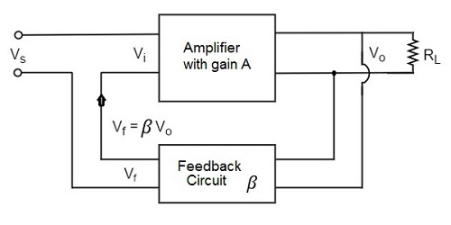
As the feedback circuit is connected in shunt with the output, the output impedance is decreased and due to the series connection with the input, the input impedance is increased.
In the current series feedback circuit, a fraction of the output voltage is applied in series with the input voltage through the feedback circuit. This is also known as series-driven series-fed feedback i.e., a series-series circuit.
The following figure shows the block diagram of current series feedback, by which it is evident that the feedback circuit is placed in series with the output and also with the input.
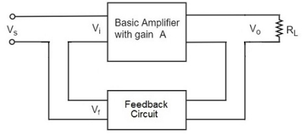
As the feedback circuit is connected in series with the output and the input as well, both the output impedance and the input impedance are increased.
An oscillator provides a source of repetitive A.C. Signal across its output terminals without any need of input. The signal generated by the oscillator is usually of constant amplitude.
The wave shape and amplitude are determined by the design of the oscillator circuit and choice of component values.
The frequency of the output wave may be fixed or variable, depending on the oscillator design.
Oscillators may be classified by the type of signal they produce.
- SINE WAVE OSCILLATORS produce a sine wave output.
- RELAXATION OSCILLATORS and ASTABLE MULTIVIBRATORS produce square waves and rectangular pulses.
- SWEEP OSCILLATORS produce sawtooth waves.
Sine wave oscillators are classified by frequency or the type of frequency control. RF (radio frequency) oscillators work at frequencies above 30 to 50kHz use LC inductors and capacitors or Crystals to control their frequency.
These are classified as HF, VHF, and UHF oscillators, depending on their frequency.
LF (low frequency) oscillators are generally used for generating frequencies below about 30kHz and are usually RC oscillators as they use resistors and capacitors to control their frequency.
Square wave oscillators such as relaxation and a stable oscillator which may be used at any frequency from less than 1Hz up to several GHz which are often implemented in integrated circuit form.
RC Phase shift oscillator

In an RC Oscillator circuit, the input is shifted 180o through the feedback circuit returning the signal out-of-phase and 180o again through an inverting amplifier stage to produces the required positive feedback.
This then gives us “180o + 180o = 360o” of phase shift which is effectively the same as 0o, thereby giving us the required positive feedback.
In other words, the total phase shift of the feedback loop should be “0” or any multiple of 360o to obtain the same effect.

The circuit on the left shows a single resistor-capacitor network whose output voltage “leads” the input voltage by some angle less than 90o.
In a pure or ideal single-pole RC network. It would produce a maximum phase shift of exactly 90o, and because 180o of phase shift is required for oscillation, at least two single-poles networks must be used within an RC oscillator design.
But in reality, it is difficult to obtain exactly 90o of phase shift for each RC stage so we must therefore use more RC stages cascaded together to obtain the required value at the oscillation frequency.
The amount of actual phase shift in the circuit depends upon the values of the resistor (R) and the capacitor (C), at the chosen frequency of oscillations with the phase angle (φ) being given as:
Xc = 1/2π fc R=R
Z = [ R 2 + Xc 2] ½
Ø = tan -1 Xc /R
Wein Bridge Oscillator
Wien bridge oscillator is an audio frequency sine wave oscillator of high stability and simplicity. The feedback signal in this circuit is connected to the non-inverting input terminal so that the op-amp is working as a non-inverting amplifier.
The feedback network does not provide any phase shift. The circuit can be viewed as a Wien bridge with a series combination of R1 and C1 in one arm and parallel combination of R2 and C2 in the adjoining arm. Resistors R3 and R4 are connected in the remaining two arms.
The condition of zero phase shift around the circuit is achieved by balancing the bridge. The series and parallel combination of RC network form a lead-lag circuit.
At high frequencies, the reactance of capacitor C1 and C2 approaches zero. This causes C1 and C2 appears short. Here, capacitor C2 shorts the resistor R2. Hence, the output voltage Vo will be zero since output is taken across R2 and C2 combination. So, at high frequencies, circuit acts as a 'lag circuit'.
At low frequencies, both capacitors act as open because capacitor offers high reactance. Again, output voltage will be zero because the input signal is dropped across the R1 and C1 combination. Here, the circuit acts like a 'lead circuit'.
But at one frequency between the two extremes, the output voltage reaches to the maximum value. At this frequency only, resistance value becomes equal to capacitive reactance and gives maximum output. Hence, this frequency is known as oscillating frequency (f).

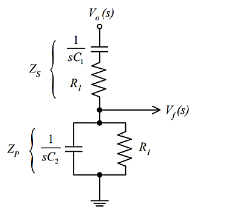
Consider the feedback circuit, on applying voltage divider rule
Vf(s) = Vo(s) x Zp(s)/ Zp(s) + Zs(s)
Zs(s) = R1 + 1/sC1 and Zp(s) = R2|| 1/sC2
Let R1=R2=R and C1=C2=C. On solving
β = Vf(s)/ Vo(s) = RsC /(RsC) 2 + 3RsC + 1 ---------------------------(1)
Since the op-amp is operated in the non-inverting configuration the voltage gain
Av = Vo(s)/ Vf(s) = 1 + R3/R4 -------------------(2)
Applying the condition for sustained oscillations, = Av β =1
RsC /(RsC) 2 + 3RsC + 1. 1 + R3/R4
S=jw
(1 + R3/R4) (jwRC/ - R2 C2 w2 + 3 jwRC + 1) =1
Jw RC (1 + R3/R4) = (- R2 C2 w2 + 3 jwRC + 1)
Jw [(1 + R3/R4) RC – 3RC] = 1- R2 C2 w2
To obtain the frequency of oscillation equate the real part to zero
1-R2 C2 w2 = 0
w = 1/RC
f = 1/ 2 π RC
To obtain the condition for gain at the frequency of oscillation equate the imaginary part to zero.
Jw [(1 + R3/R4) RC – 3RC] = 0
jw [(1 + R3/R4) RC= jw3RC
[(1 + R3/R4) =3
R3/R4 =2
Therefore R3 = 2 R4 is the required condition.
High Frequency LC and Non- Sinusoidal type Oscillators
The LC oscillator consists of an inductor and a capacitor as shown in figure below.
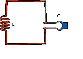
The value of the capacitor and resistor determines the output oscillation. When we apply the voltage, the capacitor gets charged-up. When the supply is cut-off, the stored energy from capacitor flows to inductor and inductor starts building magnetic field around it until the capacitor completely gets discharged.
When the capacitor is fully discharged, the magnetic field around inductor collapse and induces voltage and charge-up the capacitor with opposite polarity and the cycle repeats.
The charge and discharge between L and C produce oscillation and this oscillation is called resonance frequency. However, the frequency generation does last forever due to parasitic resistance which dissipates the energy in the oscillatory circuit in the form of heat.
Non sinusoidal type oscillator
Non-sinusoidal oscillators are oscillators that do not produce a sine-wave output. There is no specific non-sinusoidal waveshape. The non-sinusoidal oscillator output may be a square, sawtooth, rectangular, or triangular waveform or a combination of two wave- forms.
One of the common characteristics of non-sinusoidal oscillators is that they are a form of relaxation oscillator. A relaxation oscillator stores energy in a reactive component during one phase of the oscillation cycle and gradually releases the energy during the relaxation phase of the cycle.

The reason for the name is that the transistor is easily driven into the blocking (cut-off) mode. The blocking condition is determined by the discharge from capacitor C1. Capacitor C1 is charged through the emitter-base junction of transistor Q1.
Once capacitor C1 is charged, the only discharge path is through resistor R1.
The RC time constant of resistor R1 and capacitor C1 determines how long the transistor is blocked, or cut off, as well as determines the oscillator frequency.
A long-time constant produces a low frequency; a short time constant produces a high frequency.
If the output is taken from an RC network in the emitter circuit of the transistor, the output is a saw- tooth waveshape. The RC network determines the frequency of oscillation and produces the sawtooth output.
References:
1. David. A. Bell (2003), Laboratory Manual for Electronic Devices and Circuits, Prentice Hall, India
2. Santiram Kal (2002), Basic Electronics- Devices, Circuits and IT Fundamentals, Prentice Hall, India
3. Thomas L. Floyd and R. P. Jain (2009), Digital Fundamentals by Pearson Education, 4. Paul B. Zbar, A.P.
Malvino and M.A. Miller (2009), Basic Electronics – A Text-Lab. Manual, TMH
5. R. T. Paynter (2009), Introductory Electronic Devices & Circuits, Conventional Flow
Version, Pearson