Unit - 4
Operational Amplifiers and Applications
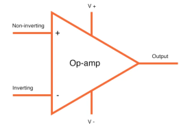
An Operational Amplifier is basically a three-terminal device which consists of two high impedance inputs. One of the inputs is called the Inverting Input, marked with a negative or “minus” sign, (–). The other input is called the Non-inverting Input, marked with a positive or “plus” sign (+).
A third terminal represents the operational amplifiers output port which can both sink and source either a voltage or a current.
In a linear operational amplifier, the output signal is the amplification factor, known as the amplifiers gain (A) multiplied by the value of the input signal and depending on the nature of these input and output signals, there can be four different classifications of operational amplifier gain.
- Voltage – Voltage “in” and Voltage “out”
- Current – Current “in” and Current “out”
- Transconductance – Voltage “in” and Current “out”
- Transresistance – Current “in” and Voltage “out”
The output voltage signal from an Operational Amplifier is the difference between the signals being applied to its two individual inputs.
Op amps are used in a wide variety of applications in electronics. Some of the more common applications are: as a voltage follower, selective inversion circuit, a current-to-voltage converter, active rectifier, integrator, a whole wide variety of filters, and a voltage comparator.
Operational Amplifiers, also known as Op-amps, are basically a voltage amplifying device designed to be used with components like capacitors and resistors, between its in/out terminals.
They form the core part of analog devices. Feedback components are used to determine the operation of the amplifier. The amplifier can perform many different operations resistive, capacitive, or both giving the name Operational Amplifier.

Op-amps are linear devices that are ideal for DC amplification and are used often in signal conditioning, filtering or other mathematical operations.
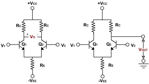
There are four differential amplifier configurations are following:
- Dual input, balanced output differential amplifier.
- Dual input, unbalanced output differential amplifier.
- Single input balanced output differential amplifier.
- Single input unbalanced output differential amplifier.


The configurations are shown in figure which are defined by number of input signals used and the way an output voltage is measured.
If we use two input signals, the configuration is said to be dual input, otherwise it is a single input configuration.
If the output voltage is measured between two collectors, it is referred to as a balanced output because both the collectors are at the same dc potential with respect to ground.
If the output is measured at one of the collectors with respect to ground, the configuration is called an unbalanced output.
A multistage amplifier with a desired gain can be obtained using direct connection between successive stages of differential amplifiers.
The advantage of direct coupling is that it removes the lower cut off frequency imposed by the coupling capacitors, and they are therefore, capable of amplifying dc as well as ac input signals.
If a signal is applied to both inputs of an op amp are equal, then the differential input voltage is unaffected hence the output will not be affected.
In practice, changes in common mode voltage will produce changes in output. The op amp common-mode rejection ratio (CMRR) is the ratio of the common-mode gain to differential-mode gain.
PSRR is the ratio of the change in input offset voltage with respect to the change in power supply voltage.
PSRR=20log (Power Supply Variation)/ (Input Offset Voltage Variation) [dB].
Generally, PSRR is frequency dependent, and decreases as the frequency increases.
Slew rate is defined as the maximum rate of change of an op amp's output voltage and is given units of volts per microsecond. Slew rate is measured by applying a large signal step, such as 1V, to the input of the op amp, and measuring the rate of change from 10% to 90% of the output signal's amplitude.

OPAMP is basically a differential amp that is it will amplify the voltage which is differentially present between its input terminals.
Input stage: The i/p stage is a dual i/p, balanced o/p differential amp. The 2 i/p are inverting and non- inverting i/p terminals. This stage provides most of the voltage gain of the OP-AMP and decides the value of i/p resistance Ri.
Intermediate stage: This is usually another differential amp. The i/p stage drives the stage. The stage is a dual –i/p unbalanced o/p differentiated amp.
Level- shifting stage: Due to direct coupling used between the 1st 2 stages, the i/p of level shifting stage is an amplified signal with some non – zero dc level. Level shifting stage is used to bring dc level to zero volts with respect to gnd.
Output stage: This stage is normally a complementary o/p stage. It increases the magnitude of voltage and raises the current supplying capability of OP-AMP. It also ensures that the o/p resistance of OPAMP is low.
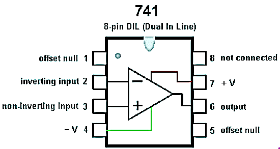
The representation of 741 IC op-amp is given below that comprises of eight pins. The most significant pins are 2,3 and 6, where pin2 and 3 are pin 2 and 3 denote inverting & non-inverting terminals and pin6 denotes output voltage. The triangular form in the IC signifies an op-amp integrated circuit.

It comprises of eight pins where the function of each pin is discussed below.
- Pin-1 is Offset null.
- Pin-2 is Inverting (-) i/p terminal.
- Pin-3 is a non-inverting (+) i/p terminal.
- Pin-4 is -Ve voltage supply (VCC)
- Pin-5 is offset null.
- Pin-6 is the o/p voltage.
- Pin-7 is +ve voltage supply (+VCC)
- Pin-8 is not connected.
In an IC 741 op amp, pin2 and pin6 are the input and output pins. When the voltage is given to the pin-2 then we can get the output from the pin-6. If the polarity of the i/p pin-2 is +Ve, then the polarity which comes from the o/p pin6 is-Ve. So, the o/p is always opposite to the i/p.
Ideal characters of an Op Amp:
1. Open Loop gain
Open loop gain is the gain of the Op Amp without a positive or negative feedback. An ideal OP Amp should have an infinite open loop gain but typically it ranges between 20,000 and 2, 00000.
2. Input impedance
It is the ratio of the input voltage to input current. It should be infinite without any leakage of current from the supply to the inputs. But there will be a few Pico ampere current leakages in most Op Amps.
3. Output impedance
The ideal Op Amp should have zero output impedance without any internal resistance. So that it can supply full current to the load connected to the output.
4. Band width
The ideal Op Amp should have an infinite frequency response so that it can amplify any frequency from DC signals to the highest AC frequencies. But most Op Amps have limited bandwidth.
5. Offset
The output of the Op Amp should be zero when the voltage difference between the inputs is zero. But in most Op Amps, the output will not be zero when off but there will be a minute voltage from it.
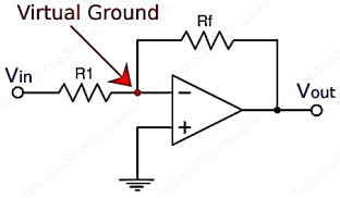
In op-amps virtual ground means that the voltage at that particular node is almost equal to ground voltage (0V). It is useful in analysis of op-amp circuits when negative feedback is employed.
Gain=Vo/Vin
As gain is infinite, Vin = 0
- Vin = V2 – V1
In the above circuit V1 is connected to ground, so V1 = 0. Thus, V2 also will be at ground potential.
V2 = 0

Virtual Ground – Inverting Amplifier
References:
1. David. A. Bell (2003), Laboratory Manual for Electronic Devices and Circuits, Prentice Hall, India
2. Santiram Kal (2002), Basic Electronics- Devices, Circuits and IT Fundamentals, Prentice Hall, India
3. Thomas L. Floyd and R. P. Jain (2009), Digital Fundamentals by Pearson Education, 4. Paul B. Zbar, A.P.
Malvino and M.A. Miller (2009), Basic Electronics – A Text-Lab. Manual, TMH
5. R. T. Paynter (2009), Introductory Electronic Devices & Circuits, Conventional Flow
Version, Pearson