UNIT 2
BJT Circuits
A transistor is an electronic device that can be used as an amplifier or electronic switch. Its ability to amplify the signal or to switch high power loads using a small signal makes it useful in the field of electronics.
There are two basic types of transistors, the bipolar junction transistor, or BJT, and the field-effect transistor, or FET.
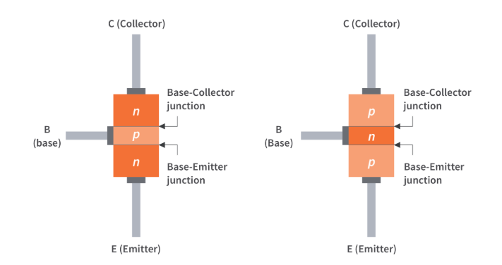
NPN transistor PNP transistor
Figure 1. NPN and PNP transistor
BJT has three terminals Collector (C), Emitter (E) and Base (B). It has a vertically oriented four-layers structure. The vertical structure uses to increase the cross-sectional area.
There are two types of BJT
n-p-n transistor
p-n-p transistor.
It has four layers. The first layer is a heavily doped emitter layer (n+). The second layer is moderately doped the base layer (p). The third region is lightly doped collector drift region (n-). The last layer is a highly doped collector region (n+).
The drift layer (n-) increase the voltage blocking capacity of the transistor due to the low doping level. The width of this layer decides the breakdown voltage.
The power handling capacity of this transistor is very large. So, they have to dissipate power in the form of heat. Sometimes, heat sink is used to increase effective area and therefore increase power dissipation capacity.
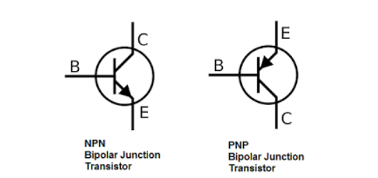
Figure 2. Symbol for NPN and PNP transistor
The I-V characteristic of BJT divides into four regions.
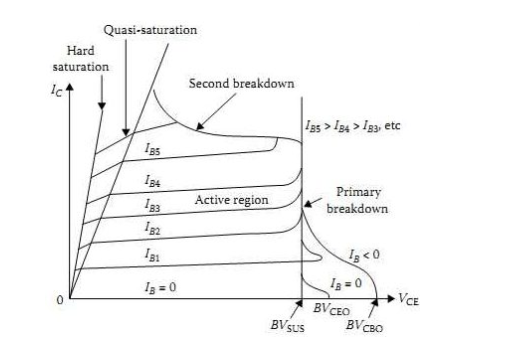
Figure 3. V-I characteristics of BJT
Cut-off region:
The BE and CB both junctions are reverse bias. The base current IB=0 and collector current IC is equal to the reverse leakage current ICEO. The region below the characteristic for IB=0 is cut-off region. In this region, BJT offers large resistance to the flow of current. Hence it is equivalent to an open circuit.
Active region:
The BE junction is forward bias and CB junction is reverse bias. The collector current Ic increase slightly with an increase in the voltage VCE, if IB is increased. The relation of Ib and Ic is,
IC=βdcIB .
If BJT is used as an amplifier or as a series pass transistor in the voltage regulator, it operates in this region. The dynamic resistance in this region is large. The power dissipation is maximum.
Quasi-saturation region:
Quasi-saturation region is between the hard saturation and active region. This region exists due to the lightly doped drift layer. When the BJT operates at high frequency, it is operated in this region. Both junctions are forward bias. The device offers low resistance compared to the active region. So, power loss is less.
In this region, the device does not go into deep saturation. So, it can turn off quickly. Therefore, we can use for higher frequency applications.
Hard-saturation region:
The Power BJT push into the hard-saturation region from the quasi-saturation region by increasing the base current. This region is also known as deep saturation region. The resistance offers in this region is minimum. It is even less than the quasi-saturation region. So, when the BJT operates in this region, power dissipation is minimum. The device acts as a closed switch when it operates in this region. But it needs more time to turn off. So, this region is suitable only for low-frequency switching application. In this region, both junctions are forward bias. The collector current is not proportional to the base current, IC remains almost constant at IC(sat) and independent from the value of base current.
Suppose we had a lamp that we wanted to turn on and off with a switch. Such a circuit would be extremely simple, as in the figure below.

a- mechanical switch
b- NPN transistor switch
c- PNP transistor switch
Figure 4. transistor as switch
Suppose we insert a transistor in place of the switch to show how it can control the flow of electrons through the lamp. Remember that the controlled current through a transistor must go between collector and emitter.

Figure 5. Transistor: a) cut-off lamp b) saturated, lamp on.
The choice between NPN and PNP is really arbitrary. All that matters is that the proper current directions are maintained for the sake of correct junction biasing.
In the above figures, the base of either BJT is not connected to a suitable voltage, and no current is flowing through the base. Consequently, the transistor cannot turn on. Therefore, connect a switch between the base and collector wires of the transistor as in figure.
If the switch is open as in figure (a), the base wire of the transistor will be left “floating” and there will be no current through it. In this state, the transistor is said to be cut-off.
If the switch is closed as in figure (b), current will be able to flow from the base to the emitter of the transistor through the switch. This base current will enable a much larger current flow from the collector to the emitter, thus lighting up the lamp. In this state of maximum circuit current, the transistor is said to be saturated.
Transistor raises the strength of a weak signal and hence acts an amplifier. The transistor amplifier circuit is shown in the figure below.
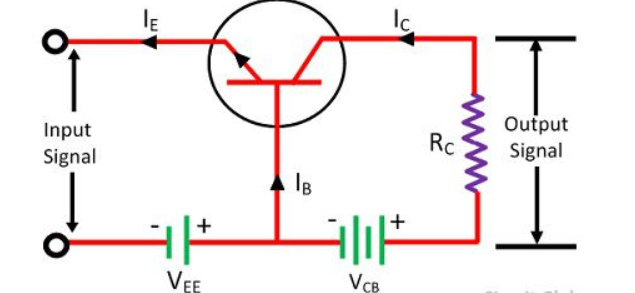
Figure 6. Transistor as an Amplifier
The transistor has three terminals namely emitter, base and collector. The emitter and base of the transistor are connected in forward biased and the collector base region is in reverse bias. The forward bias means the P-region of the transistor is connected to the positive terminal of the supply and the negative region is connected to the N-terminal and in reverse bias just opposite of it has occurred.
Vee is applied to the input circuit along with the input signal to achieve the amplification. The DC voltage VEE keeps the emitter-base junction under the forward biased condition regardless of the polarity of the input signal and is known as bias voltage.
When a weak signal is applied to the input, a small change in signal voltage causes a change in emitter current this change is almost the same in collector current because of the transmitter action.
In the collector circuit, a load resistor RC of high value is connected. When collector current flows through such a high resistance, it produces a large voltage drop across it. Thus, a weak signal (0.1V) applied to the input circuit appears in the amplified form (10V) in the collector circuit.
Input Resistance
When the input circuit is forward biased, the input resistance will be low. The input resistance is the opposition offered by the base-emitter junction to the signal flow.
Hence, it is the ratio of small change in base-emitter voltage (ΔVBE) to the resulting change in base current (ΔIB) at constant collector-emitter voltage.
Input resistance, Ri=ΔVBE/ΔIb
Where Ri = input resistance, VBE = base-emitter voltage, and IB = base current.
Output Resistance
The output resistance of a transistor amplifier is very high. The collector current changes very slightly with the change in collector-emitter voltage.
The ratio of change in collector-emitter voltage (ΔVCE) to the resulting change in collector current (ΔIC) at constant base current.
Output resistance = Ro=ΔVCE/ΔIC
Where Ro = Output resistance, VCE = Collector-emitter voltage, and IC = Collector-emitter voltage.
Current gain
It is the ratio of change in collector current (ΔIC) to the change in base current (ΔIB).
Current gain, β=ΔIC/ ΔIB
Voltage Gain
It is the ratio of change in output voltage (ΔVCE) to the change in input voltage (ΔVBE).
Voltage gain, AV=ΔVCE/ΔVBE

Power Gain
It is the ratio of output signal power to the input signal power.
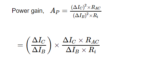
= current gain x voltage gain
The hybrid pi model of a BJT is a small signal model, named after the “p”-like equivalent circuit for a bipolar junction transistor. The model is shown in figure. It consists of an input impedance, rp, an output impedance r0, and a voltage controlled current source described by the transconductance, gm. In addition it contains the base-emitter capacitances, the junction capacitance, Cj,BE, and the diffusion capacitance, Cd,BE, and the base-collector junction capacitance, Cj,BC, also referred to as the Miller capacitance. |

Figure 7. Small signal hybrid model of BJT
The transconductance, gm, of a bipolar transistor is defined as the change in the collector current divided by the change of the base-emitter voltage.
 ------------------------(1)
The base input resistance, rp, is defined as the change of the emitter-base voltage divided by the change of the base current.
 --------------------(2)
The output resistance, ro, is defined as:
 --------------------------------(3)
The base-emitter and base-collector junction capacitances are given by:
 ---------------------------------------(4)
 ------------------------------------(5)
for the case where the base-emitter and base-collector junctions are abrupt. Since the base-emitter is strongly forward biased in the forward active mode of operation, one has to also include the diffusion capacitance of the base:
 -----------------------------------------------(6)
Based on the small signal model shown in Figure we can now calculate the small signal current gain versus frequency, hfe, of a BJT biased in the forward active mode and connected in a common emitter configuration. The maximum current gain is calculated while shorting the output, resulting in:
 ------------------(7)
The unity gain frequency, fT, also called the transit frequency is obtained by setting the small signal current gain, hfe, equals to one, resulting in:
 ----------------------------------(8)
This transit frequency can be expressed as a function of the transit time, t:
 -----------------------(9)
Where the transit time, t, equals:
 -------------------(10)
The circuit model therefore includes the charging time of the base-emitter capacitance, tE, as well as the base transit time, tB, but not the transit time of the carriers through the base-collector depletion region, tC.
The collector transit time is
 -----------------------------------------(11)
The total transit time is given by
 --------------(12)
The maximum oscillation frequency, fMAX, is linked to the transit frequency, fT, and is obtained from:
Where RB is the total base resistance and Cj,BC is the base-collector capacitance. |
Biasing refers to the application of dc voltages to establish a fixed level of current and voltage. The proper flow of zero signal collector current and maintenance of proper collector emitter voltage for the passage of signal is called Transistor Biasing. The circuit which provides transistor biasing is called Biasing circuit.
The need for biasing circuit is that if a signal of low voltage is given as input it has to amplify and meet these two conditions:
Transistor Regions Operation:
Base–emitter junction forward-biased
Base–collector junction reverse-biased
2. Cutoff-region operation:
Base–emitter junction reverse-biased
Base–collector junction reverse-biased
3. Saturation-region operation:
Base–emitter junction forward-biased
Base–collector junction forward-biased
Types of Bias
In fixed bias since it is C-E configuration
1st step: Locate capacitors and replace them with an open circuit
2nd step: Locate 2 main loops
BE loop (input loop)
CE loop(output loop)
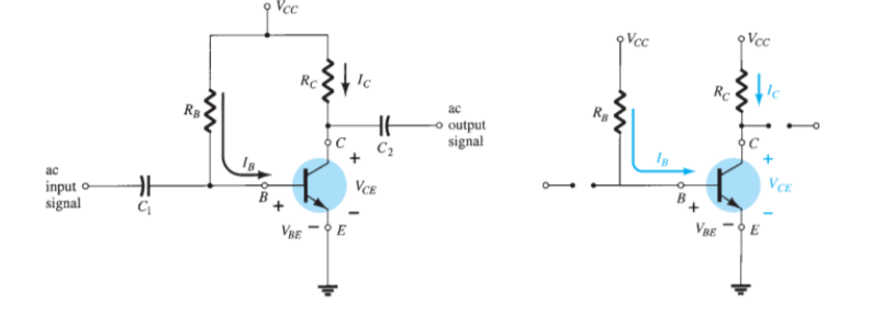
Base – emitter loop

Collector emitter loop
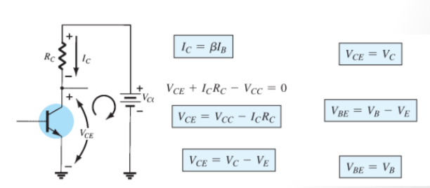
Problem:
Determine the following for the fixed bias configuration:
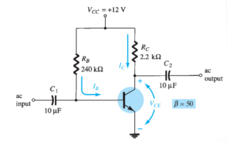
i) IBQ and ICQ
ii) VCE Q
iii) VB and VC
iv) VBC
IBQ = Vcc – Bbe/Rb = 12 – 0.7/ 240K = 47.08 µ A
ICQ = β I BQ = (50) ( 47.08 µ) = 2.35 mA
VCE Q = VCC – Ic Rc
= 12 – (2.35 mA)(2.2 KΩ)
= 6.83 V
VB = VBE = 0.7 V
VC = VCE = 6.83 V
Using double -subscript notation yields
VBC = VB – VC = 0.7 V – 6.83 V = -6.13 V
The negative sign reveals that the junction is reverse biased as it should be for linear amplification.
Transistor Saturation
a) Actual b) Approximate
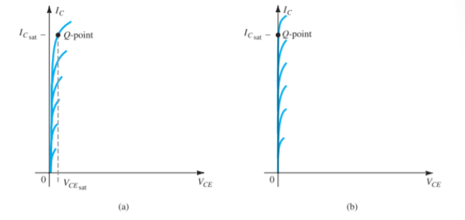
IC (sat)

Fixed bias configuration

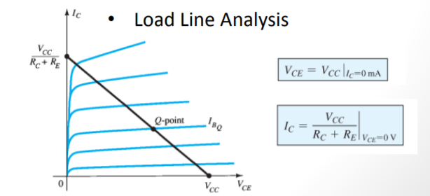
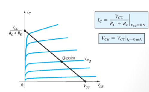
Load Line Analysis
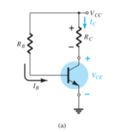

(a) – circuit
(b) Characteristics
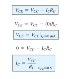

Emitter bias Configuration
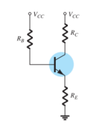
BJT bias circuit with emitter resistor.
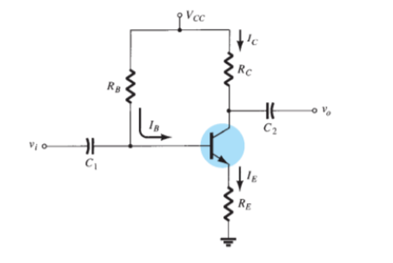
DC equivalent
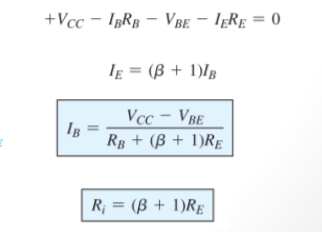
Base – Emitter loop

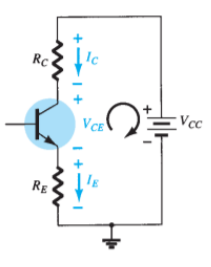
Collector -Emitter configuration

Problem :
For the emitter-bias network find the following:
a) IB
b) IC
c) VCE
d) VC
e) VE
f) VB
g) VBC
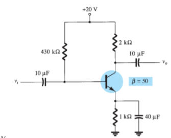
I B = Vcc – VBE/ RB + (β +1) RE = 20 V – 0.7V / 430k Ω + (51)(1kΩ) = 40.1 μ A
Ic = β Ib
= (50) ( 40.1 μ A )
= 2.01 mA
VCE = VCC – Ic( RC + RE)
= 20 V – (2.01mA)(2kΩ + 1kΩ)
= 13.97 V
Vc = Vcc – Ic Rc
= 20 V – (2.01mA)(2kΩ)
= 15.98 V
VE = IE RE = 2.01 m A x 1 k Ω
= 2.01 V
VB = VBE + VE
= 0.7 + 2.01 V = 2.71 V
VBC = VB – VC = 2.71 – 15.98 = -13.27 V
The addition of the emitter resistor to the dc bias of the BJT provides improved stability, that is, the dc bias currents and voltages remain closer to where they were set by the circuit when outside conditions, such as temperature and transistor beta, change.
Saturation level
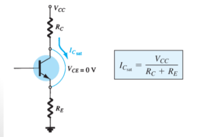
Load Line Analysis
Approximate analysis
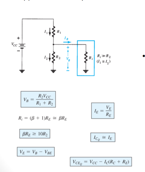
Transistor Analysis

Load Line Analysis
Determine the levels of ICQ and VCEQ for voltage divider configuration using exact and approximate techniques and compare solutions.
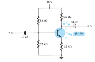
β . RE ≥ 10 R2
(50)(1.2 k Ω) ≥ 10(22 k Ω)
 60kΩ ≥ 220kΩ
Rth = R1 || R2 82 kΩ || 22 kΩ = 17.35 kΩ
Eth = R2 Vcc/ R1 + R2 = 22kΩ (18V)/ 82kΩ + 22kΩ = 3.81 V
IB = Eth – VBE/ Rth + (β +1) RE = 3.81 V – 0.7V / 17.35 kΩ + (51 )(1.2kΩ) = 3.11/ 78.55 kΩ = 39.6 μ A
ICQ = β IB = (50)(39.6μA) = 1.98 mA
VCEQ = Vcc – IC(RC + RE)
= 18V – (1.98mA)(5.6kΩ + 1.2 kΩ)= 4.54V
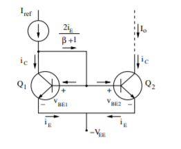
Consider the circuit shown with identical transistors, Q1 and Q2. Because both bases and emitters of the transistors are connected together, KVL leads to vBE1 = vBE2. BJT operation is controlled by vBE. As vBE1 = vBE2 and transistors are identical, they should have similar iE, iB and ic:
iB = iE/ β + 1 Io = ic = β iE/ β + 1
KCL = I ref = ic + 2 iE/ β + 1 = iE/ β + 1 + 2 iE/ β + 1= β + 2/ β + 1 . iE
Io/Iref = β / β + 2 = 1/ 1+2/β
For β >> 1, Io ≈ Iref (with an accurancy of 2/β). This circuit is called a “current mirror” as the two transistors work in tandem to ensure that current Io remains the same as Iref no matter what circuit is attached to the collector of Q2. As such, the circuit behaves as a current source and can be used to bias BJT circuits.
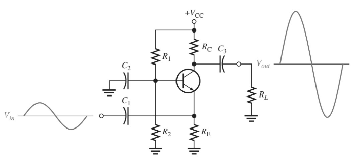
The common emitter amplifier is a three basic single-stage bipolar junction transistor and is used as a voltage amplifier. The input of this amplifier is taken from the base terminal, the output is collected from the collector terminal and the emitter terminal is common for both the terminals. The basic symbol of the common emitter amplifier is shown below.
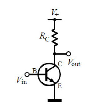
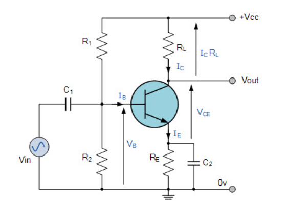
The circuit diagram shows the working of the common emitter amplifier circuit which consists of voltage divider biasing used to supply the base bias voltage as per the necessity. The voltage divider biasing has a potential divider with two resistors connected in a way that the midpoint is used for supplying base bias voltage.
Here R1 resistor is used for the forward bias, the R2 resistor is used for the development of bias, the RL resistor is used at the output it is called as the load resistance. The RE resistor is used for thermal stability. The C1 capacitor is used to separate the AC signals from the DC biasing voltage and the capacitor is known as coupling capacitor.
If R2 resistor increases, then there is an increase in the forward bias. The alternating current is applied to the base of the transistor of the common emitter amplifier circuit then there is a flow of small base current. Hence there is a large amount of current flow through the collector with the help of the RC resistance.
The voltage near the resistance RC will change because the value is very high and the values are from the 4 to 10kohm. Hence there is a huge amount of current present in the collector circuit which amplified from the weak signal, therefore common emitter transistor work as an amplifier circuit.
The current gain of the common emitter amplifier is defined as the ratio of change in collector current to the change in base current.
β = ∆ Ic/ ∆ Ib
The voltage gain is defined as the product of the current gain and the ratio of the output resistance of the collector to the input resistance of the base circuits.
Av = β Rc/Rb
Characteristics
Applications of Common Emitter Amplifier
Common Base Amplifier has the following:
The common base amplifier circuit consists of voltage divider bias configuration.
Base of the BJT is the common terminal and is at AC ground due to the capacitor. The input signal is given to the emitter through capacitor coupling. Output is taken at the collector and the load is capacitively coupled to the collector.
In order to determine the characteristics, we need to construct an AC equivalent model of the common base amplifier.

Voltage Gain
The voltage gain of CB amplifier from emitter (input) to collector (output) is given by
AV = Vout / Vin = Vc / Ve = Ic Rc / Ie (r’e || RE) ≈ Ie Rc / Ie (r’e || RE)
Assuming RE >> r’e, then AV ≈ Rc / r’e
Here, Rc = RC || RL
r’e = AC Emitter Resistance
the voltage gain of a common base amplifier is very high without the phase inversion.
Current GainThe current gain of CB amplifier is output current divided by the input current. From AC equivalent mode, Ic is the output current and Ie is the input current.
Since Ic ≈ Ie, the current gain Ai ≈ 1.
Input ResistanceThe input resistance is the equivalent resistance looking it at the emitter. It is given by
Rin = Vin / Iin = Ve / Ie = Ie (r’e || RE) / Ie = r’e || RE
Usually, RE is much greater than r’e.
If RE >> r’e, then Rin ≈ r’e.
This means that the input resistance of a common base amplifier is usually very low.
Output ResistanceThe output resistance is the Thevenin equivalent at the output of the common base amplifier looking back into the amplifier. The AC collector resistance r’c is in parallel with RC and it is usually much larger than RC.
Hence, Rout ≈ RC

Resistors R1 and R2 form a simple voltage divider network used to bias the NPN transistor into conduction. Since this voltage divider lightly loads the transistor, the base voltage, VB can be easily calculated by using the simple voltage divider formula as shown.
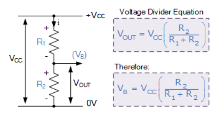
With the collector terminal of the transistor connected directly to VCC and no collector resistance, (RC = 0) any collector current will generate a voltage drop across the emitter resistor RE.
However, in the common collector amplifier circuit, the same voltage drop, VE also represents the output voltage, VOUT. RE depends greatly on IB and the transistors current gain Beta, β.
As the base-emitter pn-junction is forward biased, base current flows through the junction to the emitter encouraging transistor action causing a much larger collector current, IC to flow.
Thus, the emitter current is a combination of base current and collector current as: IE = IB + IC.
However, as the base current is extremely small compared to the collector current, the emitter current is therefore approximately equal to the collector current. Thus IE ≈ IC
As the amplifiers output signal is taken from across the emitter load this type of transistor configuration is also known as an Emitter Follower circuit as the emitter output “follows” or tracks any voltage changes to the base input signal. Thus, VIN and VOUT are in-phase producing zero phase difference between the input and output signals.
Voltage gain:
Vout = Vin x RE/ r’e + RE
Thus Av = Vout/ Vin = Ie x RE/ Ie(r’e + RE)
Since RE is much greater than r’e (r’e + RE) ≈ RE
And the two emitter currents cancel out
Av = Vout/Vin = RE/RE ≈ 1
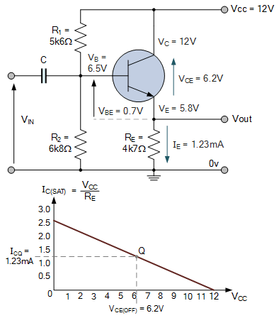
A common collector amplifier is constructed using an NPN bipolar transistor and a voltage divider biasing network. If R1 = 5k6Ω, R2 = 6k8Ω and the supply voltage is 12 volts. Calculate the values of: VB, VC and VE, the emitter current IE, the internal emitter resistance r’e and the amplifiers voltage gain AV when a load resistance of 4k7Ω is used. Also draw the final circuit and corresponding characteristics curve with load line.
Base biasing voltage, VB
I = VCC/ R1 + R2 = 12/ 5600 + 6800 = 968 µ A
VB = I x R2 = 968 x 10 -6 x 6800 = 6.5 V
Collector voltage, VC. As there is no collector load resistance, the transistors collector terminal is connected directly to the DC supply rail, so VC = VCC = 12 volts.
Emitter biasing voltage, VE
VE = VB – VBE = 6.5 – 0.7 = 5.8 V
Thus
VCE(off) = VCC – VE = 12 – 5.8 = 6.2 V
Emitter Current, IE
IE = VE/RE = 5.8 / 4700 = 1.23 mA
AC Emitter Resistance, r’e
r’e = 25mV/IE = 25mV/1.23mA = 20.3 Ω
Voltage gain, AV
Av = RE/ re + RE = 4700/ 20.3 + 4700 = 99.6%
The BJT small-signal models are drop-in replacements for the BJT symbol in a circuit diagram. Once the bias conditions are determined remove the BJT and insert the small-signal model, and connect the previous base, collector, and emitter nodes to the model’s base, collector, and emitter terminals.
The next step is to replace each DC voltage source with a short circuit and each DC current source with an open circuit, because this corresponds to the behaviour in context of small-signal operation.
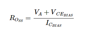
In small-signal the variable that affects the collector current is the base current, the emitter current, or the base-to-emitter voltage. If we want the small-signal models to be more accurate, we need to account for the Early effect. Hence, a resistor connected between the collector and the emitter.
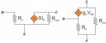
This resistor represents the small-signal output resistance, which is calculated as follows:

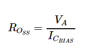
The Early voltage (VA) will often be significantly larger than the collector-to-emitter voltage, so you can simplify this as follows:

Ci = cwi + cbe + cbc( 1-av) Co = cwo + cce + cbc( 1-AV)
= cwi + cbe + cmi = cwo + cce + cmo
Where cmi = input miller capacitance where cmo = o/p miller capacitance
At increasing frequencies, the reactance xc will decrease in magnitude resulting in a shorting effect across the output and a decrease in gain.
For high frequency response, various parasite capacitances (cbe, cbc, cce) of the transistors are included along with the wiring capacitors ( cwi, cwo) for analysis.
For high frequency response, cs, cc, ce are assumed to be in short circuit state.
Input capacitance ci includes wiring capacitance cwi, the transistor capacitance.
Cbe and miller capacitance cmi.
The o/p capacitance co includes wiring cce and miller capacitance cmo
Cmi = cbc (1-av)
Cmo = cbc (1−11−1/av)

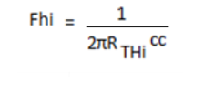
For the input network, the – 3db frequency is defined by

rthi = rsrs // r1r1 // r2r2 // rππ
ci = cwi + cbc + cmi
cmi = cbc (1-av)
at very high frequency, the effect of ci is to reduce the total impedance of the parallel combination of r1r1, r2r2 , rπrπ & ci. The route is a reduced level of voltage across ci, a reduction in In and a gain for the system.
Rtho = rc // rlrl // re
c0c0 = cwot + cce + cmo
Cme = cbe ( 1 - 1av)1av)
∵∵ 1 >> yav cmo = cbc
At very high frequency, XCO will decrease and consequently reduced the total impedance of o/p parallel branches. The net result is vo will also decline towards ‘o’ as the reactance xc becomes (zero) or smaller.
References:
2. Electronic Devices and Circuits by VENKATA RAO, McGraw Hill
3. Microelectronic circuits by Smith
4. Analog Electronic circuits by A.P Godse
5. Analog Electronic circuits by J.B Gupta.

