UNIT - 4
Memory organization
Abstraction is one of the most important aspects of computing. It is a widely implemented Practice in the Computational field.
Memory Interleaving is less or More an Abstraction technique. Though it's a bit different from Abstraction. It is a Technique that divides memory into several modules such that Successive words in the address space are placed in the Different module.
Consecutive Word in a Module:
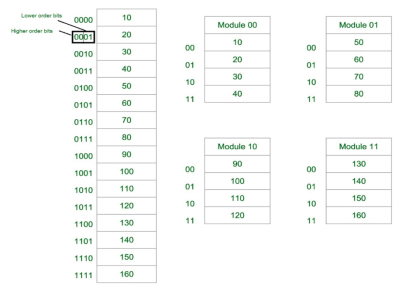
Fig-1: Consecutive Word in a Module
Let us assume 16 Data’s to be Transferred to the Four Module. Where Module 00 be Module 1, Module 01 be Module 2, Module 10 be Module 3 & Module 11 be Module 4. Also, 10, 20, 30….130 are the data to be transferred.
From the figure above in Module 1, 10 [Data] is transferred then 20, 30 & finally, 40 which are the Data. That means the data are added consecutively in the Module till its max capacity.
The most significant bit (MSB) provides the Address of the Module & the least significant bit (LSB) provides the address of the data in the module.
For Example, to get 90 (Data) 1000 will be provided by the processor. This 10 will indicate that the data is in module 10 (module 3) & 00 is the address of 90 in Module 10 (module 3). So,
Module 1 Contains Data : 10, 20, 30, 40
Module 2 Contains Data : 50, 60, 70, 80
Module 3 Contains Data : 90, 100, 110, 120
Module 4 Contains Data : 130, 140, 150, 160
Consecutive Word in Consecutive Module:
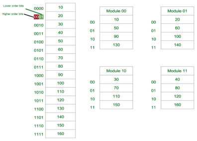
Fig-2: Consecutive Word in Consecutive Module
Now again we assume 16 Data’s to be transferred to the Four Module. But Now the consecutive Data are added in the Consecutive Module. That is, 10 [Data] is added in Module 1, 20 [Data] in Module 2 and So on.
The Least Significant Bit (LSB) provides the Address of the Module & the Most significant bit (MSB) provides the address of the data in the module.
For Example, to get 90 (Data) 1000 will be provided by the processor. This 00 will indicate that the data is in module 00 (module 1) & 10 is the address of 90 in Module 00 (module 1). That is,
Module 1 Contains Data : 10, 50, 90, 130
Module 2 Contains Data : 20, 60, 100, 140
Module 3 Contains Data : 30, 70, 110, 150
Module 4 Contains Data : 40, 80, 120, 160
Why we use Memory Interleaving? [Advantages]:
Whenever Processor requests Data from the main memory. A block (chunk) of Data is Transferred to the cache and then to Processor. So whenever a cache miss occurs the Data is to be fetched from the main memory. But main memory is relatively slower than the cache. So to improve the access time of the main memory interleaving is used.
We can access all four Modules at the same time thus achieving Parallelism. From Figure 2 the data can be acquired from the Module using the Higher bits. This method Uses memory effectively.
Types of Memory Interleaving
Memory Interleaving is an abstraction technique that divides memory into some modules such that successive words in the address space are placed in the different modules.
Suppose a 64 MB memory made up of the 4 MB chips as shown in the below:
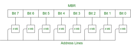
Fig 3 - Example
We organize the memory into 4 MB banks, each having eight of the 4 MB chips. The memory thus has 16 banks, each of 4 MB.
64 MB memory = 2^26, so 26 bits are used for addressing.
16 = 2^4, so 4 bits of the address select the bank, and 4 MB = 2^22, so 22 bits of the address to each chip.
In general, an N-bit address, with N = L + M, is broken into two parts:
When one of the memory banks is active, the other (2L – 1) are inactive. All banks receive the M-bit address, but the inactive ones do not respond to it.
Classification of Memory Interleaving:
Memory interleaving is classified into two types:
1. High Order Interleaving –
In high-order interleaving, the most significant bits of the address select the memory chip. The least significant bits are sent as addresses to each chip. One problem is that consecutive addresses tend to be in the same chip. The maximum rate of data transfer is limited by the memory cycle time.
It is also known as Memory Banking.
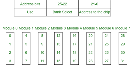
Fig 4 – Memory banking
2. Low Order Interleaving –
In low-order interleaving, the least significant bits select the memory bank (module). In this, consecutive memory addresses are in different memory modules. This allows memory access at much faster rates than allowed by the cycle time.
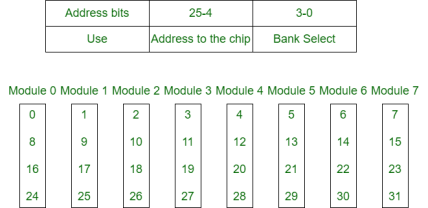
Fig 5 – low order interleaving memory bank
Key takeaway
Abstraction is one of the most important aspects of computing. It is a widely implemented Practice in the Computational field.
Memory Interleaving is less or More an Abstraction technique. Though it's a bit different from Abstraction. It is a Technique that divides memory into several modules such that Successive words in the address space are placed in the Different module.
A memory unit is an essential component in any digital computer since it is needed for storing programs and data.
Typically, a memory unit can be classified into two categories:
Apart from the basic classifications of a memory unit, the memory hierarchy consists of all of the storage devices available in a computer system ranging from the slow but high-capacity auxiliary memory to relatively faster main memory.
The following image illustrates the components in a typical memory hierarchy.
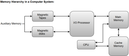
Fig 6 – Memory hierarchy in a computer system
Auxiliary memory is known as the lowest-cost, highest-capacity, and slowest-access storage in a computer system. Auxiliary memory provides storage for programs and data that are kept for long-term storage or when not in immediate use. The most common examples of auxiliary memories are magnetic tapes and magnetic disks.
A magnetic disk is a digital computer memory that uses a magnetization process to write, rewrite and access data. For example, hard drives, zip disks, and floppy disks.
Magnetic tape is a storage medium that allows for data archiving, collection, and backup for different kinds of data.
The main memory in a computer system is often referred to as Random Access Memory (RAM). This memory unit communicates directly with the CPU and with auxiliary memory devices through an I/O processor.
The programs that are not currently required in the main memory are transferred into auxiliary memory to provide space for currently used programs and data.
The primary function of an I/O Processor is to manage the data transfers between auxiliary memories and the main memory.
The data or contents of the main memory that are used frequently by the CPU are stored in the cache memory so that the processor can easily access that data in a shorter time. Whenever the CPU requires accessing memory, it first checks the required data into the cache memory. If the data is found in the cache memory, it is read from the fast memory. Otherwise, the CPU moves onto the main memory for the required data.
Key takeaway
A memory unit is an essential component in any digital computer since it is needed for storing programs and data.
Typically, a memory unit can be classified into two categories:
The data or contents of the main memory that are used frequently by the CPU are stored in the cache memory so that the processor can easily access that data in a shorter time. Whenever the CPU needs to access memory, it first checks the cache memory. If the data is not found in the cache memory, then the CPU moves into the main memory.
Cache memory is placed between the CPU and the main memory. The block diagram for a cache memory can be represented as:

Fig 7 – Cache memory
The cache is the fastest component in the memory hierarchy and approaches the speed of CPU components.
The basic operation of cache memory is as follows:
Cache Memory is a special very high-speed memory. It is used to speed up and synchronizing with a high-speed CPU. Cache memory is costlier than main memory or disk memory but economical than CPU registers. Cache memory is an extremely fast memory type that acts as a buffer between RAM and the CPU. It holds frequently requested data and instructions so that they are immediately available to the CPU when needed.
Cache memory is used to reduce the average time to access data from the Main memory. The cache is a smaller and faster memory that stores copies of the data from frequently used main memory locations. There are various independent caches in a CPU, which store instructions and data.

Fig 8 - Memory
Levels of memory:
It is a type of memory in which data is stored and accepted that are immediately stored in the CPU. The most commonly used register is accumulator, Program counter, address register, etc.
It is the fastest memory which has faster access time where data is temporarily stored for faster access.
It is the memory on which the computer works currently. It is small in size and once power is off data no longer stays in this memory.
It is external memory that is not as fast as main memory but data stays permanently in this memory.
Cache Performance:
When the processor needs to read or write a location in the main memory, it first checks for a corresponding entry in the cache.
The performance of cache memory is frequently measured in terms of a quantity called the Hit ratio.
Hit ratio = hit / (hit + miss) = no. of hits/total accesses
We can improve Cache performance using higher cache block size, higher associativity, reduce miss rate, reduce miss penalty, and reduce the time to hit in the cache.
Cache Mapping:
There are three different types of mapping used for cache memory which are as follows: Direct mapping, Associative mapping, and Set-Associative mapping. These are explained below.
The simplest technique, known as direct mapping, maps each block of main memory into only one possible cache line. or
In Direct mapping, assign each memory block to a specific line in the cache. If a line is previously taken up by a memory block when a new block needs to be loaded, the old block is trashed. An address space is split into two parts index field and a tag field. The cache is used to store the tag field whereas the rest is stored in the main memory. Direct mappings performance is directly proportional to the Hit ratio.
2. i = j modulo m
3. where
4. i=cache line number
5. j= main memory block number
m=number of lines in the cache
For purposes of cache access, each main memory address can be viewed as consisting of three fields. The least significant w bits identify a unique word or byte within a block of main memory. In most contemporary machines, the address is at the byte level. The remaining s bits specify one of the 2s blocks of main memory. The cache logic interprets these s bits as a tag of s-r bits (most significant portion) and a line field of r bits. This latter field identifies one of the m=2r lines of the cache.

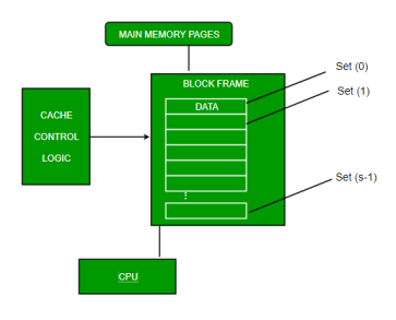
Fig 9 – Direct mapping
2. Associative Mapping –
In this type of mapping, the associative memory is used to store content and addresses of the memory word. Any block can go into any line of the cache. This means that the word id bits are used to identify which word in the block is needed, but the tag becomes all of the remaining bits. This enables the placement of any word at any place in the cache memory. It is considered to be the fastest and the most flexible mapping form.
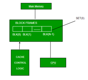
Fig 10 – Associative mapping
3. Set-associative Mapping –
This form of mapping is an enhanced form of direct mapping where the drawbacks of direct mapping are removed. Set associative addresses the problem of possible thrashing in the direct mapping method. It does this by saying that instead of having exactly one line that a block can map to in the cache, we will group a few lines creating a set. Then a block in memory can map to any one of the lines of a specific set. Set-associative mapping allows that each word that is present in the cache can have two or more words in the main memory for the same index address. Set associative cache mapping combines the best of direct and associative cache mapping techniques.
In this case, the cache consists of several sets, each of which consists of several lines. The relationships are
m = v * k
i= j mod v
where
i=cache set number
j=main memory block number
v=number of sets
m=number of lines in the cache number of sets
k=number of lines in each set

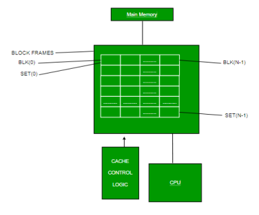
Fig 11 – Set associative mapping
Application of Cache Memory –
Types of Cache –
A primary cache is always located on the processor chip. This cache is small and its access time is comparable to that of processor registers.
2. Secondary Cache –
Secondary cache is placed between the primary cache and the rest of the memory. It is referred to as the level 2 (L2) cache. Often, the Level 2 cache is also housed on the processor chip.
Locality of reference –
Since size of cache memory is less as compared to main memory. So to check which part of main memory should be given priority and loaded in cache is decided based on locality of reference.
Types of Locality of reference
This says that there is a chance that the element will be present in the proximity to the reference point and next time if again searched then more proximity to the point of reference.
2. Temporal Locality of reference
This Least recently used algorithm will be used. Whenever there is page fault occurs within a word will not only load word in the main memory but complete page fault will be loaded because the spatial locality of reference rule says that if you are referring to any word next word will be referred to in its register that’s why we load complete page table so the complete block will be loaded.
Key takeaway
The data or contents of the main memory that are used frequently by the CPU are stored in the cache memory so that the processor can easily access that data in a shorter time. Whenever the CPU needs to access memory, it first checks the cache memory. If the data is not found in the cache memory, then the CPU moves into the main memory.
Cache memory bridges the speed mismatch between the processor and the main memory. |
When a cache hit occurs,
When a cache miss occurs,
In this article, we will discuss different cache mapping techniques.
OR
The following diagram illustrates the mapping process-
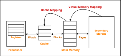
Fig 12 – Mapping process
Now, before proceeding further, it is important to note the following points-
|
Cache Mapping Techniques-
Cache mapping is performed using the following three different techniques-

In direct mapping,
Cache line number = ( Main Memory Block Address ) Modulo (Number of lines in Cache) |
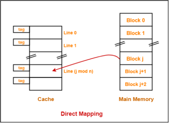
Fig 13 – Direct mapping
The need for a Replacement Algorithm-
In direct mapping,
In direct mapping, the physical address is divided as-
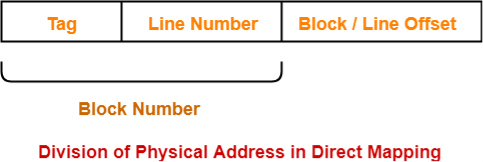
Fig 14 – Physical address
In fully associative mapping,
Consider the following scenario-
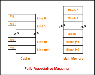
Fig 15 – Fully associative mapping
Here,
The need for a Replacement Algorithm-
In fully associative mapping,
Division of Physical Address-
In fully associative mapping, the physical address is divided as-

Fig 16 – Physical address
3. K-way Set Associative Mapping-
In k-way set associative mapping,
Cache set number = ( Main Memory Block Address ) Modulo (Number of sets in Cache) |
Example-
Consider the following example of 2-way set associative mapping-
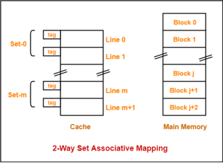
Fig 17 – 2-way set associative mapping
Here,
The need for a Replacement Algorithm-
In set associative mapping, the physical address is divided as-

Fig 18 – Physical address
1-way Set Associative Mapping ≡ Direct Mapping |
Key takeaway
OR
In an operating system that uses paging for memory management, a page replacement algorithm is needed to decide which page needs to be replaced when a new page comes in.
Page Fault – A page fault happens when a running program accesses a memory page that is mapped into the virtual address space but not loaded in physical memory.
Since actual physical memory is much smaller than virtual memory, page faults happen. In case of a page fault, Operating System might have to replace one of the existing pages with the newly needed page. Different page replacement algorithms suggest different ways to decide which page to replace. The target for all algorithms is to reduce the number of page faults.
Page Replacement Algorithms :
This is the simplest page replacement algorithm. In this algorithm, the operating system keeps track of all pages in the memory in a queue, the oldest page is in the front of the queue. When a page needs to be replaced page in the front of the queue is selected for removal.
Example-1Consider page reference string 1, 3, 0, 3, 5, 6 with 3 page frames.Find several page faults.
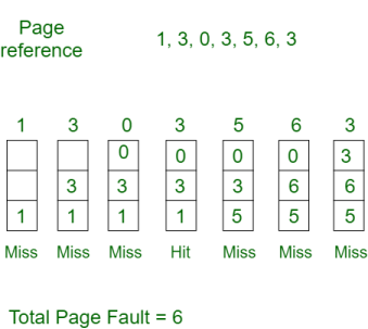
Initially, all slots are empty, so when 1, 3, 0 came they are allocated to the empty slots —> 3 Page Faults.
when 3 comes, it is already in memory so —> 0 Page Faults.
Then 5 comes, it is not available in memory so it replaces the oldest page slot i.e 1. —>1 Page Fault.
6 comes, it is also not available in memory so it replaces the oldest page slot i.e 3 —>1 Page Fault.
Finally, when 3 come it is not available so it replaces 0 1 page fault
Belady’s anomaly – Belady’s anomaly proves that it is possible to have more page faults when increasing the number of page frames while using the First in First Out (FIFO) page replacement algorithm. For example, if we consider reference string 3, 2, 1, 0, 3, 2, 4, 3, 2, 1, 0, 4, and 3 slots, we get 9 total page faults, but if we increase slots to 4, we get 10-page faults.
In this algorithm, pages are replaced which would not be used for the longest duration of time in the future.
Example-2:Consider the page references 7, 0, 1, 2, 0, 3, 0, 4, 2, 3, 0, 3, 2, with 4 page frame. Find number of page fault.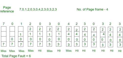
Initially, all slots are empty, so when 7 0 1 2 are allocated to the empty slots —> 4 Page faults
0 is already there so —> 0 Page fault.
when 3 came it will take the place of 7 because it is not used for the longest duration of time in the future.—>1 Page fault.
0 is already there so —> 0 Page fault.
4 will takes place of 1 —> 1 Page Fault.
Now for the further page reference string —> 0 Page fault because they are already available in the memory.
Optimal page replacement is perfect, but not possible in practice as the operating system cannot know future requests. The use of Optimal Page replacement is to set up a benchmark so that other replacement algorithms can be analyzed against it.
In this algorithm, the page will be replaced which is the least recently used.
Example-3Consider the page reference string 7, 0, 1, 2, 0, 3, 0, 4, 2, 3, 0, 3, 2 with 4 page frames.Find number of page faults.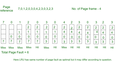
Initially, all slots are empty, so when 7 0 1 2 are allocated to the empty slots —> 4 Page faults
0 is already their so —> 0 Page fault.
when 3 came it will take the place of 7 because it is least recently used —>1 Page fault
0 is already in memory so —> 0 Page fault.
4 will takes place of 1 —> 1 Page Fault
Now for the further page reference string —> 0 Page fault because they are already available in the memory.
Key takeaway
A page fault happens when a running program accesses a memory page that is mapped into the virtual address space but not loaded in physical memory.
Since actual physical memory is much smaller than virtual memory, page faults happen. In case of a page fault, Operating System might have to replace one of the existing pages with the newly needed page. Different page replacement algorithms suggest different ways to decide which page to replace. The target for all algorithms is to reduce the number of page faults.
Normally we can perform both read operation and write operation on the cache memory.
Now when we perform a read operation on cache memory then it does not change the content of the memory. But as it is obvious that any write operation performed on the cache changes the content of the memory. Thus it is important to perform any write on cache very carefully.
To make sure write operation is performed carefully, we can adopt two cache write methods:
Let's learn about the above two cache write methods in computer architecture.
The write-through policy is the most commonly used methods of writing into the cache memory.
In the write-through method when the cache memory is updated simultaneously the main memory is also updated. Thus at any given time, the main memory contains the same data which is available in the cache memory.
It is to be noted that, the write-through technique is a slow process as every time it needs to access the main memory.
The write-back policy can also be used for cache writing.
During a write operation, only the cache location is updated while following the write-back method. When an update in cache occurs then the updated location is marked by a flag. The flag is known as modified or dirty bit.
When the word is replaced from the cache, it is written into the main memory if its flag bit is set. The logic behind this technique is based on the fact that during a cache write operation, the word present in the cache may be accessed several times (temporal locality of reference). This method helps reduce the number of references to the main memory.
The only limitation to the write-back technique is that inconsistency may occur while adopting this technique due to two different copies of the same data, one in the cache and the other in main memory.
Key takeaway
The write-through policy is the most commonly used methods of writing into the cache memory.
In the write-through method when the cache memory is updated simultaneously the main memory is also updated. Thus at any given time, the main memory contains the same data which is available in the cache memory.
The write-back policy can also be used for cache writing.
During a write operation, only the cache location is updated while following the write-back method. When an update in cache occurs then the updated location is marked by a flag. The flag is known as modified or dirty bit.
References:
1. “Computer Organization and Design: The Hardware/Software Interface”, 5th Edition by David A. Patterson and John L. Hennessy, Elsevier.
2. “Computer Organization and Embedded Systems”, 6th Edition by Carl Hamacher, McGraw Hill Higher Education.
Suggested reference books:
1. “Computer Architecture and Organization”, 3rd Edition by John P. Hayes, WCB/McGraw-Hill
2. “Computer Organization and Architecture: Designing for Performance”, 10th Edition by William Stallings, Pearson Education.
3. “Computer System Design and Architecture”, 2nd Edition by Vincent P. Heuring and Harry F. Jordan, Pearson Education.