Unit - 3
Frequency Compensation & Nonlinearity
Operational Amplifiers or Op-Amps are considered as the workhorse of Analog Electronic Designs. Back from the Analog computers era, Op-Amps have been used for mathematical operations with analog voltages hence the name operational amplifier. Till date Op-Amps are extensively used for voltage comparison, differentiation, integration, summation and many other things. Needless to say, the Operational Amplifier circuits are very easy to implement for different purposes but it has few limitations that often leads to complexity.
The major challenge is to improve the stability of an op-amp in a wide bandwidth of applications. The solution is to compensate the amplifier in terms of frequency response, by using a frequency compensation circuit across the operational amplifier. The stability of an amplifier is highly dependent on different parameters. In this article let’s understand the importance of Frequency Compensation and how to use it in your designs.
An amplifier can be configured as an open-loop configuration or a closed-loop configuration. In an open-loop configuration, there are no feedback circuits are associated with it. But in a closed-loop configuration, the amplifier needs feedback to work properly. The operational can have negative feedback or positive feedback. If the feedback network analog across the op-amp’s positive terminal, it is called positive feedback. Otherwise, negative feedback amplifiers have the feedback circuitry connected across negative terminal.
Need of Frequency Compensation
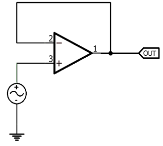
Fig 1 Non-Inverting Op-Amp
It is a simple negative feedback non-inverting Op-Amp circuit. The circuit is connected as a unity-gain follower configuration. As we all know, amplifiers have very high input impedance across the input and could provide a reasonable amount of current across the output. Therefore, operational amplifiers can be driven using low signals to drive loads of higher current.
The above circuit is good enough to drive pure resistive loads (ideal resistive load) but if we connect a capacitive load across the output, the op-amp will become unstable and based on the value of load capacitance at worst case the op-amp might even start to oscillate.
There are different types of frequency compensation techniques used in electronics. However, all techniques are categorized into two basic types of compensation technique. The first one is external compensation across the op-amp and the second one is the internal compensation technique.
The Solution is to provide frequency compensation to the op-amp. This is a useful technique to overcome the instability of the op-amp as well as improve the step response of the circuit.
Types of Op-Amp Frequency Compensation
There are different types of frequency compensation techniques used in electronics. However, all techniques are categorized into two basic types of compensation technique. The first one is external compensation across the op-amp and the second one is the internal compensation technique.
External Frequency Compensation in Op Amp
External compensation techniques vary depending on the application, type of amplifier used and many other things. The easiest way is to use out-of loop compensation technique or in-loop compensation technique.
Out of the loop compensation technique uses a simple resistor to isolate the capacitive load with the op-amp, lowering the capacitive loading of the op-amp. The resistor typically varies from 10-50 Ohms but the increase in isolated resistor effects the op-amp bandwidth. The bandwidth of the op-amp drastically reduced to a very low value. One of the popular ways of out of the loop frequency compensation techniques is to use Dominant pole compensation technique.
Dominant pole Compensation
This technique uses a simple RC network connected across the output of the operational amplifier circuit. A sample dominant pole compensation circuit is shown below.
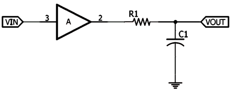
Fig 2 Dominant Pole Compensation
This works great to overcome the instability issue. The RC network creates a pole at unity or 0dB gain that dominates or cancels out other high-frequency poles effect. The transfer function of the dominant pole configuration is –

Where, A(s)is the uncompensated transfer function, A is the open-loop gain, ώ1, ώ2, and ώ3 are the frequencies where the gain roll-off at -20dB, -40dB, -60dB respectively. The Bode plot below shows what happens if the dominant pole compensation technique is added across the op-amp output, where fd is the dominant pole frequency.
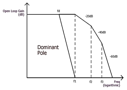
Fig 3 Dominant Pole Frequency
Pole Zero compensation:
Consider an op-amp with 3 break frequencies. Its loop gain be A.

Here the transfer function A is modified by adding a pole and zero with the help of compensating network. The zero added is at HF while the pole is at LF. Such a network is shown in figure
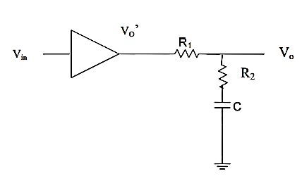
Fig 4 Pole Zero Compensation
Let A1 be the transfer function of the compensating network = Vo / Vo’
Let Z1=R1 & Z2 = R2-jXC2
By Voltage Divider rule,

On simplification,

On Simplification

Now let


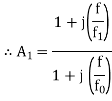
The values of Resistors and Capacitors are so selected that the break frequency for zero matches with the first corner frequency f1 of the uncompensated system while the pole of the compensating network at fo passes through 0 dB at the second corner frequency f2 of the uncompensated system. The loop gain becomes A’ = AA1.
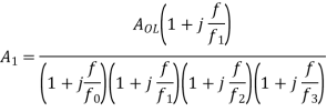
Where 0<f0<f1<f2. The, first corner frequency is now fo, and the gain starts rolling off at -20 dB / decade at fo. At f = f1, there is pole zero cancellation and rolling rate continues as -20 dB / decade. The values of Resistors and Capacitors are so selected that plot passes through 0 dB at f2. The response is shown in figure
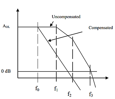
Fig 5 Pole Zero Compensation Response
As compared to the dominant pole compensation there is an improvement in bandwidth.
Internal Compensation Techniques
In recently developed op-amps like IC741, the compensation is built internally. A capacitor ranging from 10-30pF is fabricated between input and output stage to achieve the required compensation. This type of compensation is called Miller effect compensation. The demerit of dominant pole compensation techniques is overcome in this type. Here the capacitor is connected in the feedback path of the Darlington pair used in the output stage of the op-amp. These op-amps have single break frequency and are stable in nature. Some internally compensated op-amps are µA741, LM 107, LM 741, LM 112 and MC 1858.
Key takeaway
For Dominant pole compensation
Merits:
1) Excellent noise immunity system as the bandwidth is small.
2) By adjusting fd, adequate phase margin and stability of the system is assured.
Demerits:
The Bandwidth is drastically reduced for a compensated system.
Miller Compensation Technique- Use of a capacitor feeding back around a high-gain, inverting stage
- Miller capacitor only.
- Miller capacitor with an unity-gain buffer to block the forward path through the compensation capacitor. Can eliminate the RHP zero.
- Miller with a nulling resistor. Similar to Miller but with an added series resistance to gain control over the RHP zero.
Miller Compensation of the Two-Stage Op Amp
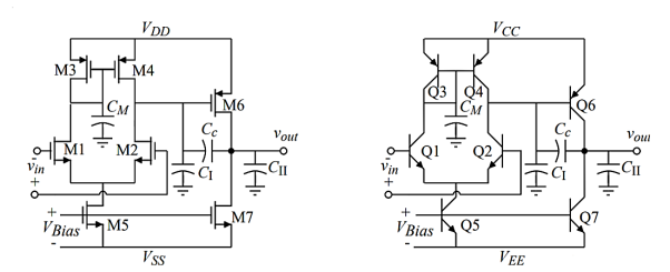
Fig 6 Miller Compensation
The various capacitors are
Cc = accomplishes the Miller compensation
CM = capacitance associated with the first-stage mirror (mirror pole)
CI = output capacitance to ground of the first-stage
CII = output capacitance to ground of the second-stage
Compensated Two-Stage, Small-Signal Frequency Response Model Simplified
Use the CMOS op amp to illustrate:
1.) Assume that gm3 >> gds3 + gds1
2.) Assume that gm3/CM >> GB
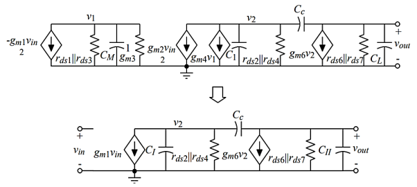
Fig 7 Small Signal Model
Same circuit holds for the BJT op amp with different component relationships.
General Two-Stage Frequency Response Analysis

Where:


The Nodal Equations are given by

And

Solving using Cramer’s Rule


Where

In General

 if
if


Key takeaway
Summary of Results for Miller Compensation of the Two-Stage Op Amp
There are three roots of importance:
1.) Right-half plane zero:

This root is very undesirable- it boosts the magnitude while decreasing the phase.
2.) Dominant left-half plane pole (the Miller pole):

This root accomplishes the desired compensation.
3.) Left-half plane output pole:

p2 must be ≥ unity-gain bandwidth or satisfactory phase margin will not be achieved.
Root locus plot of the Miller compensation:

Compensated Open-Loop Frequency Response of the Two-Stage Op Amp
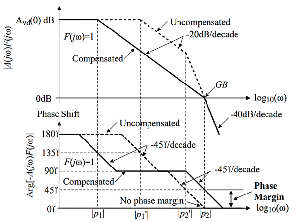
Note that the unity-gain bandwidth, GB, is

Remember that slew rate occurs when currents flowing in a capacitor become limited and is given as

Where vC is the voltage across the capacitor C.
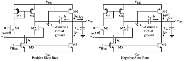
 because

Therefore, if CL is not too large and if I7 is significantly greater than I5, then the slew rate of the two-stage op amp should be, I5/Cc.
Key takeaway
• Op amps achieve accuracy by using negative feedback
• Compensation is required to insure, that the feedback loop is stable
• The degree of stability is measured by phase margin and is necessary to achieve small settling times
• A compensated op amp will have one dominant pole and all other poles will be greater than GB
• A two-stage op amp requires some form of Miller compensation
• A high output resistance op amp is compensated by the load capacitor
• Poles of a CMOS circuit are generally equal to the negative reciprocal of the product of the resistance to ground from a node times the sum of the capacitances connected to that node.
• The slew rate of the two-stage op amp is equal to the input differential stage current sink/source divided by the Miller capacitor
Most typical applications require op amp and its components to act linearly – I-V characteristics of passive devices such as resistors, capacitors should be described by linear equation ;Ohm’s LawͿ – For op amp, linear operation means input and output voltages are related by a constant proportionality (Av should be constant)
Some application requires op amps to behave in nonlinear manner (logarithmic and antilogarithmic amplifiers)
1) Gain Stabilization: The gain of a feedback system is almost entirely determined by the feedback path and not by the gain of the amplification path. This means that you can get predictable gains even when the gain of the amplification path is unknown or time-varying.
2) Distortion Reduction: High power amplifiers are often non-linear, e.g., their gain decreases at high signal amplitudes. Since the gain of a feedback system does not depend much on the gain of the amplification path, the non-linearity has little effect.
3) Interference Rejection: External disturbances have little effect on the output of a feedback system because the feedback adjusts to compensate for them
4) Increases Circuit Stability
The output of an amplifier without negative feedback is affected by the variations in the temperature, frequency, or amplitude of the signal which further changes the gain of the amplifier and as result, we get a distorted signal in the output. Hence, the negative feedback is applied so that the gain of the amplifier is stabilized.
5) Increases Input Impedance/Resistance
The use of negative feedback increases the input impedance or resistance of the amplifier.
Z’in = Zin. (1 + β. Av)
6) Reduces Noise Level
The negative feedback which we apply to the amplifiers is in the opposite phase to that of the applied input signal, hence it cancels out the noises which are introduced in the output signal by the amplifier circuit. As a result, we get the output signal with a reduced noise level.
7) Improves Frequency Response & Bandwidth
The negative feedback which we apply to the amplifiers is a resistive network hence the gain of the amplifier with negative feedback is independent of signal frequency. As a result, the gain becomes constant over a wide range of signal frequencies in this way the frequency response of the amplifier with negative feedback is improved.
f’cf = fcf . (1 + β .Av)
Here f’cf = resultant cut-off frequency with negative feedback
fcf = cut-off frequency without feedback
Key Takeaways
- Negative feedback amplifiers have an important role in reducing amplitude distortion, frequency distortion, and phase distortion.
- With feedback, the overall gain of the amplifier becomes

- The distortion in the feedback amplifier gets reduced by a factor of

Log Amplifier using diode
As the name says it is an amplifier which produces the output proportional to logarithmic of the applied input. The log amplifier using op-amp is shown below. The input is applied through the inverting end of op-amp. As the non-inverting end has voltage zero then by virtual ground concept the voltage at inverting terminal also becomes zero.
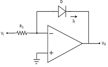
Fig 8 Log Amplifier
The equation for input voltage will be
 +If = 0
If = 
The current flowing through diode is given as

Here:
Is = Saturation Current
Vf = Voltage drops across diode in forward bias
VT = Thermal equivalent voltage
For feedback loop the KVL equation will be
0-Vf -V0 = 0
Vf = -V0
Substituting Vf in above equation of If

Equating both equations of If


Taking natural log of both sides we get


The above equations shows that the output is natural log of the applied input.
Op-amp transistor log amplifier
In this configuration a transistor is placed in the feedback path of an op-amp wired in inverting mode. Collector of the transistor is connected to the inverting input of the op-amp, emitter to output and base is grounded. The necessary condition for a log amp to work is that the input voltage must be always positive. Circuit diagram of an Op-amp-transistor log amplifier is shown below.
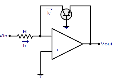
Fig 9 Log Amplifier using BJT
The base-emitter voltage of the transistor Vbe = -Vout ………(1)
We know that Ic = Iso (e(Vbe/Vt)-1) ………….(2)
Where Ic is the collector current of the transistor, Iso the saturation current, Vbe
The base emitter voltage and Vt the thermal voltage.
Equation (1) can be approximated as Ic = Iso e(Vbe/Vt) ………….(3)
i.e., Vbe = Vt In (Ic/Iso) …………….(4)
Since input pin of an ideal op-amp has infinite input impedance, the only path for the input current Ir is through the transistor and that means Ir = Ic.
Since the inverting input of the op-amp is virtually grounded
Ir = Vin/R
That means Ic = Vin/R ……………(5)
From equations (5), (4) and (1) it is clear that
Vout = -Vt ln (Vin/IsoR1)………….(6)
Antilog Amplifier using diode and Transistor
This device produces the output proportional to antilog of input. The inverting op-amp is used in this case as well. The figure below shows an antilog amplifier with its inverting terminal connected to the input end with diode and the non-inverting terminal is grounded.
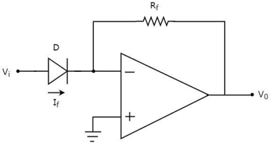
Fig 10 Antilog Amplifier using Diode
Applying KCL at input terminal we get


The current flowing through diode is given as

Substituting If in above voltage equation we get


At inverting terminal applying KVL we get


Substituting Vf in equation of V0 we get

The above equations shows that the output is natural antilog of the applied input.
Anti-Log Amplifier Using BJT
Basic Anti Log amplifier using transistor It is obtained by using a transistor as a diode in the input path of an op-amp as shown in the figure. The node B is at virtual ground, hence VB = 0. Thus, the collector and base are both at ground potential and VCB = 0. Hence the voltage across the transistor is VBE and we can write,

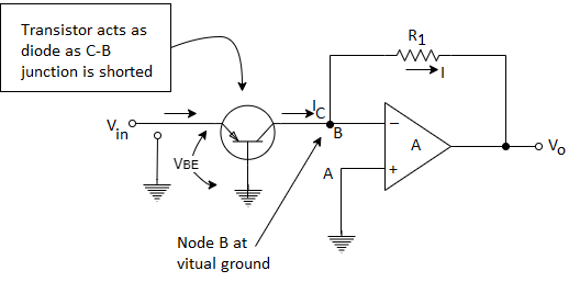
Fig 11 Antilog amplifier using Transistor
From the figure, VBE = Vin. Then

Now the current  and current I are same as op-amp input current is zero.


Let 

The output voltage is proportional to the exponential of Vin i.e., antilog of Vin. Thus, circuit works as basic antilog amplifier. In both the above circuits it can be seen that the terms I0, Is and VT are present in the output equation. All these are the function of temperature. Hence, a temperature changes, these parameters also change and causes serious errors at the output.
Key takeaways
For Log Amplifier


For Antilog Amplifier

For Log Amplifier the circuit has one problem. The emitter saturation current Is varying from transistor to transistor and with temperature. Thus, a stable reference voltage V ref cannot be obtained. This is eliminated by the circuit given below
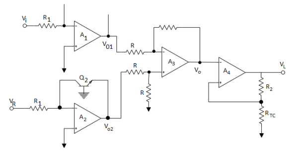
Fig 12 Log Amplifier with compensation of emitter saturation current
The input is applied to one log-amp, while a reference voltage is applied to one log-amp, while a reference voltage is applied to another log-amp. The two transistors are integrated close together in the same silicon wafer. This provides a close match of saturation currents and ensures good thermal tracking.
Assume IS1=IS2=IS
Thus, the reference level is now set with a single external voltage source. Its dependence on device and temperature has been removed. The voltage Vo is still dependent upon temperature and is directly proportional to T. This is compensated by the last op-amp stage A4 which provides a non-inverting gain of (1+R2/RTC). Temperature compensated output voltage VL

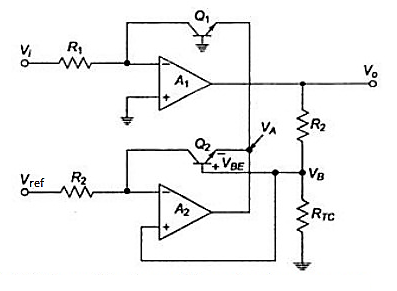
Fig 13 Logarithmic Amplifier using Two-Op-Amps
Where RTC is a temperature-sensitive resistance with a positive coefficient of temperature (sensor) so that the slope of the equation becomes constant as the temperature changes.
For Antilog Amplifiers temperature compensation is achieved by same technique.
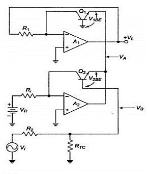
Fig 14 Antilog amplifier
 and
and  and
and


Therefore 
Rearranging we get


We know that
Therefore, 


Rectifier circuit gives average value of input signal; but in practice we need peak value of input signal. This is achieved by peak detector circuit. The following figure shows a simple peak detector circuit using diode and capacitor.
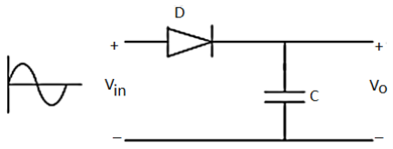
Fig 15 Peak detector
In the positive half cycle, diode D is forward biased and capacitor C starts charging. When input reaches its peak value, capacitor gets charged to positive peak value.
In negative half cycle, as input decreases, diode D is reversed biased and capacitor is isolated and holds the peak value of previous cycle. Hence called as peak detector.
But in practice, output is taken across some load RL, so when input voltage decreases capacitor discharges through load RL. To avoid this, select RL of very large value so that capacitor discharges very slowly hence almost hold the charge. Whatever charge it lost through RL is gets back in next half cycle.
Key takeaway
The diode D is acting as an instant switch, so supply gets loaded. To avoid the loading while charging capacitor, we use op-amp.
- The Sample and Hold circuit are an electronic circuit which creates the samples of voltage given to it as input, and after that, it holds these samples for the definite time. The time during which sample and hold circuit generates the sample of the input signal is called sampling time.
- Similarly, the time duration of the circuit during which it holds the sampled value is called holding time.
- Sampling time is generally between 1µs to 14 µs while the holding time can assume any value as required in the application.
- It will not be wrong to say that capacitor is the heart of sample and hold circuit.
- This is because the capacitor present in it charges to its peak value when the switch is opened, i.e., during sampling and holds the sampled voltage when the switch is closed.
Need for Sample and Hold Circuits
If the input analog voltage of an ADC changes more than ±1/2 LSB, then there is a severe chance that the output digital value is an error. For the ADC to produce accurate results, the input analog voltage should be held constant for the duration of the conversion.
It is based on a sampling command and holds the output value at its output until the next sampling command is arrived.
The following image shows the input and output of a typical Sample and Hold Circuit.
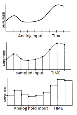
Fig 16 Input and output of S/H circuit
This sample and hold circuit consist of two basic components:
- Analog Switch
- Holding Capacitor
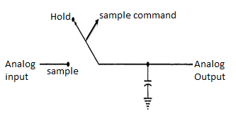
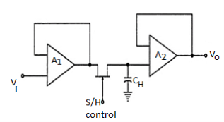
Fig 17 Open loop s/h circuit
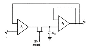
Fig 18 Closed loop s/h circuit
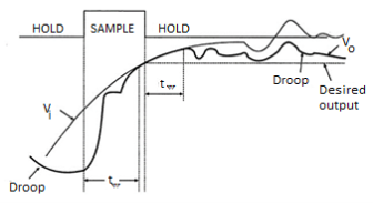
Fig 19 S/H characteristics
Acquisition Time (tac)
The time required for the charge in the holding capacitor to rise up to a level that is close to the input voltage during the sampling is called acquisition time. It is affected by three factors:
- The RC Time Constant
- The Slew-Rate of the Op-Amp
- The maximum output current of the Op-Amp
Aperture Time (tap)
The time delay between the initiation of VO tracking the Vi and the initiation of the hold command is called the Aperture Time. This delay is usually due to the propagation delays through the driver and the switch circuits.
For a precise timing operation, the hold command must be initiated in advance by an amount of aperture time.
Aperture Uncertainty (∆ tap)
The Aperture time will not be the same for all the sample and will vary from sample to sample. This uncertainty is called Aperture Uncertainty. This will severely affect the advancing of the hold command.
Hold Mode Settling Time (ts)
The hold mode settling time is the time taken by the output VO to settle within the specified error band (usually 1%, 0.1% or 0.01%) after the application of hold command.
Hold Step
During the switching from sample mode to hold mode, there might an unwanted transfer of charge between the switch and the holding capacitor (mainly due to the parasitic capacitances). This will affect the capacitor voltage as well as the output voltage. This change in the output voltage from the desired voltage is called Hold Step.
Feedthrough
Again, the parasitic capacitances in the switch may cause AC coupling between VO and Vi in hold mode. As a result, the output voltage may vary with changes in the input voltage and this is referred to as feedthrough.
Droop
Voltage Droop is a phenomenon where the voltage across the holding capacitor drops down due to leakage currents.
Advantages
- The main and important advantage of a typical SH Circuit is to aid an Analog to Digital Conversion process by holding the sampled analog input voltage.
- In multichannel ADCs, where synchronization between different channels is important, an SH circuit can help by sampling analog signals from all the channels at the same time.
- In multiplexed circuits, the crosstalk can be reduced with an SH circuit.
Key takeaways
They are used in
- Analog to Digital Converter Circuits (ADC)
- Digital Interface Circuits
- Operational Amplifiers
- Analog De-multiplexers
- Data distribution systems
- Storage of outputs of multiplexers
- Pulse Modulation Systems
Comparator
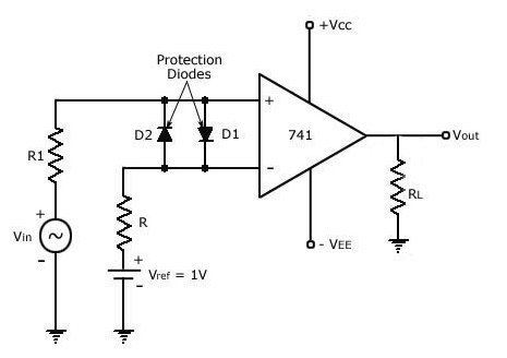
Fig 20 Comparator
- A reference voltage Vref of 1V is applied to the inverting terminal of op-amp.
- A time varying voltage Vin is applied to the non-inverting terminal of op-amp.
- Diode D1 and D2 are used to protect the op-amp from damage from excess amount of input voltage Vin.
- They are known as clamp diodes as they clamp the difference input voltage to +0.7V to -0.7V.
- Hence, the above circuit is called as non-inverting Comparator.
Characteristics of comparator
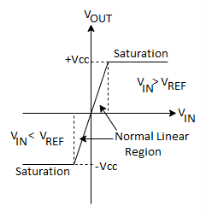
Fig 21 Voltage levels for comparator
- When Vin <Vref, then output Vo = -Vsat (≈ -Vee) because the voltage at negative input is higher than that of positive input.
- When Vin >Vref, then output Vo = +Vsat (≈ +Vee) as the positive input becomes positive with respect to the negative input.
- When Vin ≈ Vref, then Vo changes from one Vsat level to another.
- Therefore, the comparator is a type of analog to digital converter.
- It is also known as Voltage Level Detector because for a particular value of Vref, the voltage level of Vin can be detected.
Zero Crossing Detector
An op-amp detector that has the ability to detect the change from positive to negative or negative to a positive level of a sinusoidal waveform is known as a zero- crossing detector.
It is also known to be a square wave generator as the applied input signal is converted into a square wave by the zero -crossing detector.
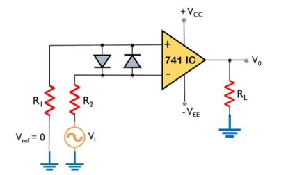
Fig 22 Zero crossing Detector
Here, the input signal Vi is provided to the inverting terminal of the op-amp while the non-inverting terminal is grounded by making use of two resistors R1 and R2.
It detects the point where the input signal crosses zero of the reference voltage level. For every crossing, the saturation level of the output signal changes from one to another.
The reference level is set at 0 and applied at the non-inverting terminal of the op-amp. The sine wave applied at the inverting terminal of the op-amp is compared with the reference level each time the phase of the wave changes either from positive to negative or negative to positive.
Firstly, when positive half of the sinusoidal signal appears at the input. Then the op-amp comparator compares the reference voltage level with the peak level of the applied signal.
Vo = Vref – Vi ---------------------------------------(1)
And we know the reference level is 0, thus
Vo = 0 – (+ Vsat) ----------------------------------------(2)
Therefore, Vo = - Vsat ---------------------------------(3)
During the negative half of the signal, thus the peak will have a negative polarity.
Again
Vo = Vref – Vi ---------------------------------------------(4)
Thus,
Vo = 0 - (- Vsat) --------------------------------------------------(5)
So, we get
Vo = + Vsat ---------------------------------------------(6)
In this way, the zero -crossing detector detects the change in the level of the applied signal.
Zero crossing detector is also known to be a square wave generator. As the output of the window comparator is nothing but a square wave.
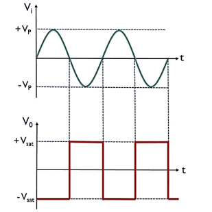
Fig 23 Input and output of zero crossing detector
V0 for the positive half of the applied signal is – Vsat,
This is the reason why we have achieved negative half of the square wave at the output when positive half of the sinusoidal signal is applied. While V0 for the negative half of the sinusoidal signal is + Vsat,
Applications:
- Phase Locked Loop
- Frequency counters and phase meters
Key takeaways
- An op-amp detector that has the ability to detect the change from positive to negative or negative to a positive level of a sinusoidal waveform is known as a zero- crossing detector.
- When Vin <Vref, then output Vo = -Vsat (≈ -Vee) because the voltage at negative input is higher than that of positive input.
- When Vin >Vref, then output Vo = +Vsat (≈ +Vee) as the positive input becomes positive with respect to the negative input.
The astable multivibrator shown in the figure below [Ref.1] can be used to generate square wave oscillations. The diode is connected across RB and the diode and capacitor are charged through RA to a voltage of 2/3 of VCC. The capacitor discharges through RB and Q1. The discharging of capacitor when reaches 1/3VCC the discharging stops.
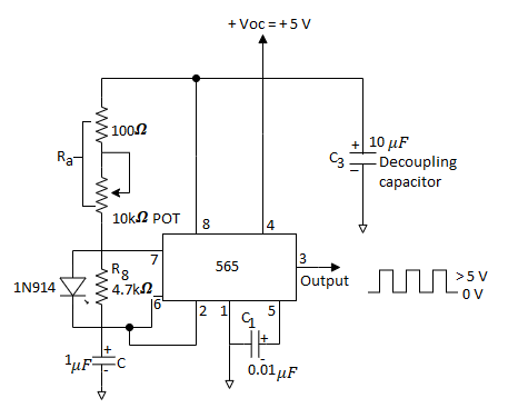
Fig 24 Astable multivibrator as square wave oscillator
Monostable Multivibrator
It also called one shot, operates by charging a timing capacitor with a current set by external resistance. When the one shot is triggered, the charging network cycles only once during the timing interval. The total timing interval includes the recovery time needed for the capacitor to charge up to the threshold level.
When Vcc high is applied to the trigger input, the trigger comparator output is low, the flip flop output is high, the transistor is on, the timing capacitor is discharged to ground potential. The output of the 555 circuit is low.
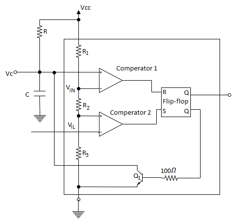
Fig 25 Monostable multivibrator
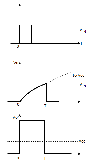
Fig 26 Output waveform
When negative voltage is applied to the trigger input, output of trigger comparator goes high. When trigger pulse drops below 1/3 Vcc output of flip flop goes low, output of 555 circuit goes high and the transistor turns off
Key takeaways
It also called one shot, operates by charging a timing capacitor with a current set by external resistance.
The op-amp IC used in this stage is also uA741 (IC2). Resistor R5 in conjunction with R4 sets the gain of the integrator and resistor R5 in conjunction with C2 sets the bandwidth. The square wave signal is applied to the inverting input of the op-amp through the input resistor R4. The op-amp integrator part of the circuit is shown in the figure below.
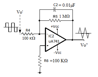
Fig 27 Triangular waveform generator
After this initial “kick” the capacitor starts charging and it creates an opposition to the input current flowing through the input resistor R4. The negative feedback compels the op-amp to produce a voltage at its out so that it maintains the virtual ground at the inverting input.
Since the capacitor is charging its impedance Xc keeps increasing and the gain Xc2/R4 also keeps increasing. This results in a ramp at the output of the op-amp that increases in a rate proportional to the RC time constant (T=R4C2) and this ramp increases in amplitude until the capacitor is fully charged.
When the input to the integrator (square wave) falls to the negative peak the capacitor quickly discharges through the input resistor R4 and starts charging in the opposite polarity.
Now the conditions are reversed, and the output of the op-amp will be a ramp that is going to the negative side at a rate proportional to the R4R2 time constant. This cycle is repeated, and the result will be a triangular waveform at the output of the op-amp integrator.
Key takeaways
Since the capacitor is charging its impedance Xc keeps increasing and the gain Xc2/R4 also keeps increasing. This results in a ramp at the output of the op-amp that increases in a rate proportional to the RC time constant (T=R4C2) and this ramp increases in amplitude until the capacitor is fully charged.
A multiple produces an output V0 which is proportional to the product of two inputs Vx and Vy. V0 = KVxVy where K is the scaling factor = (1/10) V-1. There are various methods available for performing analog multiplication. Four of such techniques, namely,
1. Logarithmic summing technique
2. Pulse height/width modulation Technique
3. Variable trans conductance Technique
4. Multiplication using Gilbert cell and
5. Multiplication using variable trans conductance technique. An actual multiplier has its output voltage V0 defined by

Where φx and φy are the offsets associated with signals Vx and Vy, ε is the error signal associated with K and φ0 is the offset voltage of the multiplier output. Terminologies associated voltage of the multiplier characteristics:
Accuracy: This specifies the derivation of the actual output from the ideal output, for any combination of X and Y inputs falling within the permissible operating range of the multiplier.
Linearity: This defines the accuracy of the multiplier. The Linearity Error can be defined as the maximum absolute derivation of the error surface. This linearity error imposes a lower limit on the multiplier accuracy.
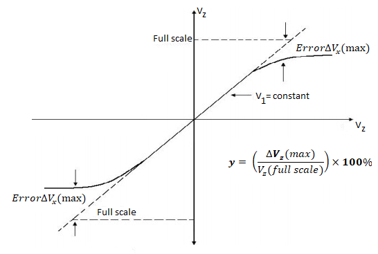
The figure shows the response of the output as a function of one input voltage Vx when the other Vy is assumed constant. It represents the maximum percentage derivation from the ideal straight-line output. An error surface is formed by plotting the output for different combinations of X and Y inputs.
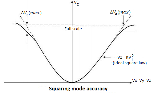
Square law accuracy: The Square – law curve is obtained with the X and Y inputs connected together and applied with the same input signal. The maximum derivation of the output voltage from an ideal square –law curve expresses the squaring mode accuracy
Bandwidth: The Bandwidth indicates the operating capability of an analog multiplier at higher frequency values. Small signal 3 dB bandwidth defines the frequency f0 at which the output reduces by 3dB from its low frequency value for a constant input voltage. This is identified individually for the X and Y input channels normally. The transconductance bandwidth represents the frequency at which the transconductance of the multiplier drops by 3dB of its low frequency value. This characteristic defines the application frequency ranges when used for phase detection or AM detection.
Quadrant: The quadrant defines the applicability of the circuit for bipolar signals at its inputs. First – quadrant device accepts only positive input signals, the two-quadrant device accepts one bipolar signal and one unipolar signal and the four-quadrant device accepts two bipolar signals. ✓ Logarithmic summing Technique: This technique uses the relationship
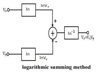
LnVx + lnVy =ln(VxVy)
As shown in figure the input voltages Vx and Vy are converted to their logarithmic equivalent, which are then added together by a summer. An antilogarithmic converter produces the output voltage of the summer. The output is given by,
Vz = ln-1 (ln(Vx Vy )) = Vx Vy .
The relationship between I0 and VBE of the transistor is given by IC = I0 e(VBE /VT ) .It is found that the transistor follows the relationship very accurately in the range of 10nA to 100mA. Logarithmic multiplier has low accuracy and high temperature instability. This method is applicable only to positive values of Vx and Vy.
References:
1. Gayakwad: Op-Amps and Linear Integrated Circuits, 4th Edition Prentice Hall of India, 2002.
2. Franco, Analog Circuit Design: Discrete & Integrated, TMH, 1st Edition.
3. Salivahnan, Electronics Devices and Circuits, TMH, 3rd Edition, 2015
4. Millman and Halkias: Integrated Electronics, TMH, 2nd Edition, 2010