Unit - 1
INTRODUCTION TO MOS TRANSISTOR
The most basic element in the design of large- scale integrated circuit is the transistor. The type of transistor available is the Metal-Oxide-Semiconductor Field Effect Transistor (MOSFET). These transistors form as a sandwich'' consisting of semiconductor layer, a slice or wafer, which from a single crystal of silicon; a layer of silicon dioxide and a layer of metal. These layers are patterned in a manner which permits transistors to be formed in the semiconductor material the substrate'.
The diagram showing a typical MOSFET
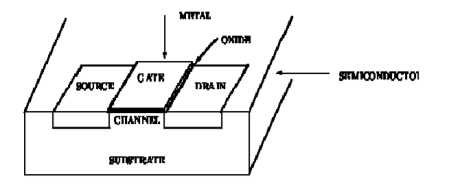
Figure 1. MOS Transistor
The transistor consists of three regions, labelled as the source'', gate'' and the drain''. The area labelled as the gate region forms a sandwich consisting of the underlying substrate material. The electrical charge or current can flow from the source to the drain depending on the charge applied to the gate region. The semiconductor material in the source and drain region are doped'' with a different type of material than in the region under the gate, so NPN or PNP type structure exists between the source and drain region of a MOSFET.
In Figure 2 (a), the source and drain regions are doped with N type material and the substrate doped with P type material. Such a transistor is called an N channel MOSFET.
If they were doped with P type material, and the substrate doped with N type material as in Figure 2 (b), the device would be called a P channel MOSFET.
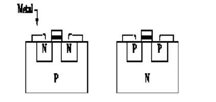
Figure 2(a) N channel MOSFET (b) P channel MOSFET
Key takeaways:
MOS-technology is the dominating LSI-technology. MOS-transistors have been scaled from long to short channels.
The MOSFET (metal-oxide-semiconductor field-effect transistor) are of two types: PMOS (p-type MOS) and NMOS (n-type MOS).
A new type of MOSFET logic is made combining both the PMOS and NMOS processes and is called as complementary MOS (CMOS).
CMOS stands for “Complementary Metal Oxide Semiconductor”.
It is one of the most popular technology in the chip design industry and is used today to form integrated circuits for various applications.
Computer memories, CPUs and cell phones make use of this technology due to various advantages. This technology uses both P and N channel semiconductor devices.
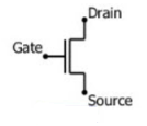
NMOS
NMOS is built on a p-type substrate with n-type source and drain diffused on it. Here, the majority carriers are electrons. When a high voltage is applied to the gate, the NMOS conducts and when low voltage is applied to the gate, it does not conduct. NMOS is faster than PMOS, as the carriers are electrons that travel twice as fast as the holes.
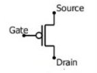
PMOS
P-MOS consists of P-type Source and Drain diffused on an N-type substrate. Here, majority carriers are holes. When a high voltage is applied to the gate, the PMOS does not conduct and when a low voltage is applied, it conducts. These devices are more immune to noise than NMOS devices.
CMOS Applications
- Computer memories, CPUs
- Microprocessor designs
- Flash memory chip designing
- Used to design application specific integrated circuits (ASICs)
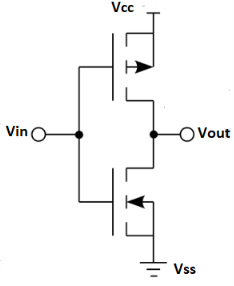
Fig 3 CMOS
The inverter circuit as shown in the figure above. It consists of PMOS and NMOS FET. The input A serves as the gate voltage for both transistors.
The NMOS transistor has an input from Vss (ground) and PMOS transistor has an input from Vdd. The terminal Y is output. When a high voltage (~ Vdd) is given at input terminal (A) of the inverter, the PMOS becomes open circuit and NMOS switched OFF so the output will be pulled down to Vss.
When a low-level voltage (<Vdd, ~0v) applied to the inverter, the NMOS switched OFF and PMOS switched ON. So, the output becomes Vdd or the circuit is pulled up to Vdd.
INPUT | LOGIC INPUT | OUTPUT | LOGIC OUTPUT |
0 V | 0 | Vdd | 1 |
Vdd | 1 | 0 v | 0 |
Key takeaway
CMOS stands for “Complementary Metal Oxide Semiconductor”.
It is one of the most popular technology in the chip design industry and is used today to form integrated circuits for various applications.
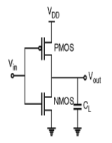
Fig 4: CMOS inverter
- It consists of PMOS and NMOS FET.
- The input A serves as the gate voltage for both transistors.
- The NMOS transistor has an input from Vss (ground) and PMOS transistor has an input from Vdd. The terminal Y is output.
- When a high voltage (~ Vdd) is given at input terminal (A) of the inverter, the PMOS becomes open circuit and NMOS switched OFF so the output will be pulled down to Vss.
- The truth table of inverter is:
A | Y = A’ |
0 | 1 |
1 | 0 |

Fig.5: NOT gate (ref. 1)
Key takeaway
It inverts the input applied to it.
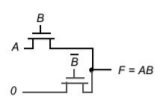
Fig 6 Pass Transistor
A popular and widely-used alternative to complementary CMOS is pass-transistor logic, which attempts to reduce the number of transistors required to implement logic by allowing the primary inputs to drive gate terminals as well as source/drain terminals. This is in contrast to logic families that we have studied so far, which only allow primary inputs to drive the gate terminals of MOSFETS. Pass-transistor gates cannot be cascaded by connecting the output of a pass gate to the gate input of another pass transistor.

Fig 7 Pass transistor output (Drain/Source) terminal should not drive other gate terminals to avoid multiple threshold drops.
Key takeaway
Pass-transistor gates cannot be cascaded by connecting the output of a pass gate to the gate input of another pass transistor.
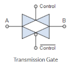
When PMOS and NMOS devices together are connected in parallel then a basic bilateral CMOS switch is created and is known as a “Transmission Gate”. Here, the transmission gate is symmetrical, or bilateral, that is, the input and output are interchangeable. This bilateral operation is shown in the transmission gate symbol below which shows two superimposed triangles pointing in opposite directions to indicate the two signal directions.
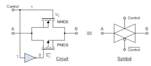
Fig 8 Transmission gate
Both MOS transistors are connected back-to-back in parallel with an inverter used between the gate of the NMOS and PMOS to provide the two complementary control voltages. When the input control signal, VC is LOW, both the NMOS and PMOS transistors are cut-off and the switch is open. When VC is high, both devices are biased into conduction and the switch is closed.
When VC = 1, the transmission gate acts as a “closed” switch,
When VC = 0, it operates as a voltage-controlled switch.
The bubble of the symbol indicating the gate of the PMOS FET.
Symbol
Truth Table
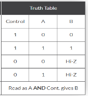
Boolean Expression B = A. Control
Key takeaway
When PMOS and NMOS devices together are connected in parallel then a basic bilateral CMOS switch is created and is known as a “Transmission Gate”.
The design rules primary address two issues:
1. The geometrical reproduction of features that can be reproduced by the mask making and lithographical process, and
2. The interaction between different layers.
There are primarily two approaches in describing the design rules.
1. Linear scaling is possible only over a limited range of dimensions.
2. Scalable design rules are conservative. This, results in over dimensioned and less dense design.
3. This rule is not used in real life.
1. Scalable Design Rules (e.g., SCMOS, λ-based design rules):
In this approach, all rules are defined in terms of a single parameter λ. The rules are so chosen that a design can be easily ported over a cross section of industrial process, making the layout portable. Scaling can be easily done by simply changing the value of. The key disadvantages of this approach are:
2. Absolute Design Rules (e.g., μ-based design rules): In this approach, the design rules are expressed in absolute dimensions (e.g., 0.75μm) and therefore can exploit the features of a given process to a maximum degree. Here, scaling and porting is more demanding, and has to be performed either manually or using CAD tools. Also, these rules tend to be more complex especially for deep submicron.
The fundamental unity in the definition of a set of design rules is the minimum line width. It stands for the minimum mask dimension that can be safely transferred to the semiconductor material. Even, for the same minimum dimension, design rules tend to differ from company to company, and from process to process. Now, CAD tools allow designs to migrate between compatible processes.
Layer Representations
With increase of complexity in the CMOS processes, the visualization of all the mask levels that are used in the actual fabrication process becomes inhibited. The layer concept translates these masks to a set of conceptual layout levels that are easier to visualize by the circuit designer. From the designer's viewpoint, all CMOS designs have the following entities:
• Two different substrates and/or wells: which is p-type for NMOS and n-type for PMOS.
• Diffusion regions (p+ and n+): which defines the area where transistors can be formed. These regions are also called active areas. Diffusion of an inverse type is needed to implement contacts to the well or to substrate. These, are called select regions.
• Transistor gate electrodes: Polysilicon layer
• Metal interconnect layers
• Interlayer contacts and via layers. The layers for typical CMOS processes are represented in various figures in terms of:
• A color scheme (Mead-Conway colors).
• Other color schemes designed to differentiate CMOS structures.
• Varying stipple patterns
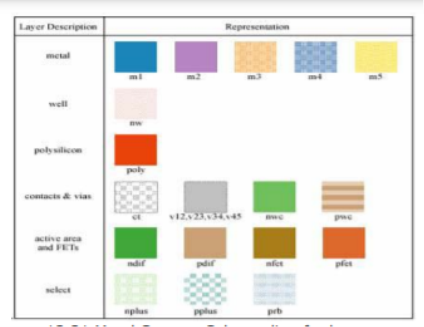
Fig 9 Mead Conway Colour coding for layers
Key takeaway
With increase of complexity in the CMOS processes, the visualization of all the mask levels that are used in the actual fabrication process becomes inhibited.
An example of layer representations for CMOS inverter using above design rules is shown below
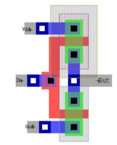
Fig 10 CMOS inverter Layout
Another popular method of symbolic design is "Sticks" layout. In this, the designer draws a freehand sketch of a layout, using coloured lines to represent the various process layers such as diffusion, metal and polysilicon. Where, polysilicon crosses diffusion, transistors are created and where metal wires join diffusion or polysilicon, contacts are formed. This notation indicates only the relative positioning of the various design components. The absolute coordinates of these elements are determined automatically by the editor using a compactor.
The compactor translates the design rules into a set of constraints on the component positions, and solve a constrained optimization problem that attempts to minimize the area or cost function. The advantage of this symbolic approach is that the designer does not have to worry about design rules, because the compactor ensures that the final layout is physically correct. The disadvantage of the symbolic approach is that the outcome of the compaction phase is often unpredictable. The resulting layout can be less dense than what is obtained with the manual approach. In addition, it does not show exact placement, transistor sizes, wire lengths, wire widths, tub boundaries.
For example, stick diagram for CMOS Inverter is shown below

Fig 11 Stick Diagram of CMOS inverter
Key takeaway
In this, the designer draws a freehand sketch of a layout, using coloured lines to represent the various process layers such as diffusion, metal and polysilicon.
In this section, the relation between IDS and VGS and is discussed. We assume that gate body voltage drop is more than threshold voltage VT, so that mobile electrons are created in the channel. This implies that the transistor is either in linear or saturation region. Here we will derive some simple I-V characteristics of MOSFET, assuming that the device essentially acts as a variable resistor between source and drain, and only drift ohmic current needs to be calculated. Also note that the MOSFET is basically a two-dimensional device.
The gate voltage produces a field in the vertical (x) direction, which induces charge in the silicon, including charge in the inversion layer. The voltage produces a field in the lateral (y) direction, and current flows (predominantly) in the y-direction. Strictly speaking, we must solve the 2-D Poisson and continuity equations to evaluate the I-V characteristics of the device. These are analytically intractable. We therefore resort to the gradual channel approximation described below. To find the current flowing in the MOS transistor, we need to know the charge in the inversion layer.
This charge, Qn(y) (per sq. Cm) is a function of position along the channel, since the potential varies going from source to drain. We assume that Qn(y) can be found at any point y by solving the Poisson equation only in the x direction, that is treating the gate-oxide-silicon system in the channel region very much like a MOS capacitor. This is equivalent to assuming that vertical electric field Ex is much larger than the horizontal electric field Ey, so that the solution of the 1-dimensional Poisson equation is adequate. This gradual channel approximation (the voltage varies only gradually along the channel) is quite valid for long channel MOSFETs since Ey is small. For Qn(y) using charge control relation at location y we have:
|Qn(y)| = Cox (VGS – VT – V(y)) VGS – V(y)>VT
Now we turn our attention to evaluate the resistance of the infinitesimal element of length dy along the channel. Assuming that only drift current is present and hence applying Ohm's law, we get
R =  = l/
= l/
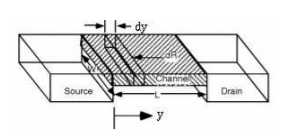
Fig 12 Cross Sectional view of channel
But I = dy,  =qn(x)
 and A=Wxi where xi is the inversion layer thickness.
DVy/IDS(y) = dy/
As  is varying along the traverse direction, we define
  av as
av as
 av =
av =
IDS(y)dy = |Qn(y)| WdV(y)
Now we can write
IDS L =  W
W 
IDS = 
IDS =  ]
]
The drain current first increases linearly with the applied drain-to-source voltage, but then reaches a maximum value. This occurs due to the formation of depletion region between pinch-off point and drain. This behaviour is known as drain saturation which is observed VGS-VT<VDS for as shown in figure below.
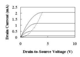
Fig 13 IDS-VDS graph
The saturation current IDSsat is given by equation
IDSSat = 
Key takeaway
The gate voltage produces a field in the vertical (x) direction, which induces charge in the silicon, including charge in the inversion layer. The voltage produces a field in the lateral (y) direction, and current flows (predominantly) in the y-direction.
The saturation current IDSsat is given by equation
IDSSat = 
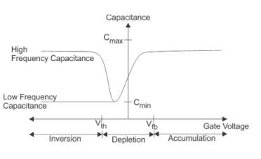
Fig:14 Capacitance vs. Gate Voltage (CV) diagram
The flat band voltage (Vfb) separates the Accumulation region from the Depletion region. The threshold voltage (Vth) separates the depletion region from the inversion region.
The I-V characteristics designed so far neglect many effects that are important in modern deep-submicron processes.
§ Velocity Saturation and Mobility Degradation
§ Channel length modulation
§ Sub threshold conduction
§ Tunneling
§ Junction leakage
§ Body effect
§ Temperature and Geometry dependence
The VTC is divided into five regions (1-5) for easy of understanding. The above shown curve is possible when both T1 and T2 are matched for optimum operation. Optimum operation is achieved when Vin = Vdd/2 we get Vout = Vdd/2. This can be achieved by adjusting width and length of both T1 and T2 as other parameters like mobility, oxide capacitance varies between different technologies.
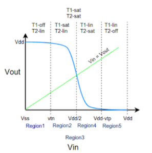
Fig 15 DC Transfer Characteristics
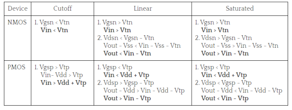
Region-1
In this, the input is in the range of (0, Vtn).
- NMOS is in cutoff as Vgs < Vtn
- PMOS is in linear as Vgsp < Vtp and Vdsp > Vgsp -Vtp.
- Zero current flows from supply voltage and the power dissipation is zero.
Region-2
Here, the input is in the range of (Vtn, Vdd/2).
- NMOS is in saturation as Vgs > Vtn and Vout >Vin – Vtn.
- PMOS is in linear region as Vdsp > Vgsp -Vtp.
- Since both the transistors are conducting some amount of current flows from supply in this region.
Region-3
Here the input voltage is Vdd/2. At this point the output voltage is Vdd/2. Here both the NMOS and PMOS are in saturation and the output drops drastically from Vdd to Vdd/2. At this point a large amount of current flows from the supply.
- NMOS is in saturation as Vgs > Vtn and Vout >Vin - Vtn.
- PMOS is in saturation as Vgsp < Vtp and Vdsp < Vgsp -Vtp.
- Large amount of current is drawn from supply and hence large power dissipation.
Region-4
In this region the input voltage is in the range of (Vdd/2, Vdd-Vtp). Here the PMOS remains in saturation as Vout < Vin - Vtp and Vgsp < Vtp. But the NMOS moves from saturation to linear region since the drain to source voltage now is less than Vgsn-Vtn.
- NMOS is in linear as Vgs > Vtn and Vout < Vin - Vtn.
- PMOS is in saturation as Vgsp < Vtp and Vdsp < Vgsp -Vtp.
- A medium amount of current is drawn as NMOS is in linear region and power dissipation is low.
Region-5
In this region the input voltage is in the range of (Vdd-Vtp, Vdd). Here the PMOS moves from saturation to cutoff as the Vgsp is so high that Vgsp > Vtp. The NMOS still remains in linear as the drain to source voltage now is less than Vgsn-Vtn.
- NMOS is in linear as Vgs > Vtn and Vout < Vin - Vtn.
- PMOS is in cutoff as Vgsp > Vtp.
- Zero current flows from the supply and hence the power dissipation is zero.
Key takeaway
- The RC delay model is a metric used in VLSI design to calculate the signal delay between the input voltage and output voltage of the input signal.
- The input signal is a step function. In this case the transistor can be considered as a switch in series with a resistor.
- A unit nMOS transistor is characterized with resistance or effective resistance, R= Vds/Ids
- Let’s consider a k times transistor unit, here the resistor of the single transistor is R/k, k is the constant here. PMOS transistor has a bigger resistance – 2R.
- NMOS transistors are characterized with higher mobility than pMOS transistors. If the transistor is velocity-saturated, its current and resistance does not depend on the channel length.
- Let’s consider a transistor with gate capacitance C. For a k unit cell, gate capacitance of the transistor is kC.
- Diffusion capacitance depends on the size of drain or source, but with the most common approximation it is also C.
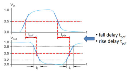
Fig 16 Time Delay
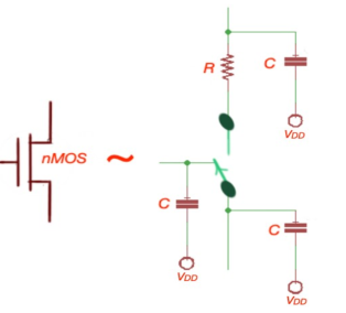
Fig 17 RC Circuit
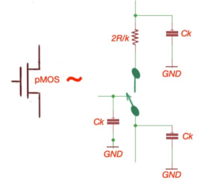
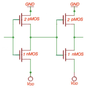
Fig 17: Equivalent RC circuits
The Elmore delay analysis model estimates the delay from a source (root) to one of the leaf nodes as the sum of the resistance in the path to the ith node multiplied by the capacitance present at the end of the branch.
Most circuits can be represented as an RC circuit with no loops. As we already stated, the Elmore delay estimates the delay from a source (root) to one of the leaf nodes as the sum of the resistance in the path to the ith node multiplied by the capacitance present at the end of the branch. In other words, the propagation delay from a switching source (root) to an ith branch node is given as the product of the capacitance “Ci” of the node with the sum of the resistance from the source to the node, Ris.
Tpd =
Ris = sum of resistance from source to node i
The 2nd order RC equivalent circuit we considered in the RC delay model:
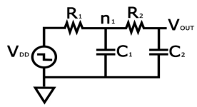
Fig 18 RC Equivalent
The Elmore delay for Vout is given as tpd = R1C1+(R1+ R2) C2, which is similar to the delay expression gotten for the two-time constant (TTC) approximation model we discussed in the last article.
Let's consider a driver—i.e., a gate that charges or discharges a node or, in other words, a gate that is connected to the input of another gate. For our example, we'll look at a driver which is w-times the unit size which is driving an m-identical inverter. The equivalent RC circuit is shown in Figure below
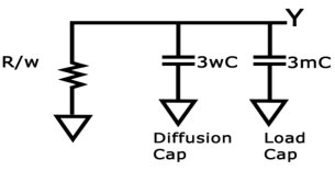
Fig 19 Equivalent Model

From above equation if we denote the fan-out of the drive to be the ratio between the load capacitance (3mc) and the input capacitance (3wc), we get the following:
h=3mc/3wc=m/w
Tpd = (1+h)3RC
Where τ=3RC.
Key takeaway
The Elmore delay analysis model estimates the delay from a source (root) to one of the leaf nodes as the sum of the resistance in the path to the ith node multiplied by the capacitance present at the end of the branch.
Normalized delay of a gate can be expressed as the sum of parasitic delay and effort delay. The effort delay depends on the fan-out of the gate, here is a logical effort.
Electrical effort is a situation when a gate is driving identical to itself gates is said to have an electrical effort or fan-out. In case if the load consists of gates different from driving gate, the electrical effort of fan-out can be found by formula, here is the capacitance of the driving gate, and is the capacitance of the load gates that are being driven.
Logical effort of the gate is the ratio of the input capacitance of the gate to the input capacitance of the inverter that delivers the same output current.
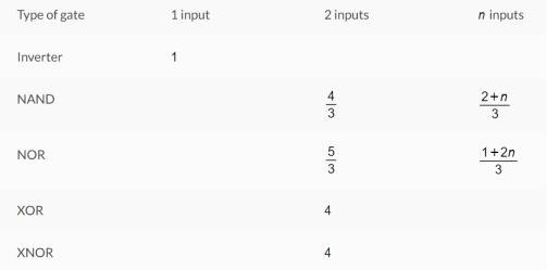
Parasitic delay is the delay when the gate drives zero load. It is comfortable to use the term of normalised parasitic delay, which is the ratio of diffusion capacitance to the gate capacitance of certain process.
The propagation delay of a logic gate e.g., inverter is the difference in time (calculated at 50% of input-output transition), when output switches, after application of input.
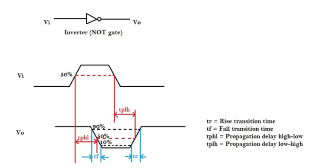
Fig 20 Propagation Delay
In the above figure, there are 4 timing parameters. Rise time (tr) is the time, during transition, when output switches from 10% to 90% of the maximum value. Fall time (tf) is the time, during transition, when output switches from 90% to 10% of the maximum value. Many designs could also prefer 30% to 70% for rise time and 70% to 30% for fall time. It could vary up to different designs.
The propagation delay high to low (tpHL) is the delay when output switches from high-to-low, after input switches from low-to-high. The delay is usually calculated at 50% point of input-output switching, as shown in above figure.
Now, in order to find the propagation delay, we need a model that matches the delay of inverter. As we have seen above, the switching behavior of CMOS inverter could be modelled as a resistance Ron with a capacitor CL, a simple first order analysis of RC network will help us to model the propagation delay.
Key takeaway
Delay in producing the output after application of input is called as delay.
The reduction in dimension of MOSFET or CMOS which reduces the size of chip is called as scaling. There are many advantages of scaling such as switching speed increases, chip size reduces and power dissipation reduces.
There are three types of scaling as constant voltage, constant field and lateral scaling. In constant voltage scaling, VDD is kept constant, and the process is scaled. For constant field scaling, the device dimensions are scaled by the parameter λ.
Constant Field Scaling:
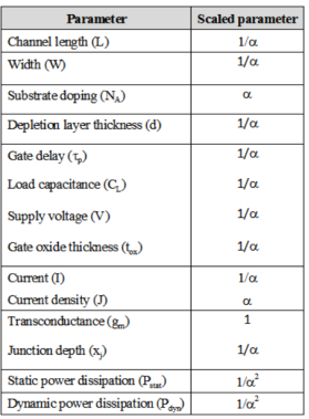
In constant field scaling the scaled devices are obtained by scaling all dimensions of transistor, device voltages and the doping concentration densities by factor . The effect of scaling is shown in Table below
Constant Voltage Scaling:
In constant voltage scaling the supply voltage VDD is kept constant while the process is scaled. The effect of scaling is shown in Table below.
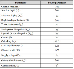
With constant voltage scaling the electric field increases which has led to the development of the lateral double diffused structures.
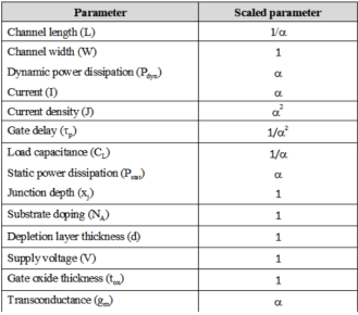
Lateral Scaling: In lateral scaling only the gate length is scaled. This is also called as the "gate shrinking". The effect of this scaling of parameters is shown in Table below.
Key takeaway
Scaling
- Increases the switching speed.
- Reduces chip size.
- Reduces power dissipation.
References:
1. Allen Holberg, “Analog CMOS Design”, Oxford University Press.
2. Neil H. E. Weste, David Money Harris, “CMOS VLSI Design: A Circuit & System
Perspective”, Pearson Publication