Unit - 3
SEQUENTIAL CIRCUIT DESIGN
The Bistability Principle:
Static memories use positive feedback to create a bistable circuit — a circuit having two stable states that represent 0 and 1.

Fig 1 Bistability
Multiplexer Based Latches
Multiplexer based latches can provide similar functionality to the SR latch, but has the important added advantage that the sizing of devices only affects performance and is not critical to the functionality.
Positive latch: When CLK=0 D input is passed to output, when CLK=1 input 1 is connected to output of latch.
Negative latch: When CLK=0 output is feedback to input, when CLK=1 input 1 D is selected.
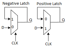
Fig 2 Multiplexer based latches
Master-Slave Based Edge Triggered Register:
When clock is low (CLK = 1), T1 is on and T2 is off, and the D input is sampled onto node QM.
When the clock goes high, the master stage stops sampling the input and goes into a hold mode.
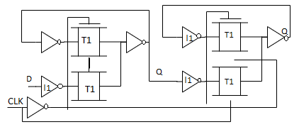
Fig 3 Master slave edge triggered register
Key takeaway
There are several fundamentally different approaches towards building a register. The most common and widely used approach is the master-slave configuration which involves cascading a positive latch and negative latch
Dynamic Transmission-Gate Based Edge-triggered Registers:
When CLK = 0, the input data is sampled on storage node 1, which has an equivalent capacitance of C1 consisting of the gate capacitance, the junction capacitance and the overlap gate capacitance of T2.
When CLK = 1, the transmission gate T2 turns on, and the value sampled on node 1 right before the rising edge propagates to the output Q.
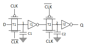
Fig 4 Dynamic latch
C2MOS Dynamic Register:
CLK = 0 (CLK = 1): The first tri-state driver is turned on, and the master stage acts as an inverter sampling the inverted version of D on the internal node X. The master stage is in the evaluation mode. Meanwhile, the slave section is in a high-impedance mode, or in a hold mode.
The roles are reversed when CLK = 1.
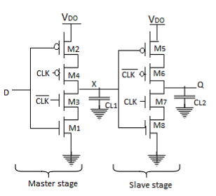
Fig 5 Dynamic Register
True Single-Phase Clocked Register (TSPCR):
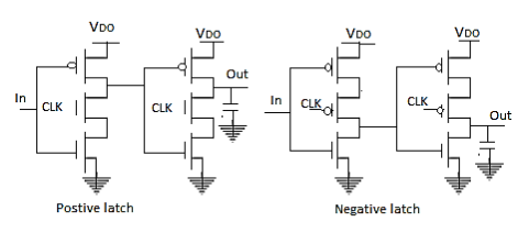
Fig 6 TSPCR
When CLK is high, the latch is in the transparent mode and corresponds to two cascaded inverters; the latch is non-inverting, and propagates the input to the output.
When CLK = 0, both inverters are disabled, and the latch is in hold-mode
Key takeaway
Registers can be static or dynamic. A static register holds state as long as the power supply is turned on. It is ideal for memory that is accessed infrequently (e.g., reconfiguration registers or control information). Dynamic memory is based on temporary charge store on capacitors. The primary advantage is the reduced complexity and higher performance/lower power. However, charge on a dynamic node leaks away with time, and hence dynamic circuits have a minimum clock frequency
We have used the master-slave configuration to create an edge-triggered register. A fundamentally different approach for constructing a register uses pulse signals. The idea is to construct a short pulse around the rising (or falling) edge of the clock. This pulse acts as the clock input to a latch (e.g., a TSPC flavor is shown in Figure a), sampling the input only in a short window. Race conditions are thus avoided by keeping the opening time (i.e., the transparent period) of the latch very short. The combination of the glitch generation circuitry and the latch results in a positive edge-triggered register. Figure b shows an example circuit for constructing a short intentional glitch on each rising edge of the clock. When CLK = 0, node X is charged up to VDD (MN is off since CLKG is low).
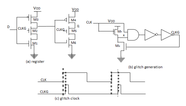
Fig 7 Glitch latch - timing generation and register.
On the rising edge of the clock, there is a short period of time when both inputs of the AND gate are high, causing CLKG to go high. This in turn activates MN, pulling X and eventually CLKG low (Figure c). The length of the pulse is controlled by the delay of the AND gate and the two inverters. Note that there exists also a delay between the rising edges of the input clock (CLK) and the glitch clock (CLKG) — also equal to the delay of the AND gate and the two inverters. If every register on the chip uses the same clock generation mechanism, this sampling delay does not matter. However, process variations and load variations may cause the delays through the glitch clock circuitry to be different. This must be taken into account when performing timing verification and clock skew analysis.
If set-up time and hold time are measured in reference to the rising edge of the glitch clock, the set-up time is essentially zero, the hold time is equal to the length of the pulse and the propagation delay (tc-q) equals two gate delays. The advantage of the approach is the reduced clock load and the small number of transistors required. The glitch-generation circuitry can be amortized over multiple register bits. The disadvantage is a substantial increase in verification complexity. This has prevented a wide-spread use.
Key takeaway
Registers can also be constructed using the pulse or glitch concept. An intentional pulse (using a one-shot circuit) is used to sample the input around an edge. Generally, the design of such circuits requires careful timing analysis across all process corners.
The figure below introduces another technique that uses a sense amplifier structure to implement an edge-triggered register. Sense amplifier circuits accept small input signals and amplify them to generate rail-to-rail swings. As we will see, sense amplifier circuits are used extensively in memory cores and in low swing bus drivers to amplify small voltage swings present in heavily loaded wires. There are many techniques to construct these amplifiers, with the use of feedback being one common approach.
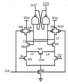
Fig 8 Positive edge-triggered register based on sense amplifier
The circuit shown in Figure above uses a precharged front-end amplifier that samples the differential input signal on the rising edge of the clock signal. The outputs of front-end are fed into a NAND cross-coupled SR FF that holds the data and guarantees that the differential outputs switch only once per clock cycle. The differential inputs in this implementation don’t have to have rail-to-rail swing and hence this register can be used as a receiver for a reduced swing differential bus.
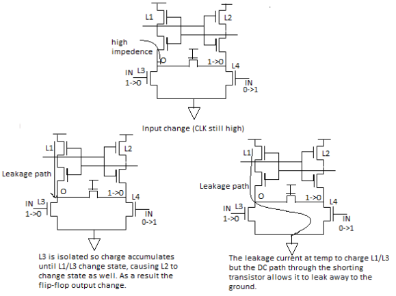
Fig 9 The need for the shorting transistor M4.
Uced swing differential bus. The core of the front-end consists of a cross-coupled inverter (M5-M8) whose outputs (L1 and L2) are precharged using devices M9 and M10 during the low phase of the clock. As a result, PMOS transistors M7 and M8 to be turned off and the NAND FF is holding its previous state. Transistor M1 is similar to an evaluate switch in dynamic circuits and is turned off ensuring that the differential inputs don’t affect the output during the low phase of the clock. On the rising edge of the clock, the evaluate transistor turns on and the differential input pair (M2 and M3) is enabled, and the difference between the input signals is amplified on the output nodes on L1 and L2. The cross-coupled inverter pair flips to one of its the stable states based on the value of the inputs. For example, if IN is 1, L1 is pulled to 0, and L2 remains at VDD. Due to the amplifying properties of the input stage, it is not necessary for the input to swing all the way up to VDD and enables the use of low swing signalling on the input wires.
The shorting transistor, M4, is used to provide a DC leakage path from either node L3, or L4, to ground. This is necessary to accommodate the case where the inputs change their value after the positive edge of CLK has occurred, resulting in either L3 or L4 being left in a high-impedance state with a logical low voltage level stored on the node. Without the leakage path that node would be susceptible to charging by leakage currents. The latch could then actually change state prior to the next rising edge of CLK as shown in above figure.
Key takeaway
Sense-amplifier based schemes are also used to construct registers and are to be used when high performance or low signal swing signalling is required.
- Pipelining is a popular design technique often used to accelerate the operation of the data paths in digital processors.
- Pipelining is a technique to improve the resource utilization, and increase the functional throughput.

Fig 10 Pipelining
Explanation:
- The combinational circuit block has been partitioned into three sections, each of which has a smaller propagation delay than the original function.
- Suppose that all logic blocks have approximately the same propagation delay, and that the register overhead is small with respect to the logic delays.
- This effectively reduces the value of the minimum allowable clock period:
Tmin,pipe = tc-q +max (tpd,add, tpd,abs,tpd,log)
- The increased performance comes at the relatively small cost of two additional registers, and an increased latency.
- The advantage of pipelined operation becomes apparent when examining the minimum clock period of the modified circuit
A Schmitt trigger is a device with two important properties:
- It responds to a slowly changing input waveform with a fast transition time at the output.
- The voltage-transfer characteristic of the device displays different switching thresholds for positive- and negative-going input signals. This is demonstrated in Figure below, where a typical voltage-transfer characteristic of the Schmitt trigger is shown (and its schematics symbol). The switching thresholds for the low-to-high and high to-low transitions are called VM+ and VM−, respectively. The hysteresis voltage is defined as the difference between the two.
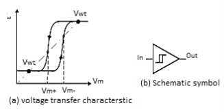
Fig 11 Non-inverting Schmitt trigger
One of the main uses of the Schmitt trigger is to turn a noisy or slowly varying input signal into a clean digital output signal. This is illustrated in Figure below. Notice how the hysteresis suppresses the ringing on the signal. At the same time, the fast low-to-high (and high-to-low) transitions of the output signal should be observed. For instance, steep signal slopes are beneficial in reducing power consumption by suppressing direct-path currents. The “secret” behind the Schmitt trigger concept is the use of positive feedback.
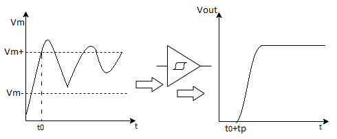
Fig 12 Noise suppression using a Schmitt trigger.
CMOS Implementation
The idea behind this circuit is that the switching threshold of a CMOS inverter is determined by the (kn/kp) ratio between the NMOS and PMOS transistors. Increasing the ratio results in a reduction of the threshold, while decreasing it results in an increase in VM. Adapting the ratio depending upon the direction of the transition results in a shift in the switching threshold and a hysteresis effect. This adaptation is achieved with the aid of feedback.
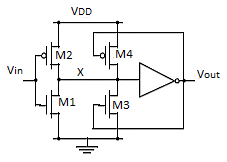
Fig 13 CMOS Schmitt Trigger
Suppose that Vin is initially equal to 0, so that Vout = 0 as well. The feedback loop biases the PMOS transistor M4 in the conductive mode while M3 is off. The input signal effectively connects to an inverter consisting of two PMOS transistors in parallel (M2 and M4) as a pull-up network, and a single NMOS transistor (M1) in the pull-down chain. This modifies the effective transistor ratio of the inverter to kM1/(kM2+kM4), which moves the switching threshold upwards. Once the inverter switches, the feedback loop turns off M4, and the NMOS device M3 is activated. This extra pull-down device speeds up the transition and produces a clean output signal with steep slopes. A similar behavior can be observed for the high-to-low transition. In this case, the pull-down network originally consists of M1 and M3 in parallel, while the pull-up network is formed by M2. This reduces the value of the switching threshold to VM–.
Key takeaway
Schmitt triggers display hysteresis in their dc characteristic and fast transitions in their transient response. They are mainly used to suppress noise.
A monostable element is a circuit that generates a pulse of a predetermined width every time the quiescent circuit is triggered by a pulse or transition event. It is called monostable because it has only one stable state (the quiescent one). A trigger event, which is either a signal transition or a pulse, causes the circuit to go temporarily into another quasi-stable state. This means that it eventually returns to its original state after a time period determined by the circuit parameters. This circuit, also called a one-shot, is useful in generating pulses of a known length. This functionality is required in a wide range of applications. We have already seen the use of a one-shot in the construction of glitch registers.

Fig 14 Transition-triggered one-shot
Another notorious example is the address transition detection (ATD) circuit, used for the timing generation in static memories. This circuit detects a change in a signal, or group of signals, such as the address or data bus, and produces a pulse to initialize the subsequent circuitry. The most common approach to the implementation of one-shots is the use of a simple delay element to control the duration of the pulse. The concept is illustrated in Figure above. In the quiescent state, both inputs to the XOR are identical, and the output is low. A transition on the input causes the XOR inputs to differ temporarily and the output to go high. After a delay t d (of the delay element), this disruption is removed, and the output goes low again. A pulse of length td is created. The delay circuit can be realized in many different ways, such as an RC-network or a chain of basic gates.
Key takeaway
Monostable structures have only one stable state. They are useful as pulse generators.
An astable circuit has no stable states. The output oscillates back and forth between two quasi-stable states with a period determined by the circuit topology and parameters. One of the main applications of oscillators is the on-chip generation of clock signals.
The ring oscillator is a simple, example of an astable circuit. It consists of an odd number of inverters connected in a circular chain. Due to the odd number of inversions, no stable operation point exists, and the circuit oscillates with a period equal to 2 × tp × N, with N the number of inverters in the chain and tp the propagation delay of each inverter.
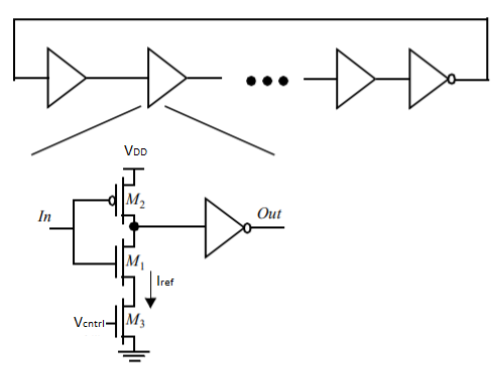
Fig 15 Voltage-controlled oscillator based on current-starved inverters.
The ring oscillator composed of cascaded inverters produces a waveform with a fixed oscillating frequency determined by the delay of an inverter in the CMOS process. In many applications, it is necessary to control the frequency of the oscillator. An example of such a circuit is the voltage-controlled oscillator (VCO), whose oscillation frequency is a function (typically non-linear) of a control voltage. The standard ring oscillator can be modified into a VCO by replacing the standard inverter with a current-starved inverter as shown in Figure above.
In this modified inverter circuit, the maximal discharge current of the inverter is limited by adding an extra series device. Here the low-to-high transition on the inverter can also be controlled by adding a PMOS device in series with M2. The added NMOS transistor M3, is controlled by an analog control voltage Vcntl, which determines the available discharge current. Lowering Vcntl reduces the discharge current and, hence, increases tpHL. The ability to alter the propagation delay per stage allows us to control the frequency of the ring structure. The control voltage is generally set using feedback techniques. Under low operating current levels, the current-starved inverter suffers from slow fall times at its output. This can result in significant short-circuit current. This is resolved by feeding its output into a CMOS inverter or better yet a Schmitt trigger. An extra inverter is needed at the end to ensure that the structure oscillates.
Key takeaway
Astable multivibrators, or oscillators, possess no stable state. The ring oscillator is the best-known example of a circuit of this class.
The setup time is the interval before the clock where the data must be held stable. The hold time is the interval after the clock where the data must be held stable. Hold time can be negative, which means the data can change slightly before the clock edge and still be properly captured. Most of the current day flip-flops has zero or negative hold time.
To avoid setup time violations:
- The combinational logic between the flip-flops should be optimized to get minimum delay.
- Redesign the flip-flops to get lesser setup time.
- Tweak launch flip-flop to have better slew at the clock pin, this will make launch flipflop to be fast there by helping fixing setup violations.
- Play with clock skew (useful skews).
To avoid hold time violations:
- By adding delays (using buffers).
- One can add lockup-latches (in cases where the hold time requirement is very huge, basically to avoid data slip).
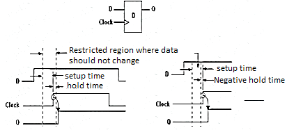
Fig 16 Timing Diagram
Asynchronous sequential circuits
If some or all the outputs of a sequential circuit do not change affect with respect to active transition of clock signal, then that sequential circuit is called as Asynchronous sequential circuit. That means, all the outputs of asynchronous sequential circuits do not change affect at the same time. Therefore, most of the outputs of asynchronous sequential circuits are not in synchronous with either only positive edges or only negative edges of clock signal.
Synchronous sequential circuits
If all the outputs of a sequential circuit change affect with respect to active transition of clock signal, then that sequential circuit is called as Synchronous sequential circuit. That means, all the outputs of synchronous sequential circuits change affect at the same time. Therefore, the outputs of synchronous sequential circuits are in synchronous with either only positive edges or only negative edges of clock signal.
Sequencing Elements
Latch: Level sensitive
– a.k.a. Transparent latch, D latch
Flip-flop: edge triggered
– master-slave flip-flop, D flip-flop, D register
Timing Diagrams
– Transparent – Opaque – Edge-trigger
Latch Design
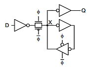
Buffered output +
Widely used in standard cells
+ Very robust (most important)
- Rather large
- Rather slow (1.5 – 2 FO4 delays)
- High clock loading
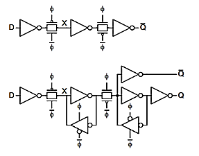
Flip-Flop Design
Flip-flop is built as pair of back-to-back latches
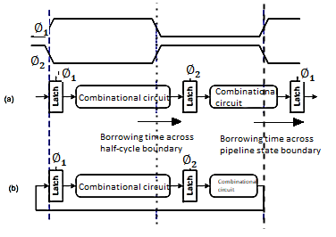
Time Borrowing
In a flop-based system:
– Data launches on one rising edge
– Must setup before next rising edge
– If it arrives late, system fails
– If it arrives early, time is wasted
– Flops have hard edges
In a latch-based system
– Data can pass through latch while transparent
– Long cycle of logic can borrow time into next
– As long as each loop completes in one cycle
References:
1. D.A. Pucknell, K. Eshraghian, ‘Basic VLSI Design’, 3rd Edition, Prentice Hall of India, New Delhi,
2003.
2. Debprasad Das, VLSI Design, Oxford University Press, 2010.
3. Eugene D. Fabricius, ‘Introduction to VLSI Design’, Tata McGraw Hill, 1990.
4. Impact of DFM and RET on Standard-Cell Design Methodology by Paul de Dood, Rahul Saxena, Deepak Sharma, Sachin Kalra, Azeem Hasan, Vikas Garg
Freescale Semiconductors Ltd