Unit - 5
IMPLEMENTATION STRATEGIES AND TESTING
The field-programmable gate array (FPGA) is an integrated circuit that consists of internal hardware blocks with user-programmable interconnects to customize operation for a specific application.
FPGA architecture consists of thousands of fundamental elements called configurable logic blocks (CLBs) surrounded by a system of programmable interconnects, called a fabric, that routes signals between CLBs. Input/output (I/O) blocks interface between the FPGA and external devices.
Depending on the manufacturer, the CLB may also be referred to as a logic block (LB), a logic element (LE) or a logic cell (LC).
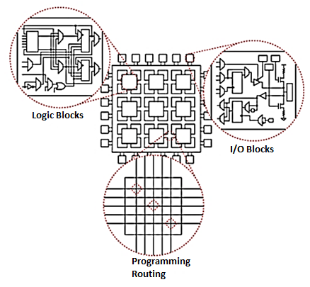
Fig.1: FPGA architecture
An individual CLB is made up of several logic blocks. A lookup table (LUT) is a characteristic feature of an FPGA. An LUT stores a predefined list of logic outputs for any combination of inputs: LUTs with four to six input bits are widely used. Standard logic functions such as multiplexers (mux), full adders (FAs) and flip-flops are also common.
The number and arrangement of components in the CLB varies by device.
It contains two three-input LUTs an FA and a D-type flip-flop plus a standard mux and two muxes, that are configured during FPGA programming.
This simplified CLB has two modes of operation. In normal mode, the LUTs are combined with Mux 2 to form a four-input LUT; in arithmetic mode, the LUT outputs are fed as inputs to the FA together with a carry input from another CLB.
Current-generation FPGAs include more complex CLBs capable of multiple operations with a single block; CLBs can combine for more complex operations such as multipliers, registers, counters and even digital signal processing (DSP) functions.
Key takeaway
FPGA architecture consists of thousands of fundamental elements called configurable logic blocks (CLBs) surrounded by a system of programmable interconnects, called a fabric, that routes signals between CLBs. Input/output (I/O) blocks interface between the FPGA and external devices.
Global routing
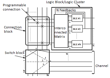
- The global router performs a coarse route to determine, for each connection, the minimum distance path through routing channels that it has to go through.
- If the net to be routed has more than two terminals the global router will break the net into a set of two-terminal5 connections and route each set independently.
- The global router considers for each connection multiple ways of routing it and chooses the one that passes through the least congested routing channels.
- The principal objective of the global router, balancing the usage of the routing channels, is achieved.
- Once all connections have been coarse routed, the solution is optimized by ripping up and rerouting each connection a small number of times.
- After that, the final solution is passed to the detailed router
Detail routing
- Detail routing algorithms construct a directed graph from the routing resources to represent the available connection between wires, C blocks, S blocks and logic blocks within the FPGA.
- The paths are labeled according to a cost function that takes into account the usage of each wire segment and the distance of the interconnecting points.
- The distance is estimated by calculating the wire length in the bounding box of the interconnecting points.
- This is done to avoid subsequent iterations of ripping out and re-routing if the solution lies on the near outside of the bounding box.
Test engineers usually have to construct test vectors after the design is completed. This invariably requires a substantial amount of time and effort that could be avoided if testing is considered early in the design flow to make the design more testable. As a result, integration of design and test, referred to as design for testability (DFT), was proposed in the 1970s. To structurally test circuits, we need to control and observe logic values of internal lines. Unfortunately, some nodes in sequential circuits can be very difficult to control and observe; for example, activity on the most significant bit of an n bit counter can only be observed after 2"“' clock cycles. Testability measures of controllability and observability were first defined in the 1970s to help find those parts of a digital circuit that will be most difficult to test and to assist in test pattern generation for fault detection. Many DFT techniques have been proposed since that time. DFT techniques generally fall into one of the following three categories:
(1) Ad hoc DFT techniques
(2) Level-sensitive scan design (LSSD) or scan design
(3) Built-in self-test (BIST)
Ad hoc DFT Techniques
Ad hoc testing combines a collection of tricks and techniques that can be used to increase the observability and controllability of a design and that are generally applied in an application-dependent fashion. An example of such a technique is illustrated in Fig. (a), which shows a simple processor with its data memory. Under normal configuration, the memory is only accessible through the Processor. Writing and reading a data value into and out of a single memory position requires a number of clock cycles.
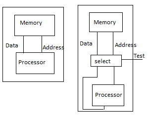
The controllability and observability of the memory can be dramatically improved by add multiplexers on the data and address buses (Fig.). During normal operation mode, these selectors direct the memory ports to the processor. During test, the data and address ports are connected directly to the I/O pins, and testing the memory can proceed more efficiently. The example illustrates some important design-for testability concepts.
It is often worthwhile to introduce extra hardware that has no functionality except improving the testability. Designers are often willing to incur a small penalty in area and performance if it makes the design substantially more observable or controllable. Design-for-testability often means that extra I/O pins must be provided besides die nominal functional I/O pins. The test port in Fig.(b) is such an extra pin. To reduce the number of extra pads that would be required, one can multiplex test signals and functional signals on the same pads. For example, the I/O bus in Fig. (b) serves as a data bus during normal operation and provides and collects the test patterns during testing.
An extensive collection of ad hoc test approaches has been devised. Examples include the partitioning of large state machines, addition of extra test points, prevision of reset states, and introduction of test buses. While very effective, the applicability of most of these techniques depends upon the application and architecture at hand. The insertion into a given Hating requires expert knowledge and is difficult to automate. Stricture and automatable approaches are more desirable.
Key takeaway
DFT techniques generally fall into one of the following three categories:
(1) Ad hoc DFT techniques
(2) Level-sensitive scan design (LSSD) or scan design
(3) Built-in self-test (BIST)
Objectives of Scan Design
- Scan design is implemented to provide controllability and observability of internal state variables for testing a circuit.
- It is also effective for circuit partitioning.
- A scan design with full controllability and observability turns the sequential test problem into a combinational one.
Scan Design Requirements
- Circuit is designed using pre-specified design rules. Test structure (hardware) is added to the verified design.
- One (or more) test control (TC) pin at the primary input is required.
- Flip-flops are replaced by scan flip-flops (SFF) and are connected so that they behave as a shift register in the test mode. The output of one SFF is connected to the input of next SFF. The input of the first flip-flop in the chain is directly connected to an input pin (denoted as SCANIn), and the output of the last flipflop is directly connected to an output pin (denoted as SCANOUT). In this way, all the flip-flops can be loaded with a known value, and their value can be easily accessed by shifting out the chain. Figure 39.1 shows a typical circuit after the scan insertion operation.
- Input/output of each scan shift register must be available on PI/PO.
- Combinational ATPG is used to obtain tests for all testable faults in the combinational logic.
- Shift register tests are e applied and ATPG tests are converted into scan sequences for use in manufacturing test.
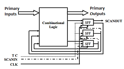
Fig 2 Scan structure to a design
Figure above shows a scan structure connected to design. The scan flip-flips (FFs) must be interconnected in a particular way. This approach effectively turns the sequential testing problem into a combinational one and can be fully tested by compact ATPG patterns. Unfortunately, there are two types of overheads associated with this technique that the designers care about very much. These are the hardware overhead (including three extra pins, multiplexers for all FFs, and extra routing area) and performance overhead (including multiplexer delay and FF delay due to extra load).
Scan Design Rules
- Only clocked D-type master-slave flip-flops for all state variables should be used.
- At least one PI pin must be available for test. It is better if more pins are available.
- All clock inputs to flip-flops must be controlled from primary inputs (PIs). There will be no gated clock. This is necessary for FFs to function as a scan register.
- Clocks must not feed data inputs of flip-flops. A violation of this can lead to a race condition in the normal mode.
Scan Overheads
- The use of scan design produces two types of overheads. These are area overhead and performance overhead. The scan hardware requires extra area and slows down the signals.
- IO pin overhead: At least one primary pin necessary for test.
- Area overhead: Gate overhead = [4 nsff/(ng+10nff)] x 100%, where ng = number of combinational gates; nff = number of flip-flops; nsff = number of scan flip-flops; For full scan number of scan flip-flops is equal to the number of original circuit flip-flops. Example: ng = 100k gates, nff = 2k flip-flops, overhead = 6.7%. For more accurate estimation scan wiring and layout area must be taken into consideration.
- Performance overhead: The multiplexer of the scan flip-flop adds two gate-delays in combinational path. Fanouts of the flip-flops also increased by 1, which can increase the clock period.
As the complexity of VLSI circuits increases, test generation and application become an expensive and not always very effective means of testing. Built-in Self-Test (BIST) is another solution.
It is a mechanism that permits a machine to test itself. Engineer’s design BISTs to meet requirements such as:
- High reliability
- Lower repair cycle times
Or constraints such as:
- Limited technician accessibility
- Cost of testing during manufacture
The main purpose of BIST is to reduce the complexity, and thereby decrease the cost and reduce reliance upon external (pattern-programmed) test equipment.
It reduces cost in two ways:
- Reduces test-cycle duration
- Reduces the complexity of the test/probe setup, by reducing the number of I/O signals that must be driven/examined under tester control.
Figure below shows the Built-in Self-Test system.
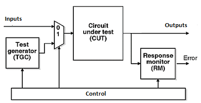
Figure 3. BIST
Advantages:
- Lower cost due to elimination of external tester
- In-system, at-system, high-quality testing
- Faster fault detection, ease of diagnosis
- Overcomes pin limitations and related interfacing problems
- Reduces maintenance and repair costs at system level.
IDDQ testing refers to the integrated circuit (IC) testing method based upon measurement of steady state power-supply current. Iddq stands for quiescent Idd, or quiescent power-supply current. Today, the majority of IC’s are manufactured using complementary metal–oxide–semiconductor (CMOS) technology. In steady state, when all switching transients are settled-down, a CMOS circuit dissipates almost zero static current. The leakage current in a defect-free CMOS circuit is negligible (on the order of few nanoamperes). However, in case of a defect such as gate-oxide short or short between two metal lines, a conduction path from power-supply (Vdd) to ground (Gnd) is formed and subsequently the circuit dissipates significantly high current. This faulty current is a few orders of magnitude higher than the fault-free leakage current. Thus, by monitoring the power-supply current, one may distinguish between faulty and fault-free circuits.
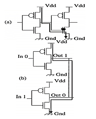
Fig 4 Formation of current path in presence of gate-oxide short and metal bridging in CMOS circuit.
This concept is illustrated in Fig (a) shows CMOS inverters with a gate-oxide short and Fig. 1 shows two CMOS inverters with shorted outputs. The current conduction paths formed due to these defects are also highlighted in Fig(a) and (b). As suggested by Figure above, the concept of Iddq testing is very simple, however, its implementation in today's very large-scale integrated circuits (VLSI) is not so straightforward. This paper covers the present state of this technology and provides necessary details on all essential items. The rest of the introduction section is devoted to the historical background and answering the question why this method has drawn attention and became a buzzword in the semiconductor test industry. These sub-sections essentially provide the motivation to study this technology.
Key takeaway
IDDQ testing refers to the integrated circuit (IC) testing method based upon measurement of steady state power-supply current. Iddq stands for quiescent Idd, or quiescent power-supply current.
In emerging technology nodes, manufacturability becomes a more and more severe issue, even with various resolution enhancement techniques, e.g., optical proximity correction (OPC), phase shift mask (PSM), and sub-resolution assist feature (SRAF) insertion. To overcome the manufacturing problem and improve circuit yield, several early design stages should be aware of the manufacturing constraints. In this section, we discuss how manufacturability can be seamlessly considered in four physical and mask design stages: standard cell design, placement, routing, and mask optimization.
DFM is a systems approach to improving the competitiveness of a manufacturing enterprise by developing products that are easier, faster, and less expensive to make, while maintaining required standards of functionality, quality, and marketability. Design for manufacturability (DFM) and early manufacturing involvement (EMI) concepts are now major components of the development effort designed to maintain and enhance the rate of technology advancement and significantly improve the development-to-manufacturing transition. Design-for-manufacturability philosophy and practices are used in many companies because it is recognized that 70% to 90% of overall product cost is determined before a design is ever released into manufacturing. The semiconductor industry continues to grow in both complexity and competitiveness.
Problem Statement
The layout development is most critical in integrated circuits (IC's) design because of cost, since it involves expensive tools and a large amount of human intervention, and also because of the consequences for production cost. As the device size is shrinking, the landscape of technology developments has become very different from the past. The problems, which were supposed to be secondary can cause of yield drop out in submicron technologies. The variability becomes a critical issue not only for performance, but also for yield dropout.
Yield dropout due to given below defects.
1. Random Defects: Due to form of impurities in the silicon itself, or the introduction of a dust particle that lands on the wafer during processing. These defects can cause a metal open or shorts. As feature sizes continue to shrink, random defects have not decreased accordingly making advanced IC’s even more susceptible to this type of defect.
2. Systematic Defects: Again, systematic defects are more prominent contributor in yield loss in deep submicron process technologies. Systematic defects are related to process technology due to limitation of lithography process which increased the variation in desired and printed patterns. Another aspect of process related problem is planarity issues make layer density requirements necessary because areas with a low density of a particular layer can cause upper layers to sag, resulting in discontinuous planarity across the chip.
3. Parametric Defects: In deep submicron technology parametric defects is most critical for us. Parametric defects come into the picture due to improper modeling of interconnects parasitic. As a result, manufactured device does not match the expected result from design simulation and does not meet the design specification.
Design for manufacturability (DFM) is process to overcome these defects of yield drop out. The DFM will not be done without collaborations between various technology parties, such as process, design, mask, EDA, and so on. The DFM will give us a big challenge and opportunity in nanometer era.
DESIGN FOR MANUFACTURABILITY:
Design for Manufacturability is the proactive process which ensures the quality, reliability, cost effective and time to market.
DFM consist a set of different methodologies trying to enforce some soft (recommended/Mandatory) design rules regarding the shapes and polygons of the physical layout which improve the yield.
Given a fixed amount of available space in a given layout area, there are potentially multiple yield enhancing changes that can be made.
There are some DFM guidelines which we can take into account during layout.
Antenna effect guidelines
Configuration: Identify poly gates connected to large areas of metals.
Action: Reduce the ratio surface of metal/surface poly gate or use free wheel diode.
Reasons for this action: During process, the wafers are submitted to plasma environments. Because of metallization, electrons are collected. Because of mirror effects charges accumulate at the gate oxide. An electric field is created and can cause oxide breakdown.
Minimum Area of physical layers
Configuration: Identify very small rectangle of a given layer (typically shape at the min area size like diffusion)
Action: Try not to draw shapes at min area when free space is available around.
Reasons for this action: Process window can allow shapes to be at min area, but if these shapes are numerous, risk is higher that some of them are not resolved: for instance, in case of implant, that would lead to missing implant. Typical case: Pwell and Nwell Straps (Ties).
Density Gradient
Configuration: Identify high density areas next to low density areas.
Action: Try to balance shapes to reach homogeneous density and add dummy patterns.
Reasons for this action: Density of some layers (specifically those treated by Chemical & Mechanical Polishing (CMP) like diffusion, poly and metals) has a big impact on the manufacturing of the given pattern. Impact is both on CMP processing and PHOTO processing. Too high gradient can lead to shorts or opens.
Contact Enclosure by Diffusion/poly silicon
Configuration: Identify min enclosure of contacts by diffusion.
Action: Try to extend the enclosure of contact by diffusion area when possible.
Reasons for this action: Overlay could make that one contact falls on the border of the diffusion area, thus generating a junction leakage.
Caution: Proportions of the dimensions of this transistor have not been kept, for a better visibility of the example. Take care of resulting increase of drain capacitance.
Metal extension of Via/contact at Line Ends
Configuration: Identify Via transitions at line ends.
Action: Try to extend the overlap of metals at line ends.
Reasons for this action: Process window issues might lead to resistive or even open vias. Extending metals overlap ensures a better transition.
Gate Extension on Diffusion (End Cap)
Configuration: Identify poly gate of transistor at min from diffusion.
Action: Try to extend the poly end cap wherever it is not too close to other structures
Reasons for this action: Silicon implementation of this configuration could lead to leakage current between drain and source of the given transistor. Do not draw at min if space is available.
Contact/Via Redundancy
Configuration: Identify single contact specifically for critical transistor in repetitive cell.
Action: Try to double contact and extend poly and metal1 without impacting too much on poly & metal1 critical area.
Reasons for this action: Single contacts can be more sensitive to defect and resistivity spread especially in case of L transition. Salicide discontinuity risk is also present. Inserting a new contact reduces probability to have a too resistive (or even open) transition, and reduces electro-migration effect.
Metal to Metal spacing
Configuration: Identify wires at min spacing with free space around
Action: Do not keep min spacing. Try to spread these wires and if not possible decrease width/space ratio.
Reasons for this action: Long wires at min spacing increase probability to have shorts due to particles.
Key takeaway
DFM is a systems approach to improving the competitiveness of a manufacturing enterprise by developing products that are easier, faster, and less expensive to make, while maintaining required standards of functionality, quality, and marketability. Design for manufacturability (DFM) and early manufacturing involvement (EMI) concepts are now major components of the development effort designed to maintain and enhance the rate of technology advancement and significantly improve the development-to-manufacturing transition.
Boundary scan is a method for testing interconnects (wire lines) on printed circuit boards or sub-blocks inside an integrated circuit. Boundary scan is also widely used as a debugging method to watch integrated circuit pin states, measure voltage, or analyse sub-blocks inside an integrated circuit.
Testing
The boundary scan architecture provides a means to test interconnects and clusters of logic, memories etc. Without using physical test probes. It adds one or more so called 'test cells' connected to each pin of the device that can selectively override the functionality of that pin. These cells can be programmed via the JTAG scan chain to drive a signal onto a pin and across an individual trace on the board. The cell at the destination of the board trace can then be programmed to read the value at the pin, verifying the board trace properly connects the two pins. If the trace is shorted to another signal or if the trace has been cut, the correct signal value will not show up at the destination pin, and the board will be observed to have a fault.
On-Chip Infrastructure
To provide the boundary scan capability, IC vendors add additional logic to each of their devices, including scan cells for each of the external traces. These cells are then connected together to form the external boundary scan shift register (BSR), and combined with JTAG TAP (Test Access Port) controller support comprising four (or sometimes more) additional pins plus control circuitry. Some TAP controllers support scan chains between on-chip logical design blocks, with JTAG instructions which operate on those internal scan chains instead of the BSR. This can allow those integrated components to be tested as if they were separate chips on a board.
On-chip debugging solutions are heavy users of such internal scan chains. These designs are part of most Verilog or VHDL libraries. Overhead for this additional logic is minimal, and generally is well worth the price to enable efficient testing at the board level. For normal operation, the added boundary scan latch cells are set so that they have no effect on the circuit, and are therefore effectively invisible. However, when the circuit is set into a test mode, the latches enable a data stream to be shifted from one latch into the next. Once a complete data word has been shifted into the circuit under test, it can be latched into place so it drives external signals. Shifting the word also generally returns the input values from the signals configured as inputs.
Test Mechanism
As the cells can be used to force data into the board, they can set up test conditions. The relevant states can then be fed back into the test system by clocking the data word back so that it can be analysed. By adopting this technique, it is possible for a test system to gain test access to a board. As most of today’s boards are very densely populated with components and tracks, it is very difficult for test systems to physically access the relevant areas of the board to enable them to test the board. Boundary scan makes access possible without always needing physical probes. In modern chip and board design, Design for Test is a significant issue, and one common design artifact is a set of boundary scan test vectors, possibly delivered in Serial Vector Format (SVF) or a similar interchange format.
JTAG Test Operations
Devices communicate to the world via a set of input and output pins. By themselves, these pins provide limited visibility into the workings of the device. However, devices that support boundary scan contain a shift-register cell for each signal pin of the device. These registers are connected in a dedicated path around the device's boundary (hence the name). The path creates a virtual access capability that circumvents the normal inputs and provides direct control of the device and detailed visibility at its outputs. He contents of the boundary scan are usually described by the manufacturer using a part-specific BSDL file. Among other things, a BSDL file will describe each digital signal exposed through pin or ball (depending on the chip packaging) exposed in the boundary scan, as part of its definition of the Boundary Scan Register (BSR). A description for two balls might look like this:
"541 (bc_1, *, control, 1)," &
"542 (bc_1, GPIO51_ATACS1, output3, X, 541, 1, Z)," & "543 (bc_1
, GPIO51_ATACS1, input, X)," &
"544 (bc_1, *, control, 1)," &
"545 (bc_1, GPIO50_ATACS0, output3, X, 544, 1, Z)," & "546 (bc_1,
GPIO50_ATACS0, input, X)," &
That shows two balls on a mid-size chip (the boundary scan includes about 620 such lines, in a 361-ball BGA package), each of which has three components in the BSR: a control configuring the ball (as input, output, what drive level, pullups, pulldowns, and so on); one type of output signal; and one type of input signal. There are JTAG instructions to SAMPLE the data in that boundary scan register, or PRELOAD it with values. During, testing, I/O signals enter and leave the chip through the boundary-scan cells. Testing involves a number of test vectors, each of which drives some signals and then verifies that the responses are as expected.
The boundary-scan cells can be configured to support external testing for interconnection between chips (EXTEST instruction) or internal testing for logic within the chip (INTEST instruction).
Board Test Infrastructure
Typically, high-end commercial JTAG testing systems allow the import of design 'netlists' from CAD/EDA systems plus the BSDL models of boundary scan/JTAG complaint devices to automatically generate test applications. Common types of tests include
- Scan-path 'infrastructure' or integrity
- Boundary-scan device pin to boundary-scan device pin 'interconnect'
- Boundary-scan pin to memory device or device cluster (SRAM, DRAM, DDR etc)
- Arbitrary logic cluster testing
When used during manufacturing, such systems also support non-test but affiliated applications such as in-system programming of various types of flash memory: NOR, NAND, and serial (I2C or SPI). Such commercial systems are used by board test professionals and will often cost several thousand dollars for a fully-fledged system.
They can include diagnostic options to accurately pin- point faults such as open circuits and shorts and may also offer schematic or layout viewers to depict the fault in a graphical manner. Tests developed with such tools are frequently combined with other test systems such as in-circuit testers (ICTs) or functional board test systems.
Key takeaway
Boundary scan is a method for testing interconnects (wire lines) on printed circuit boards or sub-blocks inside an integrated circuit. Boundary scan is also widely used as a debugging method to watch integrated circuit pin states, measure voltage, or analyse sub-blocks inside an integrated circuit.
References:
1. D.A. Pucknell, K. Eshraghian, ‘Basic VLSI Design’, 3rd Edition, Prentice Hall of India, New Delhi,
2003.
2. Debprasad Das, VLSI Design, Oxford University Press, 2010.
3. Eugene D. Fabricius, ‘Introduction to VLSI Design’, Tata McGraw Hill, 1990.
4. Impact of DFM and RET on Standard-Cell Design Methodology by Paul de Dood, Rahul Saxena, Deepak Sharma, Sachin Kalra, Azeem Hasan, Vikas Garg
Freescale Semiconductors Ltd