Unit - 1
The 741 IC Op-Amp
This IC is an 8 pin IC in the dual in line (DIP) package. This is the one of the oldest and one of the most popular Op-amp IC. It is a high performance monolithic operational amplifier [5]. It has wide range of applications such as integrator, differentiator, summing amplifier etc.
DEFINITION OF 741-PIN FUNCTIONS
Pin 1 (Offset Null): Offset voltage is nulled by application of a voltage of opposite polarity to the offset.
Pin 2 (Inverted Input): All input signals at this pin will be inverted at output pin 6.
Pin 3 (Non-Inverted Input): All input signals at this pin will be processed normally without inversion.
Pin 4 (-V): The V- pin (also referred to as Vcc) is the negative supply voltage terminal.
Pin 5 (Offset Null): Same pin 1.
Pin 6 (Output): Output signal's polarity will be the opposite of the input's when this signal is applied to the op-amp's inverting input.
Pin 7 (+V): The V+ pin (also referred to as Vcc) is the positive supply voltage terminal of the 741 Op-Amp IC.
Pin 8 (N/C): The 'N/C' stands for 'Not Connected'. There is no other explanation. There is nothing connected to this pin, it is just there to make it a standard 8-pin package.
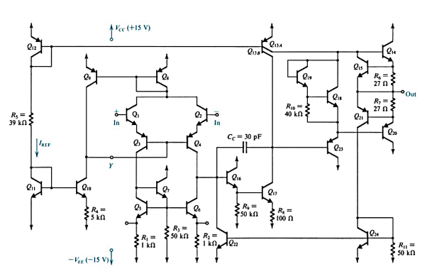
Fig 1: The 741 op-amp circuit. Q11, Q12, and R5 generate a reference bias current, IREF. Q10, Q9, and Q8 bias the input stage, which is composed of Q1 to Q7. The second gain stage is composed of Q16 and Q17 with Q13B acting as active load. The class AB output stage is formed by Q14 and Q20 with biasing devices Q13A, Q18, and Q19, and an input buffer Q23. Transistors Q15, Q21, Q24, and Q22 serve to protect the amplifier against output short circuits and are normally cut off.
Bias Circuit
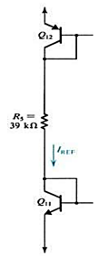
The reference bias current of the 741 circuit, IREF, is generated in the branch at the extreme left of Fig. 1, Q11 and Q12 and the resistance R5.
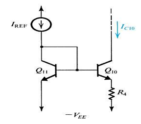
Widlar current source is formed by Q11 and Q10 and the resistance R4. The bias current for the first stage is generated in the collector of Q10.
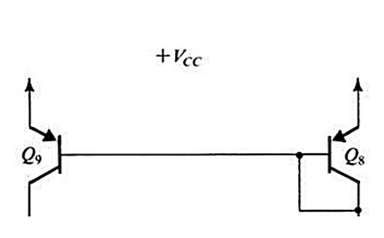
- There is another current mirror formed by Q8 and Q9 which is responsible for the biasing in the first stage.
- Q13 is double-collector lateral pnp transistor.
- The transistors Q12 and Q13 form a two-output current mirror.
- Collector of Q13A provides the bias current for the output stage of the op amp.
- The purpose of Q18 and Q19 is to establish the two VBE drops between the bases of the output transistors Q14 and Q20.
Short Circuit Protection Circuitry
- The 741 circuit includes large number of transistors that are normally off and conduct only when large output current is required.
- The large current can be achieved at the output terminals if the output terminal is short-circuited to one of the two supplies.
- This circuit protects the IC if an excess load current is drawn from it.
- The short-circuit protection network consists of R6, R7, Q15, Q21, Q24, R11 and Q22.
Input Stage
- Input stage consists of transistors through Q1 to Q7.
- The biasing is performed by transistors Q8, Q9 and Q10.
- Transistors Q5, Q6 and Q7 and resistors R1, R2 and R3 form the load circuit of the input stage.
- Every OP-AMP circuit uses a level shifter.
- The function of level shifter is to shift the dc level of the signal so that the signal at the OP-AMP output can swing positive and negative.
- In 741, level shifting is done in the first stage using the lateral pnp transistors Q3 and Q4.
Second Stage
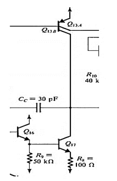
- The second stage or intermediate stage is composed of Q16, Q17, Q13B, and two resistors R8 and R9.
- Transistor Q16 acts as an emitter follower.
- So, it provides high input resistance to the second stage.
- This minimizes the loading on the input stage and avoids the loss of gain.
- Transistor Q17 acts as a common-emitter amplifier with a 100 Ώ resistance in its emitter.
- Its load is composed of the high output resistance of the pnp current source Q13B in parallel with the input resistance with the output stage.
- The output of the second stage is taken at the collector of Q17.
- Capacitor CC is connected in the feedback path of the second stage to provide frequency compensation.
- Capacitor CC is small in value.
- The chips are for Capacitor CC is about 13 times that of a standard npn transistor
The Output Stage
- 741 uses class AB output stage.
- The purpose of the output stage is to provide the amplifier with low output resistance.
- Emitter follower circuit is the class A output stage.
- The drawback of the class A output stage is large power dissipated in the transistor.
- This power dissipation can be reduced by arranging the transistor to turn on only when an input signal is applied.
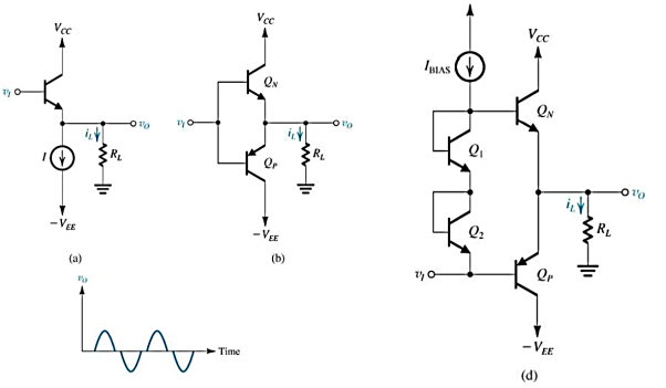
Fig 2 (a) The emitter follower is a class A output stage. (b) Class B output stage (c) The output of a class B output stage fed with an input sinusoid. Observe the crossover distortion. (d) Class AB output stage.
- So, in order to reduce the power dissipation two transistors are required.
- A npn to source the output current and a pnp transistor to sink the output current.
- This kind of arrangement is called class B output stage.
- Both the transistors will be cut off when vI = 0.
- When vI goes positive QN conducts while QP remains off.
- When vI goes negative transistors reverse roles.
- Class B output stage is efficient in power dissipation, but the output signal is distorted
- Output signal is distorted when |vI|is less than about 0.5, neither of the transistors will conduct. This is called crossover distortion.
- Crossover distortion can be reduced by biasing the output stage transistors at low current.
- In this case, the output stage transistors will remain conducting when vI is small.
The Device Parameters
- For the standard npn and pnp transistors, the following parameters will be used:
- Npn: Is = 10-14 A, β = 200, VA = 125 V
- Pnp: Is = 10-14 A, β = 50, VA = 50 V In 741 circuit the nonstandard devices are Q13, Q14 and Q20.
- For transistor Q13, ISA = 0.25x10⁻¹⁴ A ISB = 0.75x10⁻¹⁴ A,
- Transistors Q14 and Q20 have an area three time that of a standard device.
Key takeaway
This IC is an 8 pin IC in the dual in line (DIP) package. This is the one of the oldest and one of the most popular Op-amp IC. It is a high performance monolithic operational amplifier [5]. It has wide range of applications such as integrator, differentiator, summing amplifier etc.
DC Analysis
- For the dc analysis of an op-amp circuit, the Input terminals are grounded.
- This should result in zero dc voltage at the output.
- However, because the op amp has very large gain, the output voltage is close to either +VCC or –VEE.
- To overcome this problem, In the dc analysis, it will be assumed that the op amp is connected in a negative feedback loop that stabilizes the output dc voltage to zero volts.
Reference Bias Current
The reference Bias current IREF can be obtained as:
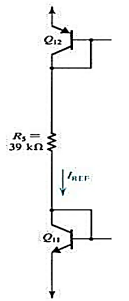

For VCC = VEE = 15 V and VBE12 = VEB12 = 0.7 V, we have IREF = 0.73 mA.
Input Stage Bias
Transistor Q11 is biased by IREF, and the voltage developed across it is used to bias Q10 which has a series emitter resistance R4.
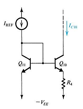
Fig 3 The Widlar current source that biases the input stage
From the circuit, and assuming β10 to be large,
We have,

Now assume that, IS11=IS10 we get,

At room temperature VT = 25 mV.
For our case IC10 = 19 µA.
Input Bias and Offset Current
The input bias current of an op amp is defined as

For the 741 we obtain

Because of possible mismatches in the β values of Q1 and Q2 the input base currents will not be equal.
In this case, input offset current is defined as,

Second Stage Bias
If we neglect the base current of Q23, then we see that the collector current of Q17 is approximately equal to the current supplied by current source Q13B.
Because Q13B, has a scale current 0.75 times that of Q12.
Its collector current will be IC13B ≈ 0.75IREF, where we have assumed that βP >>1.
Thus IC13B = 550µA & IC17 ≈ 550µA.
Base-emitter voltage of Q17 is

The collector current of Q16 is given as,

Which gives, IC16 = 16.2µA
Output Bias Stage
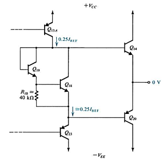
Fig 4 The 741-output stage without the short -circuit protection devices.
Current source Q13A delivers a current of 0.25IREF (because IS of Q13A is 0.25 times the IS of Q12).
Neglecting base currents of Q14 & Q20,
IC23 ≈ IE23 ≈ 0.25IREF = 180 µA.
If we assume that VBE18 is approximately 0.6 V. We can determine the current in R10 as 15 µA.
The emitter current of Q18 is therefore
IE18 ≈ IC18 = 180 - 15 = 165 µA & VBE18 = 588 mV.
The base current IB18 = 165/200 = 0.8 µA. So,
IC19 ≈ IE19 = 15.8 µA
VBE19 is determined as

As, we know that the purpose of the transistors Q18 - Q19 network is to provide two VBE drops between the bases of the output transistors Q14 & Q20.
This voltage drop VBB is given by


Now putting values of VBB, and IS14 = IS20 = 3x10- 14 A, we get, IC14 = IC20 = 154 µA.
This is the small current at which class AB output stage is biased.
AC analysis
The Input Stage
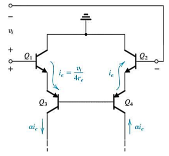
Fig 5 Small-signal analysis of the 741-input stage
The differential signal vI applied between the input terminals.
The four transistors shown in figure are connected in series.
Emitter signal currents flow as indicated in Fig.

Where re is emitter resistance of the four transistors shown in figure. Where,

Input differential resistance is given by

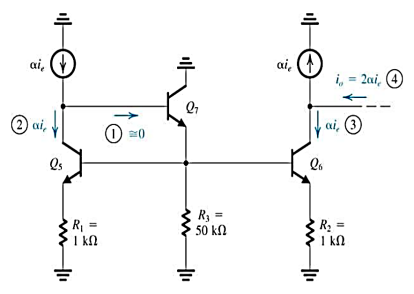
Fig 6 The load circuit of the input stage fed by the two complementary current signals generated by Q1 through Q4 in Fig. Shown on previous slide Circled numbers indicate the order of the analysis steps.
Assuming the base current of Q7 to be equal to zero, so the collector current of Q5 will be,

Transistors Q5 and Q6 are identical and have identical emitter resistances, therefore,

So, the load circuit behaves like a current mirror.
Consider output node of the input stage, the output current is given by,

Transconductance of the input stage is given by,

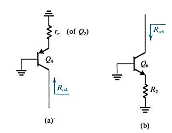
Fig 7 Simplified circuits for finding the two components of the output resistance Ro1 of the first stage.
- Output resistance (R01) of the input stage is the resistance seen looking back onto the collector of transistor Q6.
- From the figure 6, we can say that, R01 is equal to the parallel combination of the output resistance of the current source ie and the output resistance of Q6.
- Assume that the base of Q4 is virtual ground. The R04 is given by,

- So, for Q4, re=2.63 kΩ, ro =VA /I, VA= 50V, I = 9.5 µA, rπ = (β+1)re>>re, so neglecting it.
- So, R04 = 10.5 MΩ.
- The R04 is given by,
- So, for Q4, re= 2.63 kΩ, ro =VA /I, VA= 50V, I = 9.5 µA, rπ = (β+1)re>>re, so neglect it.
- So, R06 = 18.2 MΩ. Hence, the output resistance of the input stage is given by, R01 = 6.7 MΩ
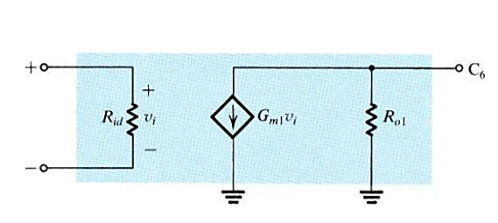
Fig 8 Small-signal equivalent circuit for the input stage of the 741Op Amp.
The Second Stage
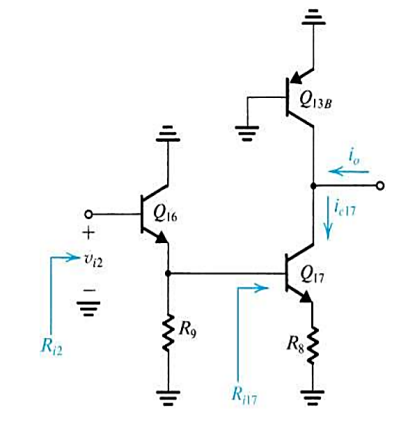
Fig 9 The 741 second stage prepared for small-signal analysis
This is used to determine the values of the parameters of the equivalent circuit.
Input Resistance: The resistance Ri2 is given by

So, Ri2 = 4MΩ.

Fig 10 Small-signal equivalent circuit model of the second stage.
Transconductance: from the small-signal equivalent circuit model of the second stage, we can observe that,


So, Gm2 = 6.5 mA/V
Output Resistance: output resistance of the second stage is given by,

Where, R013B = re13, for 741 re13 = 90.9 kΩ.
Where,

R017 = 787kΩ
Therefore, R02 = 81kΩ.
The Output Stage
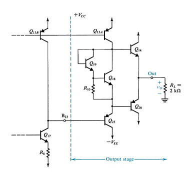
Fig 11 The 741-output stage
The above figure shows the output stage.
Gain
The overall small-signal gain can be found from the cascade of the equivalent circuits.

Fig 12 Cascading the small-signal equivalent circuits of the individual stages for the evaluation of the overall voltage gain.
Load resistance RL = 2 kΩ.
The overall gain can be expressed as,

So,

Key takeaway
For AC analysis the output differential gain is given by
Ad = vo/vid = RC/re
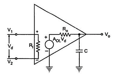
Fig 13 High frequency model of OP-AMP
- Frequency response of the op-amp is the plot of its open loop gain versus frequency.
- The open loop gain changes with frequency.
- To plot the frequency response, we need to refer high frequency model of OP-AMP.
- After a certain frequency the roll-off decreases after certain frequency.
- The capacitor is due to BJT used in the 741.
- The BJTs has parasitic capacitances so the capacitances are too small.
- So, in order to reduces the effect of this parasitic capacitances the compensated capacitor is used in 741.
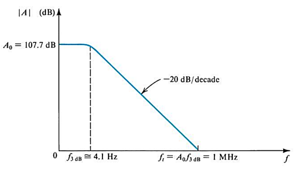
Fig 14 Frequency Response
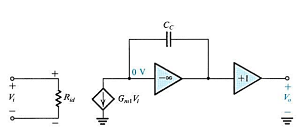
- In simplified model of 741, the high-gain second stage, with its feedback capacitance CC is modeled by an ideal integrator.
- In this model, the gain of the second stage is assumed to be very large.
- That’s why the output resistance of the input stage and the input resistance of the second stage have been omitted.
- The output stage is assumed to be an ideal unity gain follower.


The magnitude of the gain becomes unity at ω=ωt
Where:

So,

Where, ft is called unity gain frequency.
At f >> f3dB, the gain falls off with a slope of 20dB/decade, just like an integrator.
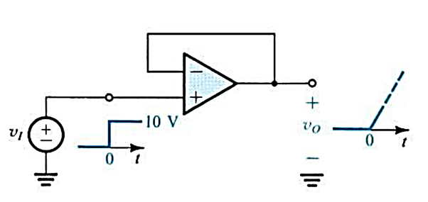
- Consider the unity-gain follower shown on previous slide.
- 10-volt step is applied at the input.
- The entire value of the step signal will appear as a differential signal between the two input terminals.
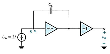
From the circuit shown on previous slide, we see that, output voltage ramp with a slope of 2I/CC.

So, the slew rate is given by

For 741 SR = 0.63 V/µs.
Relationship between ft and SR can be found by

As we know that

So, 
So,

And we get

Finally, we get,

Solved Examples
Q1) Estimate dc emitter current in each transistor of differential amplifier shown in fig. How much is dc voltage from each collector to ground? How much is Vout?
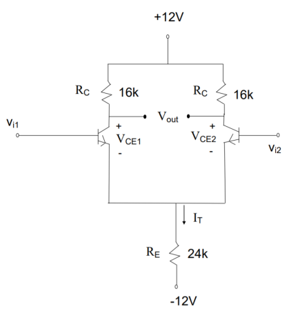
Sol:
The tail current through 24k resistor is,


The emitter current, IE, in each transistor is


Since IC = IE, voltage summation in the output circuit gives,


Then

Q2) Design an inverter amplifier with gain of 120 and input impedance of 5kΩ. Give the circuit.
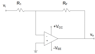
Sol: Figure shows the circuit for an inverting amplifier.
Since for an inverting amplifier, the input impedance Zi is,
Zi = R1 = 5kΩ (desired)
Therefore, R1 = 5kΩ Further, the gain AV of inverting amplifier is,
Av =RF/Ri
And, AV desired is 120, R1 = 5kΩ
Therefore, RF = AV x R1 = 120 X 5k= 600 kΩ
Q3) Find out the voltage gain of the non-inverting amplifier shown in fig.
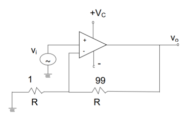
Sol: The voltage gain of a non-inverting amplifier is,


Q4) In the amplifier circuit shown in fig., if open loop gain and open loop band width of the op amp respectively are 105 and 10 HZ, Calculate the bandwidth of feedback amplifier
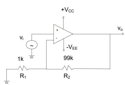
Sol: If open loop band width is f2, the band width with feedback, f2(FB) is given by f2(FB) = f2(1 + AB) ≈ f2. AB because AB>>1 Now, A = 105 (given) And the gain of feedback network, B in the circuit shown in fig. Is
And the gain of feedback network, B in the circuit shown in fig. Is

Then,


Q5) For the summing amplifier shown in fig., estimate the values of resistors R1, R2 and R3 so that the output V0 is, V0 = - (3V1 + V2 + 0.2V3). What is the approximate value of the compensating resistor R?
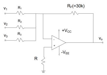
Sol:
The output voltage,  for the summing amplifier is,

Thus, for the desired output,

Similarly,


And 


And


Q6) Determine the output voltage in the circuit shown in fig. If Va= 5V, Vb= -2V and Vc = 3b
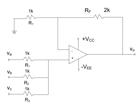
Sol: In the amplifier circuit shown in fig. Since the resistors R1, R2, and R3 are all equal to 1kΩ, the voltage V1, at non-inverting input terminal will be average of the three voltages, Va, Vb, and Vc. Thus,


And the gain for non-inverting amplifier, AV, is


Q7) Differential gain Ad, of an op amp measures 100. In the measurement of common mode gain experiment when 1.0V is applied common to both the inputs, output voltage measured is 0.01V. How much is common-mode rejection ratio (CMRR)?
A7) By definition, common mode rejection ratio (CMRR) is

Where Ad is gain in differential mode which is given as 100.
And, the gain in common mode, ACM is,

Therefore,


Q8) 8 Figure shows a low-pass filter. Calculate the value of feedback resistor RF so that band-pass gain is 100. Also calculate the value of resistor R to get cut-off frequency of 2kHZ.
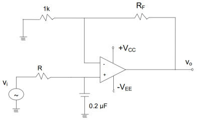
Sol: The gain in band-pass region is that of non-inverting amplifier and it is,

 then
then


The cut-off frequency, f, for low-pass fitter is given by


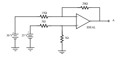
Q9) For the difference amplifier circuit shown, determine the output voltage at terminal A.
Sol:
By voltage division,

By the virtual short circuit between the input terminals, vin- = 9.375 V Using Ohm's law, the current through the 15 Ω resistor is

The input impedance is infinite; therefore, Iin-=0 and I15=I20. Use Kirchoff's voltage law to find the
Output voltage at A.

Q10) What is the current, i?
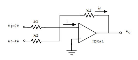
Sol: The input current of IDEAL op amp is very small. Hence, it is considered to be 0. So, i=0A
Q11) What is the output voltage, vo? For circuit shown in Q10)
Sol: This op amp circuit is a summing amplifier. Since i=0,

 ) (8
) (8
Q12) For the ideal op amp shown, what should be the value of resistor Rf to obtain a gain of 5?
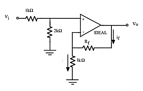
Sol: By voltage division

By the virtual short circuit


Since the op amp draws no current, if=i

But, vo = 5vi.


Q13) Evaluate the following amplifier circuit to determine the value of resistor R4 in order to obtain a voltage gain (vo/vi) of -120
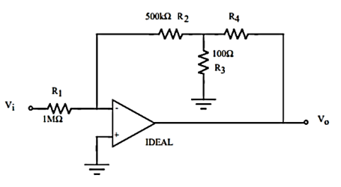
Sol:
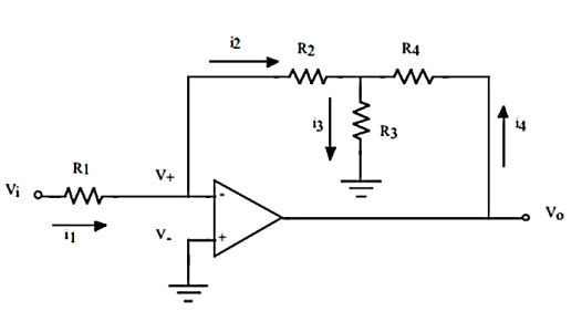
vin+ is grounded, so vin- is also a virtual ground.
vin- = 0
Since vin- = 0, vi=i1Rl and il=vi/R1.
Since vin- = 0, vx=-i2R2 and i2=-vx/R2.
Similarly, vx=-i3R3
vx-vo =-i4R4
From Kirchhoff's current law, i4 = i2 + i3

Now, vo=-120vi.
Also, il=i2, so


Q14) For the circuit shown below If Rf = 1MW and Ri=50W, what is the voltage gain?
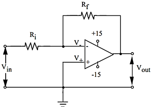
Sol: There are two ways to solve any problem involving an op amp. The first way is to use

Where va is the input to the inverting terminal and vb is the input to the non-inverting terminal. In this case, there is no input to the non-inverting input and vb=0. The formula reduces to the simple result

Using the given circuit values, we get

The voltage gain is then -20,000. Note that any value over 100 is impractical for any real amplifier. A more general way of solving any op amp circuit is to note that an ideal (and most real) op amps must satisfy the virtual short assumption, i.e., that V+=V-. Using this assumption and KCL at an input node is adequate to solve most any op amp problem. In this case, KCL at the inverting input gives


So, we get the same result. Note that any value over 100 is impractical for any real amplifier
Q15) For the circuit shown below, If Vin=0.1 volts, what is Vout?
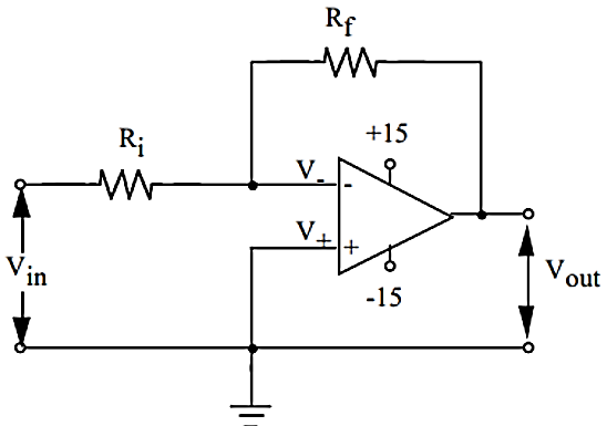
Sol: Solve same as above question We get vo = – 20,000vin = – 20,000 (0.1 volts) = – 2000 volts. As mentioned previously, this is a ridiculous value for an output.
Q16) For the circuit shown below, V1 = 10sin 200t and V2 = 15sin 200t. What is Vout? The op amp is ideal with infinite gain.
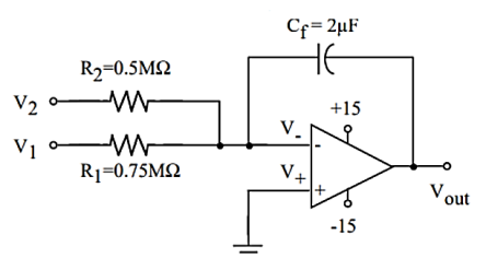
Sol: Any problem with a capacitor (or inductor) in it and sinusoidal voltages immediately indicates that phasors are required. This means that V1 and V2 should be represented as phasors, and Cf should be replaced by an impedance. This problem is not solved very well with the formulas in the Reference Handbook. This circuit is most easily solved using the virtual short assumption (V+=V-), and using KCL at the inverting input. Note that the grounding of V+ then requires that V-=0. This is also called the virtual short assumption.

Rationalizing this expression gives

Solving for Vout gives

It is important to recognize that all sine functions should always be converted to cosines for proper phase in the phasor expressions, i.e., sin 200t = cos (200t – 90)0 ´ 1- 90 = –j
Using the circuit parameters given,


The answer is then

References:
1. Gayakwad: Op-Amps and Linear Integrated Circuits, 4th Edition Prentice Hall of India, 2002.
2. Franco, Analog Circuit Design: Discrete & Integrated, TMH, 1st Edition.
3. Salivahnan, Electronics Devices and Circuits, TMH, 3rd Edition, 2015
4. Millman and Halkias: Integrated Electronics, TMH, 2nd Edition, 2010
5. UNIT III – IC 741 OP-AMP By: Ajay Kumar Gautam Asst. Prof. ECED, DBITW, Dehradun