Unit - 5
Integrated Circuit Timer
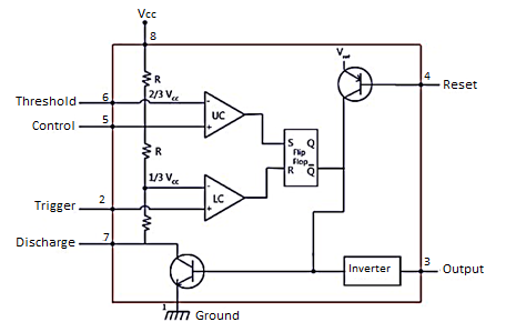
Fig 1 IC 555 Timer
For IC555 timer working as a flip flop or as a multi-vibrator, it has a particular set of configurations. Some of the major features include:
- It operates from a wide range of power ranging from +5 Volts to +18 Volts supply voltage.
- Sinking or sourcing 200 mA of load current.
- The external components should be selected properly so that the timing intervals can be made into several minutes along with the frequencies exceeding several hundred kilohertz.
- The output of a 555 timer can drive a transistor-transistor logic (TTL) due to its high current output.
- It has a temperature stability of 50 parts per million (ppm) per degree Celsius change in temperature which is equivalent to 0.005 %/ °C.
- The duty cycle of the timer is adjustable.
- Also, the maximum power dissipation per package is 600 mW and its trigger and reset inputs has logic compatibility.
Key takeaway
They can be used as frequency divider, PWM, SR F/F, missing pulse detection etc.
The 555 generally operates in 3 modes:
- A-stable
- Mono-stable
- Bi-stable modes.
Astable mode
This means there will be no stable level at the output. So, the output will be swinging between high and low. This character of unstable output is used as a clock or square wave output for many applications.
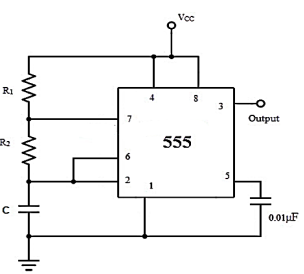
Fig 2 Astable Multivibrator
It is self-triggered multivibrator as pin 2 and 6 are connected. The supply is given through pin 8 and the output is obtained through pin 3. The timer will be reset if a low signal is given to pin 4. The capacitor is connected across pin 5 so that the external noise or any dc level are filtered. The resistor pair R1 and R2 form a circuit for determining the width of the output pulse.
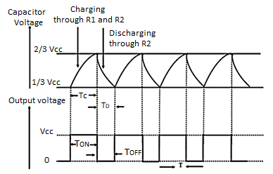
Fig 3 Capacitor and Output voltage waveform
During charging the capacitor charges through R1 and R2 and voltage across capacitor rises exponentially and during discharging the capacitor discharges through R2 and voltage falls exponentially. The output is obtained across pin 3.
The time for which capacitor charges from 1/3VCC to 2/3VCC is equal to the time the output is high which is given by
tc= 0.69(R1+R2) C
The discharging time from 2/3Vcc to 1/3VCC is given as
td= 0.69 R2C
The total period of output waveform is given by
T = tc+ td = 0.69(R1+2R2) C
The frequency of oscillations is given by
f0 =  =
= 
The duty cycle is defined as the ratio of the charging time of capacitor at which the output is high to the total time period.
% Duty cycle =  x 100
x 100
Applications of Astable Multivibrator
Square wave Oscillator: The astable multivibrator shown in the figure below [Ref.1] can be used to generate square wave oscillations. The diode is connected across RB and the diode and capacitor are charged through RA to a voltage of 2/3 of VCC. The capacitor discharges through RB and Q1. The discharging of capacitor when reaches 1/3VCC the discharging stops.
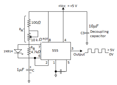
Fig 4 Astable multivibrator as square wave oscillator
Free-Running Ramp Generator
The circuit diagram is shown below [Ref.1]. The transistor Q1 is turned on by the comparator 1 when voltage across capacitor is 2/3Vcc. The capacitor C discharges through Q1. When capacitor discharges the voltage across C is 1/3Vcc, comparator 2 turns off Q1. The time period is given as
T = VCCC/3IC
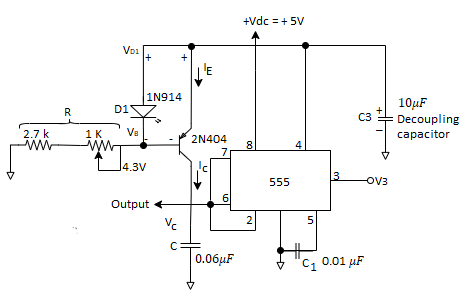
Fig 5 Free Running Ramp generator circuit
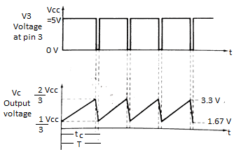
Fig 6 Output waveform
IC = (VCC-VBE)/R
The free running frequency of ramp generator is given by
f0 = 3IC/VCCC
The output waveform is shown in above figure.
Mono-stable mode
This configuration consists of one stable and one unstable state. The stable state can be chosen either high or low by the user.
If the stable output is set at high (1), the output of the timer is high (1). At the application of an interrupt, the timer output turns low (0). Since the low state is unstable it goes to high (1) automatically after the interrupt passes. The monostable multivibrator using IC555 is shown below.
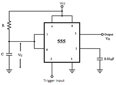
Fig 7 Monostable multivibrator using 555
The output is taken through pin 3. The supply is connected to pin 8. A small capacitor is connected to filter noise. The working is shown below in figure and explained as well.
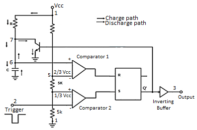
Fig 8 555 connected as monostable multivibrator
The discharge transistor will go to saturation when the F/F is reset. The discharge of C takes place through drain of CMOS. During negative pulse comparator 2 compares the pulse with reference voltage of 1/3 Vcc and output is low until the input becomes greater than the reference voltage. The output of F/F is set high when the output goes below 1/3Vcc. The output at pin 3 is high.
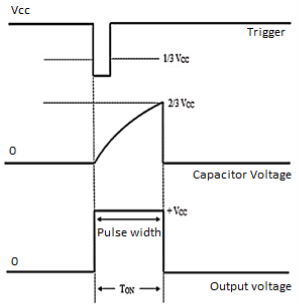
Fig 9 Input and Output waveform
When the C discharges the transistor is off and the voltage decays exponentially. This is input to the comparator 1 with reference voltage 2/3Vcc. The output is still high obtained at pin 3. The output of comparator is high when the threshold voltage becomes more than the reference voltage. Due to this the F/F is reset and output goes to zero. When the output is low the capacitor discharges completely and the transistor goes into saturation.
Pulse width
The voltage across C is Vc = Vcc (1-e-t/RC)
When voltage across capacitor is 2/3Vcc
2/3Vcc = Vcc (1-e-t/RC)
e-t/RC= 1/3
Taking log of both sides and solving we get
t= 1.098RC
The pulse width of rectangular pulse is 1.1RC (approx.)
Application of Monostable Multivibrator
Frequency Divider
The monostable multivibrator can be used as frequency divider by adjusting the time interval off charging. The charging time is made larger than the period of input pulse the device acts as divide-by-2 network. By proper selection of R and C the timing interval can be controlled. The waveform is shown below.
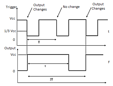
Fig 10 Divide-by-2 circuit waveform
When negative input pulse is applied the output goes high and will remain high irrespective of any other input pulse application as the timing interval s greater than the time period of trigger pulse. The circuit is triggered for every alternate negative going pulse.
Pulse Stretcher
This application makes use of the fact that output pulse width of monostable multivibrator is larger than the negative pulse width of trigger pulse. The output of monostable multivibrator is the stretched form of the input pulse. The pulse stretcher is shown below.
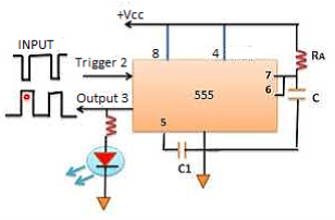
Fig 11 Pulse Stretcher
Example-1
An Astable 555 Oscillator is constructed using the following components, R1 = 1kΩ, R2 = 2kΩ and capacitor C = 10uF. Calculate the output frequency from the 555 oscillator and the duty cycle of the output waveform.
t1 – capacitor charge “ON” time is calculated as:
t1 = 0.693(R1 + R2). C
= 0.693(1000 +2000) x 10 x 10 -6 = 0.021 s= 0.21 msec
t2 – capacitor discharge “OFF” time is calculated as:
t2 = 0.693 R2. C
= 0.693 X 2000 x 10 x 10 -6 = 14ms
Total periodic time (T) is therefore calculated as:
T = t1 + t2 = 21 ms + 14 ms = 35 ms.
The output frequency, ƒ is therefore given as:
f = 1/T = 1/35ms = 28.6 Hz
Giving a duty cycle value of:
Duty Cycle = R1 + R2 / (R1 + 2 R2) = 1000 + 2000/ (1000 + 2 x 2000) = 60%
Key takeaways
Sr. No. | Astable multivibrator | Monostable Multivibrator | Bistable multivibrator |
1. | There are no stable states of output | There is only one stable state of the output | There are two stable states of the output. |
2. | Trigger input is not necessary for changing the state of the output | Trigger pulse is required for changing the state of output | Trigger pulse is required for changing the state of output |
3. | Used as rectangular, square wave or ramp generator. | Used as timer. | Used as flip-flop. |
4. | Number of quasi-stable state is 2. | Number of quasi-stable state is 1. | No quasi-stable state. |
5. | Time of for the two quasi stable depends on RC time constant. The two quasi stable states can have different intervals. | Time for the quasi-stable state depends on RC time constant. | No quasi-stable states. |
Voltage controlled oscillator is a type of oscillator where the frequency of the output oscillations can be varied by varying the amplitude of an input voltage signal. Voltage controlled oscillators are commonly used in frequency (FM), pulse (PM) modulators and phase locked loops (PLL).
Another application of the voltage-controlled oscillator is the variable frequency signal generator itself.
The block diagram of a typical voltage-controlled oscillator is shown below.

Fig 12 Block Diagram of VCO
Voltage controlled oscillators can be broadly classified into a linear voltage-controlled oscillators and relaxation type voltage-controlled oscillators. Linear voltage-controlled oscillators are generally used to produce a sine wave. In such oscillators, an LC tank circuit is used for producing oscillations. An active element like a transistor is used for amplifying the output of the LC tank circuit, compensating the energy lost in the tank circuit and for establishing the necessary feedback conditions. Here a varactor (varicap) diode is used in place of the capacitor in the tank circuit. A varactor diode is a type of semiconductor diode whose capacitance across the junction can be varied by varying the voltage across the junction. Thus by varying the voltage across the varicap diode in the tank circuit, the output frequency of the VCO can be varied.
Relaxation-type voltage controlled oscillators are used to produce a sawtooth or triangular waveform. This is achieved by the gradual charging and sudden discharge of a capacitor connected appropriately to an active element (UJT, PUT etc) or a monolithic IC (LM566 etc). Nowadays relaxation type VCOs are generally realized using monolithic ICs
Pin Diagram
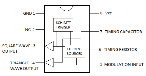
Fig 13 Pin Diagram of IC 566
Pin Description:
Pin 1: Ground (GND)
Pin 2: No connection (NC)
Pin 3: Square wave output
Pin 4: Triangular wave output
Pin 5: Modulation input
Pin 6: Timing resistor
Pin 7: Timing capacitor
Pin 8: Vcc
Applications:
Function generator
Tone generator
FM modulation
Frequency shift keying
Clock generator
Voltage controlled oscillator using LM566 IC
LM566 is a monolithic voltage-controlled oscillator from National Semiconductors. It can be used to generates square and triangle waveforms simultaneously. The frequency of the output waveform can be adjusted using an external control voltage. The output frequency can be also programmed using a set of external resistor and capacitor.
Typical applications of LM566 IC are signal generators, FM modulators, FSK modulators, tone generators etc. The LM566 IC can be operated from a single supply or dual supply. While using a single supply, the supply voltage range is from 10V to 24V. The IC has a very linear modulation characteristic and has excellent thermal stability. The circuit diagram of a voltage-controlled oscillator using LM566 is shown in the figure below.
Circuit Diagram
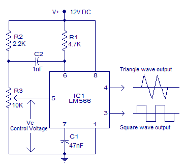
Fig 14 Circuit Diagram of IC 566
Working
Resistor R1 and capacitor C1 form the timing components. Capacitor C2 is used to prevent the parasitic oscillations during VCO switching. Resistor R3 is used to provide the control voltage Vc. Triangle and square wave outputs are obtained from pins 4 and 3 respectively. The output frequency of the VCO can be obtained using the following equation:
Fout = 2.4(V+-V5) /(R1C1V+).
Where Fout is the output frequency, R1 and C1 are the timing components and V+ is the supply voltage.
Key takeaway
Features:
The maximum operating voltage is 10V to 24V
High-temperature stability
Operating temperature is 0˚C to 70˚C
The frequency can be controlled using current, voltage, resistor or capacitor
Power dissipation is 300mV
Excellent power supply rejection
5.4.1 Basic principle of PLL
A phase-locked loop consists of a phase detector and a voltage-controlled oscillator. The output of the phase detector is the input of the voltage-controlled oscillator (VCO) and the output of the VCO is connected to one of the inputs of a phase detector which is shown below in the basic block diagram. When these two devices are feed to each other the loop forms.
5.4.2 Block diagram, Working
A basic phase locked loop, PLL, consists of three basic elements:
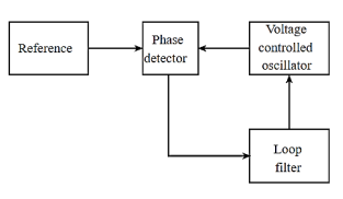
Fig 15 Block Diagram of PLL
- Phase comparator / detector: As the name implies, this circuit block within the PLL compares the phase of two signals and generates a voltage according to the phase difference between the two signals.
- Voltage controlled oscillator, VCO: The voltage-controlled oscillator is the circuit block that generates the radio frequency signal that is normally considered as the output of the loop. Its frequency can be controlled over the operational frequency band required for the loop.
- Loop filter: This filter is used to filter the output from the phase comparator in the phase locked loop, PLL. It is used to remove any components of the signals of which the phase is being compared from the VCO line, i.e., the reference and VCO input. It also governs many of the characteristics of the loop including the loop stability, speed of lock, etc.
Operation
The diagram for a basic phase locked loop shows the three main element of the PLL: phase detector, voltage- controlled oscillator and the loop filter.
In the basic PLL, reference signal and the signal from the voltage- controlled oscillator are connected to the two input ports of the phase detector.
The output from the phase detector is passed to the loop filter and then filtered signal is applied to the voltage- controlled oscillator.
The Voltage Controlled Oscillator, VCO, within the PLL produces a signal which enters the phase detector. The phase of the signals from the VCO and the incoming reference signal are compared and a resulting difference or error voltage is produced. This corresponds to the phase difference between the two signals.
The error signal from the phase detector passes through a low pass filter which governs many of the properties of the loop and removes any high frequency elements on the signal.
Once through the filter the error signal is applied to the control terminal of the VCO as its tuning voltage. The sense of any change in this voltage is such that it tries to reduce the phase difference and hence the frequency between the two signals.
Initially the loop will be out of lock, and the error voltage will pull the frequency of the VCO towards that of the reference, until it cannot reduce the error any further and the loop is locked.
When the PLL, phase locked loop, is in lock a steady state error voltage is produced. By using an amplifier between the phase detector and the VCO, the actual error between the signals can be reduced to very small levels.
However, some voltage must always be present at the control terminal of the VCO as this is what puts onto the correct frequency.
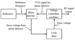
Fig 16 PLL showing voltages
The fact that a steady error voltage is present means that the phase difference between the reference signal and the VCO is not changing. As the phase between these two signals is not changing means that the two signals are on exactly the same frequency.
Key takeaways
The phase locked loop has three main elements: phase detector, voltage- controlled oscillator and the loop filter. When the PLL, phase locked loop, is in lock a steady state error voltage is produced. By using an amplifier between the phase detector and the VCO, the actual error between the signals can be reduced to very small levels.
One of the main areas where phase detectors are used is within phase locked loops, although this is by no means the only one.
The phase detector enables phase differences to be detected and the resultant "error" voltage to be produced.
There are different types of phase detector. They can be categorised in a variety of ways, but one is given below:
- Phase only sensitive detectors
- Phase / frequency detectors
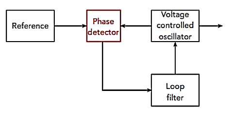
Fig 15 Block Diagram
Phase only sensitive detectors
Phase detectors that are only sensitive to phase are the most straightforward form of phase detector. As the name indicates their output is only dependent upon the phase difference between the two signals. When the phase difference between the two incoming signals is steady, they produce a constant voltage. When there is a frequency difference between the two signals, they produce a varying voltage at a frequency equal to the frequency difference.
The difference frequency product is the one used to give the phase difference. However, it is quite possible that the difference frequency signal will fall outside the pass-band of the loop filter, and hence the overall phase locked loop. If this occurs then no error voltage pass through the PLL loop filter and on to the Voltage Controlled Oscillator, VCO, to bring it into lock. This means that there only is a limited range over which the phase locked loop can be brought into lock. This range is called the capture range. Once in lock the loop can generally be pulled over a much wider frequency band.
Apart from using a phase frequency detector, there are several ways in which this problem can be overcome. The oscillator must be steered close to the reference oscillator frequency. This can be achieved in a number of ways. One is to reduce the tuning range of the oscillator so that the difference product will always fall within the pass-band of the loop filter. In other instances, another tune voltage can be combined with the feedback from the loop to ensure that the oscillator is in the correct region. This is approach is often adopted in microprocessor systems where the correct voltage can be calculated for any given circumstance.
XOR phase detector: The exclusive OR, XOR phase detector circuit can provide a very useful simple phase detector for some applications. It comprises of a logic exclusive OR circuit. Being digital in format it can often fit into a phase locked loop with ease as many of the circuits associated with the phase locked loop may already be in a digital format. Alternatively, an exclusive OR can be made from discrete components to give a wider variety of levels and other options.
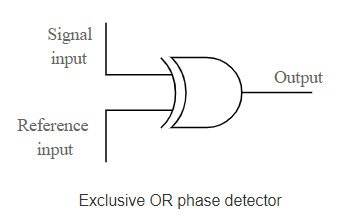
Fig 16 Ex-OR phase Detector
The way in which an exclusive OR, XOR phase detector works can be seen by the diagram below:
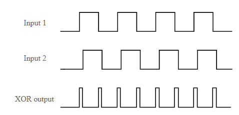
Fig 17 EX-OR Phase Detector Response Waveform
It can be seen that using these waveforms, the XOR logic gate can be used as a simple but effective phase detector.
As might be expected for such a simple circuit, there are a few drawbacks to using an XOR phase detector:
- The phase detector is sensitive to the clock duty cycle. This means that a steady duty cycle, i.e., 1:1 should be used. It will lock with a phase error if the input duty cycles are not 50%.
The output characteristic of the XOR phase detector show repetitions and gain changes. This means that if there is a frequency difference between the input reference and PLL feedback signals the phase detector can jump between regions of different gain. The characteristic of the phase detector is as shown below:
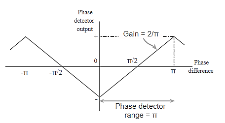
Fig 18 EX-OR Phase Detector Response Curve
- The nominal lock point with an XOR phase detector is also at the 90° static phase shift point.
Unlike an analogue mixer phase detector, the XOR version is independent of input amplitude and constant over a π phase range.
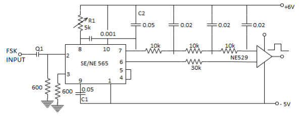
Fig 19 IC 565 PLL
A PLL may be used to demodulate AM signals as shown in the figure below. The PLL is locked to the carrier frequency of the incoming AM signal. The output of VCO which has the same frequency as the carrier, but unmodulated is fed to the multiplier.
Since VCO output is always 900 before being fed to the multiplier. This makes both the signals applied to the multiplier and the difference signals, the demodulated output is obtained after filtering high frequency components by the LPF.
Since the PLL responds only to the carrier frequencies which are very close to the VCO output, a PLL AM detector exhibits high degree of selectivity and noise immunity which is not possible with conventional peak detector type AM modulators.
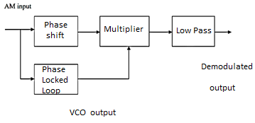
Fig 20 AM Demodulation
FM Demodulation:
If PLL is locked to a FM signal, the VCO tracks the instantaneous frequency of the input signal. The filtered error voltage which controls the VCO and maintains lock with the input signal is the demodulated FM output. The VCO transfer characteristics determine the linearity of the demodulated output.
Since, VCO used in IC PLL is highly linear, it is possible to realize highly linear FM demodulators.
Application
The PLL is widely used in frequency synthesis to generate spectrally pure signals and, if necessary, to operate as an analog or digital frequency or phase modulator.
Frequency multiplication or division, frequency addition or subtraction may be performed, using a PLL in conjunction with programmable frequency dividers and mixers as shown in Fig.
As a result, the output frequency fo depends on the reference fR and offset fS frequencies, moreover, on the division ratios of frequency dividers. In frequency synthesis, the PLL input is called reference signal and its frequency is denoted by fR.
To optimize the system performance, frequently a multiloop circuit configuration is used.
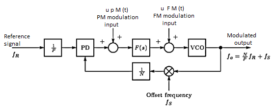
Fig 21 Frequency Synthesis
In frequency synthesis, the dominant noise sources are the VCO, frequency dividers, mixers, and phase detectors.
The main design goals are to minimize the output phase noise, to avoid the generation of spurious output signals, and to minimize the unwanted output FM caused by the periodic output of the phase detector.
These requirements can be satisfied with special PD configurations, such as sample-and-hold phase detector or phase-frequency detector with a charge-pump circuit.
In addition to frequency synthesis, PLLs may be also used as FM or PM modulators.
The corresponding transfer functions for FM and PM are
sΘo(s) = [1 − H(s)]KvVFM(s)
Θo(s) = H(s) N AK VPM(s) (3)
Where Kv and N/(AK) are the gains of the FM and PM modulators, respectively.
H(s) and [1 − H(s)] denote the closed-loop transfer and error functions, respectively.
However, since the frequency synthesizer has a frequency divider in the feedback path, the loop gain becomes
K = KgKdKv
Key takeaway
In addition to frequency synthesis, PLLs may be also used as FM or PM modulators. A PLL may be used to demodulate AM signals.
Solved Examples
Q1) For the multivibrator in Fig. Below, R1 = R2 = R = 47 k , C1 = C2 = C = 0.01 μF. Find the time period and frequency.
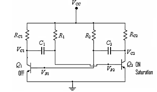
Sol: Given R1 = R2 = R = 47 k ,C1 = C2 = 0.01 µF. This is a symmetric astable multivibrator.
T=1.38 RC= 1.38 x 47x 1000x 0.01 x 10-6= 0.648ms
F=1/T = 1/0.648ms = 1.54kHz
Q2) For the astable multivibrator in Fig. In Q1, R1 = 20 k , R2 = 30 k ,C1 = C2 = C = 0.01 μF. Find the time period, duty cycle and the frequency.
Sol:
This is an un-symmetric astable multivibrator.


Per cent 

Q3) For the symmetric astable multivibrator that generates square waves with vertical edges shown in Fig.7p.3, VCC=10 V, RC = R3= 2 k , R1 = R2 = 20 k , C = 0.1 F, hFE(min) = 30. Show that the ON device is in saturation. Also find f. Assume suitable values for VCE(sat) and VBE(sat). Si transistors are used.
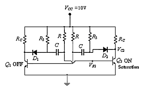
Sol: Assume Q1 is OFF and Q2 is ON and in saturation. If Q2 is ON and in saturation, for silicon transistors, VC2 =VCE(sat) = 0.2 V, VB2 = Vσ = 0.7 V then D2 is ON. The collector load is R3//RC.


 =0.465mA

IB2 >> IB2min
Hence Q2 is in saturation.
To find f: For a symmetric astable multivibrator:

Q4) Design a symmetric collector-coupled astable multivibrator to generate a square wave of 10 kHz having peak-to-peak amplitude of 10 V where hFEmin = 30, VCE(sat) = 0.2 V, IC(sat) = 2 mA.
Sol:

As the output amplitude is specified as 12V, choose 
As 

The astable is symmetric, hence
 and
and 

To calculate 


To calculate 


If  is in saturation


As 


Q5) Design an un-symmetric astable multivibrator having duty cycle of 40 per cent. It is required to oscillate at 5 kHz. Ge transistors with hFE = 40 are used. The amplitude of the square wave is required to be 20 V. IC = 5 mA, VCE(sat) = 0.1 V and VBE(sat) = 0.3 V
Sol:
For Ge transistors, VCE(sat) = 0.1 V, VBE(sat) = V = 0.3 V
IC(sat) = 5 mA, f = 5 kHz, hFEmin = 40, duty cycle = 40 per cent. As the output amplitude is specified as 20 V, choose VCC = 20 V. As f = 5 kHz,
T= 1/f = 1/5x1000= 0.2ms
The astable is unsymmetric, hence


Choose 
Then 
Duty cycle 


To calculate 


Choose 
To calculate 


If  is in saturation


As 


The values R1 and R2 are less than hFERC. Hence the devices Q1 and Q2 are in saturation, when ON.
Q6) For an un-symmetric astable multivibratorR1 = 100 kΩ, R2 = 100 kΩ, C1 = 0.02 F, C2 = 0.01F. Find the frequency of oscillation and the duty cycle.
Sol:


% D = T1/T x 100 % = [0.69/2.09 x 10-3] x 100 % = 33%
Q7) Design an unsymmetrical astable multivibrator shown in Figure using silicon n– p–n transistors having an output amplitude of 12 V. Given data, IC(sat) = 5 mA, hFEmin = 50, f = 5 kHz, duty cycle = 0.6.
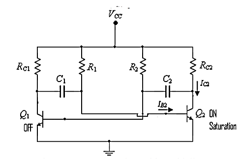
Sol: Assume VCE(sat) = 0.2 V, VBE(sat) = V = 0.7 V
Given IC(sat) = 5 mA, f = 2 kHz, hFEmin = 50, duty cycle = 0.6. As the output amplitude is specified as 12 V, choose VCC = 12 V. As f = 2 kHz,

The stable is unsymmetric, hence


Choose 
Then 
Duty cycle 


To calculate 


Choose 
To calculate 


If  is in saturation


As 


The values R1 and R2 are less than hFERC. Hence the devices Q1 and Q2 are in saturation, when ON.
Q8) A Voltage-to-frequency converter shown in Figure generates oscillations at a frequency f1 when VBB = VCC. Find the ratio of VCC /VBB at which the frequency f2 = 4f1.
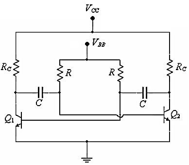
Sol:

Case1: The frequency of oscillations is f1 when VCC = VBB

Case 2: If a new frequency f2 = 4f1 is desired.


Taking antilog


References:
1. Gayakwad: Op-Amps and Linear Integrated Circuits, 4th Edition Prentice Hall of India, 2002.
2. Franco, Analog Circuit Design: Discrete & Integrated, TMH, 1st Edition.
3. Salivahnan, Electronics Devices and Circuits, TMH, 3rd Edition, 2015
4. Millman and Halkias: Integrated Electronics, TMH, 2nd Edition, 2010