Unit – 1
Introduction to Microprocessor
It includes the timing & control unit, Arithmetic and logic unit, decoder, instruction register, interrupt control, a register array, serial input/output control and the central processing unit.
Operations of 8085 Microprocessor
It performs all arithmetical and logical operations like add, subtract, AND, OR etc. The temporary registers and accumulators hold the information throughout the operations and the result is stored in the accumulator. The different flags are arranged or rearranged on the basis of result.
Control and Timing Unit
It coordinates with all the processes of the microprocessor by the clock and provides the control signals required for communication between the microprocessor and peripherals. It is used to control the internal as well as external circuits.
Decoder and Instruction Register, when an order is received from memory which is located in the instruction register, it is encoded & decoded into various device cycles.
- Special Purpose Registers
These registers are of four types namely program counter, stack pointer, increment or decrement register, address or data buffer.
Program Counter
It is a 16-bit register. It is used to store data, memory information etc. whenever memory is incremented, the PC then points to the next location.
Stack Pointer
It is a 16-bit register. It always points to stack which can be incremented or decremented by PUSH and POP instruction.
Increment or Decrement Register
It is an 8-bit register which can be increased or decreased by one. It is useful for incrementing or decrementing program counters as well as stack pointer register content with one. This operation can be done on any memory location or any kind of register.
Address Bus and Data Bus
Data bus carries the data required to be stored. It is bidirectional. Address bus carries the location to where the data should be stored and it is unidirectional. It is used to transfer the data & address.
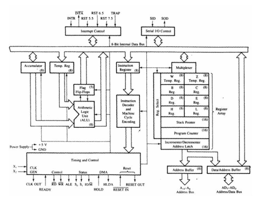
Fig.1: Architecture of 8085 (ref 1)
Key takeaway
It includes the timing & control unit, Arithmetic and logic unit, decoder, instruction register, interrupt control, a register array, serial input/output control and the central processing unit.
Memory is the location where information is kept while not in current use. Memory is a collection of storage devices. Usually, each storage device holds one bit. Also, in most kinds of memory, these storage devices are grouped into groups of 8. These 8 storage locations can only be accessed together. So, one can only read or write in terms of bytes to and from memory.
Memory is usually measured by the number of bytes it can hold. It is measured in Kilos, Megas and lately Gigas. A Kilo in computer language is 210 =1024. So, a KB (Kilobyte) is 1024 bytes. Mega is 1024 Kilos and Giga is 1024 Mega. When a program is entered into a computer, it is stored in memory. Then as the microprocessor starts to execute the instructions, it brings the instructions from memory one at a time.
Memory is also used to hold the data. The microprocessor reads (brings in) the data from memory when it needs it and writes (stores) the results into memory when it is done.
The Input Output devices gets connected to a computer through the Input Output ports. Two Instructions are fetched which are called as IN and OUT where there are 256 Input Ports and 256 Output ports. For the communication with a printer, the CPU loads the output port connected to the printer which works at electronic speeds. The printer prints the total information at about 15-20 s.
I/O port chip with a single port is shown below.
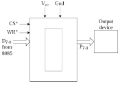
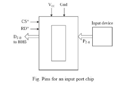
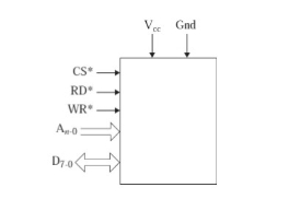
In 8085 Instruction set, there are two instructions in 8085 for communication with I/O ports. They are the IN and OUT instructions. The IN or OUT instruction mnemonic should be followed by an 8-bit port address. Thus, we can have 2 8 = 256 input ports and 256 output ports are possible in 8085-based microcomputer. IN and OUT both are 2-Byte’s instructions.
Mnemonics, Operand | Opcode (in HEX) | Bytes |
IN Port-address | DB | 2 |
OUT Port-Address | D3 | 2 |
In case of IN instruction, the current 8-bit content of the PORT# will be made available on to the Accumulator.
Let us suppose with the PORT#, 8 DIP switches are connected. And their states are ON-ON-OFF-ON-ON-ON-OFF-ON. So, after execution of the instruction IN PORT#, the Accumulator content will be 1101 1101.
In case of OUT instruction, the current 8-bit content of the Accumulator will be copied on to the PORT#. Let us suppose that Accumulator’s initial content is 0101 0101. And with the 8-bit port 8 LEDs are connected. So, after execution of the instruction OUT PORT#, LEDs will have the states as shown.

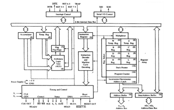
8085 consists of the following functional units −
Accumulator
The accumulator is an 8-bit register used to perform arithmetic, logical, I/O & LOAD/STORE operations. It is connected to internal data bus & ALU.
Arithmetic and logic unit
The arithmetic and logic unit performs arithmetic and logical operations like Addition, Subtraction, AND, OR, etc. on 8-bit data.
General purpose register
8085 consists of six general purpose registers in 8085 processor that is B, C, D, E, H & L. Each register holds 8-bit data. These registers work in pair to hold 16-bit data and their pairing combination is like B-C, D-E & H-L.
Program counter
It is a 16-bit register used to store the memory address location of the next instruction to be executed. Microprocessor increments the program whenever an instruction is being executed, so that the program counter points to the memory address of the next instruction that is going to be executed.
Stack pointer
It is 16-bit register which works like stack, which gets incremented/decremented by 2 during push & pop operations.
Temporary register
It is an 8-bit register, which holds the temporary data of arithmetic and logical operations.
Flag register
It is an 8-bit register which holds 0 or 1 depending upon the result stored in the accumulator.
These are:
- Sign (S)
- Zero (Z)
- Auxiliary Carry (AC)
- Parity (P)
- Carry (C)

Instruction registers and decoder
It is an 8-bit register. When an instruction is fetched from memory then it is stored in the Instruction register. Instruction decoder decodes the information present in the Instruction register.
Timing and control unit
It provides timing and control signal to the microprocessor to perform operations. Following are the timing and control signals, which control external and internal circuits −
- Control Signals: READY, RD’, WR’, ALE
- Status Signals: S0, S1, IO/M’
- DMA Signals: HOLD, HLDA
- RESET Signals: RESET IN, RESET OUT
Interrupt control
It controls the interrupts during the process. When the microprocessor is executing the main program and whenever an interrupt occurs, the microprocessor shifts the control from the main program to process the incoming request. After the request is completed, the control returns to the main program.
There are 5 interrupt signals in 8085 microprocessors:
- INTR
- RST 7.5
- RST 6.5
- RST 5.5
- TRAP.
Serial Input/output control
It controls the serial data communication by using the two instructions: SID (Serial input data) and SOD (Serial output data).
Address buffer and address-data buffer
The content stored in the stack pointer and program counter is loaded into the address buffer and address-data buffer to communicate with the CPU.
The memory and I/O chips are connected to these buses, the CPU can exchange the desired data with the memory and I/O chips.
Address bus and data bus
Data bus carries the data to be stored. It is bidirectional whereas address bus carries the location to where it should be stored, and it is unidirectional. It is used to transfer the data & Address I/O devices.
Pin Diagram of 8085
The 40 pins of microprocessor can be divided into six groups such as
Address bus
Data bus
Control signals & status signals
Power supply & frequency
Externally started signals
Serial input/output ports.
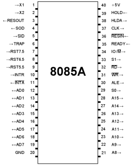
8085 Microprocessor pin Configuration
Address Bus (A8-A15)
The address bus pins A8 to A15 are applicable to the most considerable memory address bit.
Address Bus (or) Data Bus (AD0-AD7)
The address bus pins or data bus pins ranges from AD0 to AD7, and these pins are applicable for LSB (least significant bits) of the address bus in the primary apparatus CLK cycle as well as employed as a data bus for second clock cycle & third clock cycle.
A CLK cycle is designed as time in use among two oscillator’s nearby pulses, or simply it can refer to zero volts. Here the first clock is the primary transition of pulse ranges from 0V to 5V & then reaches back to 0V.
Address Latch Enable (ALE)
ALE (Address Enable Latch) is the control signal a positive going pulse generated when a new operation is started by microprocessor. So, when pulse goes high means ALE=1, it makes address bus enable and when ALE=0, means low pulse makes data bus enable.
Status Signal (IO/M)
The status signal IO/M resolves whether the address is intended for memory or input/output. When the address is high then the address of the address bus is used for the devices of input/output devices. When the address is low then the address of the address bus is used for the memory.
Status Signals (S0-S1)
The status signals S0, S1 gives different functions as well as status based on their status.
- When the S0, S1 are 01 then the operation will be HALT.
- The S0, S1 is 10 then the operation will be WRITE
- When the S0, S1 is 10 then the operation will be READ
- When the S0, S1 are 11 then the operation will be FETCH
Active Low Signal (RD)
This signal indicates that the selected IO or memory device is to be read and is ready for accepting data available on the data bus.
Active low signal WR
This signal indicates that the data on the data bus is to be written into a selected memory or IO location.
READY
The READY pin is employed for ensuring whether a device is set for accepting or transferring data.
A device may be an A/D converter or LCD display, etc. These devices are associated with the 8085 microprocessors with the READY pin.
When this pin is high, the device is prepared for transferring the information, if it is not then the microprocessor stays until this pin goes high.
HOLD
The signal indicates that another master is requesting the use of address and data buses.
HLDA (Hold Acknowledge)
This signal indicates that CPU has received the HOLD request and it will relinquish the bus in the next clock cycle. HLDA is set to low after HOLD signal is removed.
INTR
This is an interrupt signal, and the priority of this among the interrupt is low. This signal can be allowed or not allowed by the software. When INTR pin goes high then the 8085 microprocessor completes the instruction of current which is being executed and then recognizes the INTR signal and progresses it.
INTA
When the 8085 microprocessor gets an interrupt signal, then it should be recognized. This will be done by INTA. As a result, when the interrupt will be obtained then INTA will go high.
RST 5.5, RST 6.5, RST 7.5
These pins are the restart maskable interrupts or Vectored Interrupts, used to insert an inner restart function repeatedly. All these interrupts are maskable, they can be allowed or not allowed by using programs.
TRAP
Along with the 8085 microprocessor interrupts, TRAP is a non-maskable interrupt, and it doesn’t allow or stopped by a program. TRAP has the maximum precedence between the interrupts. The priority order from maximum to low includes TRAP, RST 5.5, RST 6.5, RST 7.5, and INTR.
RESET IN
RESET IN pin is used to reset the program counter toward zero and rearranges interrupt enable as well as HLDA flip flops (FFs). The central processing unit is detained in RST condition till this pin is high. But the registers as well as flags won’t get damaged apart from instruction register.
RST (RESET) OUT
RESET OUT pin specifies that the central processing unit has been rearranged with RST IN.
X1 X2
X1, X2 terminals that are associated with the exterior oscillator for generating the required as well as appropriate operation of a clock.
CLK
Sometimes it is compulsory to generate CLK o/PS from 8085 microprocessors so they can be used in favour of other peripherals or else other digital integrated circuits. This is offered with CLK pin. Its frequency is continually similar because the frequency at which the microprocessor works.
SID
This is a serial i/p data, and the information on this pin is uploaded into the 7th-bit of the accumulator while RIM (Read Interrupt Mask) instruction is performed. RIM verifies the interrupt whether it is covered or not covered.
SOD
This is the serial o/p data, and the data on this pin sends its output toward the 7th-bit of the accumulator whenever an instruction of SIM is performed.
VSS and VCC
VSS is a ground pin whereas Vcc is +5v pin.
- Timing diagram helps to understand the working of any system step by step and working of each instruction, its decoding, fetching and execution.
- It is the graphical representation with respect to time.
- It represents the clock cycle with duration, delay, content of address bus and data bus, type of operation w.r.to Read/write/status signals.
Important terms used
1. Instruction cycle: It is defined as the number of steps required by the CPU to complete the process which includes fetching, decoding and execution of one instruction. They are carried out in synchronization with the clock pulse.
2. Machine cycle: It is the time required by the microprocessor to complete the operation of accessing the memory or I/O devices. Here, operations like opcode fetch, memory read, memory write, I/O read and I/O write can be performed.
3. T-state: Each clock cycle is known as T-state.
Rules to identify number of machine cycles in an instruction:
1. If an addressing mode is direct, immediate or implicit then
No. Of machine cycles = No. Of bytes.
2. If the addressing mode is indirect then
No. Of machine cycles = No. Of bytes + 1.
Add +1 to the No. Of machine cycles if it is memory read/write operation.
3. If the operand is 8-bit or 16-bit address then,
No. Of machine cycles = No. Of bytes +1.
4. These rules are applicable to 80% of the instructions of 8085.

Fig.: Timing Diagram
Fetch cycle
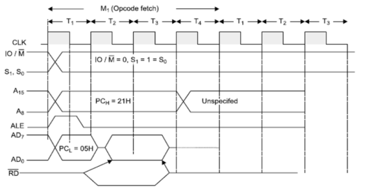
Fetch Cycle
- The microprocessor requires instructions to perform any particular task. In order to perform these tasks, it utilizes Opcode which is a part of an instruction which provides detail to the microprocessor.
During T1 state, microprocessor uses IO/M, S0, S1 signals are used to instruct microprocessor to fetch opcode.
Thus, when IO/M =0 and S0=S1= 1, it indicates opcode fetch operation.
During this operation 8085 transmits 16-bit address and also uses ALE signal for address latching.
At T2 state, microprocessor uses read signal and make data ready from that memory location to read opcode from memory and at the same time program counter is incremented by 1 and points next instruction to be fetched.
In this state microprocessor also checks READY input signal, if this pin is at low logic level i.e., '0' then microprocessor adds wait state immediately between T2 and T3.
At T3 state, microprocessor reads the opcode and stores it into instruction register to decode it further.
At T4 state, the microprocessor performs internal operation like decoding opcode and providing necessary actions.
The opcode is decoded to know whether T5 or T6 states are required or not for next operation.
Read Cycle
1. Memory read
2. I/O read
Memory Read
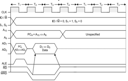
Memory read Cycle
It fetches one byte from the memory at a time.
It requires 3 T-States.
It is used to fetch operand or data from the memory.
 During T1 state, A8-A15 contains higher byte of address, ALE is high therefore lower byte of address A0-A7 is selected from the multiplexed lines AD0-AD7.
Since it is a memory ready operation, IO/M =0.
 During T2state, ALE = 0, RD = 0 and address is removed from AD0-AD7 and data D0-D7 appears on the lines AD0-AD7.
 During T3 state, data remains on AD0-AD7 till, RD = 0.
I/O Read
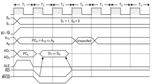
I/O read Cycle


 It is used to fetch one byte from an IO port at a time.
It requires 3 T-States.
During T1 state, the lower Byte of IO address is copied into higher order address bus A8-A15.
ALE = 1 and AD0-AD7 contains address of IO device.
IO/M = 1 as it is an IO operation.
During T2 state, ALE = 0, RD = 0 and data appears on AD0-AD7 as input from IO device.
During T3 state, data remains on AD0-AD7 till RD = 0.
Write Cycle
1. Memory write
2. I/O write
Memory write cycle
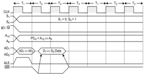
Memory write Cycle
It is used to send one byte at a time into memory.
It requires 3 T-States.
During T1 state, ALE = 1 and contains lower address A0-A7 from multiplexed lines AD0-AD7 and A8-A15 contains higher byte of address.

 As it is memory operation, IO/M = 0.
 During T2 state, ALE = 0, WR = 0 and address is removed from AD0-AD7 and data appears on AD0-AD7.
Data remains on AD0-AD7 till WR = 0.
I/O write cycle
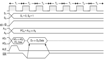
I/O write Cycle
It is used to write one byte at a time into IO device.
It requires 3 T-States.
During T1 state, the lower byte of address is copied into higher order address bus A8-A15.
ALE =1 and A0-A7 address is selected from the multiplied lines AD0-AD7.
 As it is an IO operation, IO/M = 1.
 During T2 state, ALE = 0, WR = 0 and data appears on AD0-AD7 to write data into IO device.
 During T3 state, data remains on AD0-AD7 till WR = 0.
These logic devices play an important role in 8085 microprocessor. To separate the low order address bus and data bus, latch IC is used. A tri-state logic device has an extra input line called Enable. When this line is active (Enabled), a tri-state device functions in the same way as ordinary logic devices. An interface device (IDF) is a hardware component or system of components that allows a human being to interact with a computer, a telephone system, or other electronic information system.
LOGIC DEVICES FOR INTERFACING
Tri-State devices
Buffer
Bidirectional Buffer
Decoder
Encoder
D Flip Flop: Latch and Clock
TRI-STATE LOGIC OUTPUTS:
Since we can have multiple masters on a bus, we need Tri-state logic for attachment to a bus so that each device can choose to drive or not drive the bus depending on whether it is the bus master for a given bus cycle.
Tri-state logic prevents a bus conflict where one device is driving a signal to 1 and another device is driving it to 0 at the same time - generates high current through wires.
TRI-STATE LOGIC AND BUSES
The logical element has output enable pin to go from a floating output to drive the output from the circuit
Inverters and buffers are used as bus drivers or buffers
Two such drivers or buffers in opposite directions are used to make the connection bi-directional
The gates also provide more “drive” onto the bus so that the bus signals are stronger and the bus can be longer

The problem with connecting multiple “normal” outputs together on a bus is that each has to be in one logic state (0) or the other (1) - driving voltage on each bus signal high or low.
This represents a conflict over the state of the signal.
We resolve this conflict with tri-state logic.

Buses:
Concept is to link together multiple functional units over a common data highway at a lower cost than using multiple point to point links.
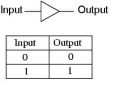
Buffer:
A buffer has only a single input and a single output with behaviour that is the opposite of an NOT gate. It simply passes its input, unchanged, to its output. In a Boolean logic simulator, a buffer is mainly used to increase propagation delay. In a real-world circuit, a buffer can be used to amplify a signal if its current is too weak.
DECODER
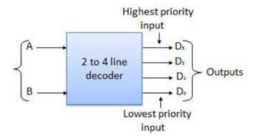
A decoder is a device which does the reverse operation of an encoder, undoing the encoding so that the original information can be retrieved. The same method used to encode is usually just reversed in order to decode. It is a combinational circuit that converts binary information from n input lines to a maximum of 2n unique output lines.
ENCODER
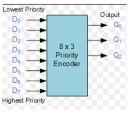
An encoder is a device, circuit, transducer, software program, algorithm or person that converts information from one format or code to another, for the purposes of standardization, speed, secrecy, security or compressions.
FLIP FLOP
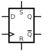
A flip-flop or latch is a circuit that has two stable states and can be used to store state information. A flip-flop is a bistable multivibrator. The circuit can be made to change state by signals applied to one or more control inputs and will have one or two outputs.
The D flip-flop is widely used. It is also known as a "data" or "delay" flip-flop.
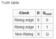
The D flip-flop captures the value of the D-input at a definite portion of the clock cycle (such as the rising edge of the clock). That captured value becomes the Q output. At other times, the output Q does not change. The D flip-flop can be viewed as a memory cell, a zero-order hold, or a delay line.
Memory is an integral part of a microprocessor system, and in this section, we will discuss how to interface a memory device with the microprocessor. The Memory Interfacing in 8085 is used to access memory quite frequently to read instruction codes and data stored in memory. This read/write operations are monitored by control signals. The microprocessor activates these signals when it wants to read from and write into memory.
The read/write memories consist of an array of registers, in which each register has unique address. The size of the memory is N x M as shown in Fig. (a) where N is the number of registers and M is the word length, in number of bits.
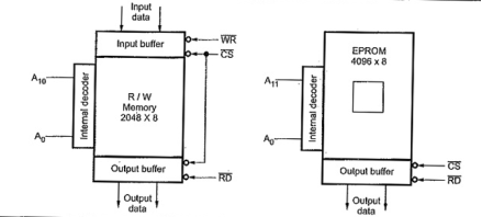
(a) Logic diagram for RAM (b) Logic diagram for EPROM
- Microprocessor 8085 can access 64Kbytes memory since address bus is 16-bit. But it is not always necessary to use full 64Kbytes address space. The total memory size depends upon the application.
- Generally, EPROM (or EPROMs) is used as a program memory and RAM (or RAMs) as a data memory. When both, EPROM and RAM are used, the total address space 64Kbytes is shared by them.
- The capacity of program memory and data memory depends on the application.
- It is not always necessary to select 1 EPROM and 1 RAM. We can have multiple EPROMs and multiple RAMs as per the requirement of application.
- We can place EPROM/RAM anywhere in full 64 Kbytes address space. But program memory (EPROM) should be located from address 0000H since reset address of 8085 microprocessor is 0000H.
- It is not always necessary to locate EPROM and RAM in consecutive memory. For example: If the mapping of EPROM is from 0000H to OFFFH, it is not must to locate RAM from 1000H. We can locate it anywhere between 1000H and FFFFH. Where to locate memory component totally depends on the application.
The memory interfacing requires to:
Select the chip
Identify the register
Enable the appropriate buffer.
Microprocessor system includes memory devices and I/O devices. It is important to note that microprocessor can communicate (read/write) with only one device at a time, since the data, address and control buses are common for all the devices. In order to communicate with memory or I/O devices, it is necessary to decode the address from the microprocessor. Due to this each device (memory or I/O) can be accessed independently.
The microprocessor 8085 sends 8-bit data to the output device such as 7 segment displays, LEDs, printer etc. Figure shows the circuit diagram to interface output port (latch) which is used to send the signal for glowing the LEDs. LED will glow when output pin status is low. The IC 74LS138 and 3 input OR gate is used to generate device select signal. The latch enable signal is active high. So, NOR gate is used to generate latch enable signal, which goes high when Y1 and IOW both are low.
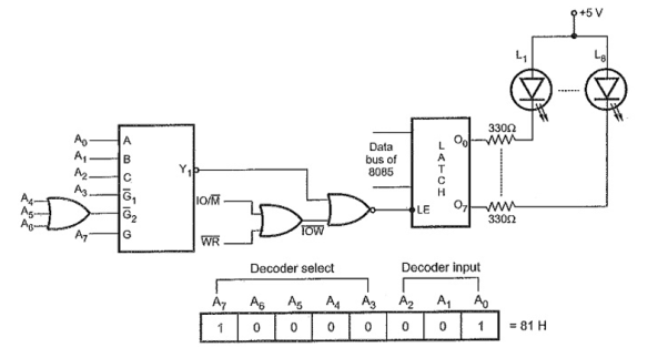
Figure. Circuit diagram to interface output port.
The microprocessor 8085 accepts 8-bit data from the input device such as keyboard, sensors, transducers etc. Figure shows the circuit diagram to Input Output Interfacing Techniques (buffer) which is used to read the status of 8 switches. The address for this input device is 80H as device select signal goes low when address is 80H.
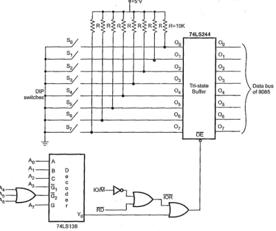
Figure. Interface input port
In memory mapped I/O, the I/O devices are assigned and identified by 16-bit addresses. The memory related instructions transfer the data between an I/O device and the microprocessor, as long as I/O port is assigned to the memory address space rather than to the I/O address space. The register associated with the I/O port is simply treated as a memory location. Thus I/O device becomes a part of the system’s memory map and hence its name.
In memory-mapped I/O every instruction that refers to a memory location can control I/O. The source and destination of the data is limited with I/O mapped I/O, since for an IN instruction the destination register is always the accumulator, and for the OUT instruction the source register is always the accumulator. However, for memory mapped I/O there are number of sources and destinations.
Interfacing of I/O port with memory mapped I/O:
In memory mapped I/O, MEMR (memory read) and MEMW (memory write) control signals are required to control the data transfer between I/O device and microprocessor. As 8085 gives 16-bit memory address, it is necessary to decode 16-bit memory address to generate device select signal in case of memory mapped I/O. Fig. Shows the Input Output Interfacing Techniques devices in memory mapped I/O mode.
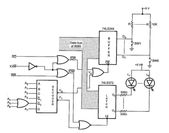
Figure: I/O interfacing using I/O Mapped I/O
References:
1. Microprocessor Architecture, Programming, and ...Book by Ramesh S. Gaonkar
2. 8085 Microprocessor: Programming and Interfacing Book by N. K. Srinath
3. 8085 Microprocessors & Its Application Book by Nagoorkani