Unit – 4
8051 Microcontroller Basics
A microcontroller is seen as a small computer because of the essential components inside of it; the Central Processing Unit (CPU), the Random-Access Memory (RAM), the Flash Memory, the Serial Bus Interface, the Input/Output Ports (I/O Ports), and in many cases, the Electrical Erasable Programmable Read-Only Memory (EEPROM). Figure shows the main parts and also other parts in the microcontroller.
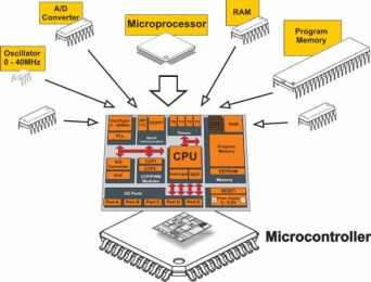
Figure: Parts of a microcontroller.
Design of Microcontroller CPU
The CPU sometimes called a processor or microprocessor, controls all of the instructions/data flow that it receives. You can think of it as the brains of the system, processing all the data input it receives and executes the required instructions. Its two main components are the Arithmetic Logic Unit (ALU), which performs arithmetic and logical operations, and the Control Unit (CU), which handles all of the processor’s instruction executions. Figure shows a usual "machine cycle" that the CPU goes through.
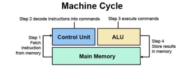
Figure. A typical machine cycle that the CPU executes.
Microcontroller RAM
RAM is a component that temporarily stores data, and can be accessed quickly. It provides quick read-and-write access to the storage device. This differs from most other memories as it takes longer for data to be extracted since the data isn’t readily available. You can see it as RAM having access to the surface of data – easily reachable – but anything that dives deeper will require a different type of memory. RAM improves total system performance because it allows the microcontroller to work with more information at the same time. Since RAM is temporary data, its content is always erased when the microcontroller is shut down.
Use of Flash Memory in Microcontrollers
Flash memory is a type of non-volatile memory that, unlike RAM, retains its data for an extended period, even if the microcontroller is turned off. This keeps the saved program that you might have uploaded to the microcontroller. Flash Memory writes to a “block” or “sector” at a time, so if you need to just re-write one byte, Flash Memory will need to re-write the whole block that the byte is in, which can wear out quicker.
EEPROM
EEPROM is like Flash Memory, being a non-volatile memory and retaining its data even after shutdown. The difference is that, while Flash Memory re-writes a “block” of bytes, EEPROM can re-write any specific byte at any time. This extends the life of EEPROM compared to Flash Memory, but also means that it is more expensive.
Serial Bus Interface
A Serial Bus Interface is the serial communication in the microcontroller, sending data one bit at a time. With microcontroller boards, it connects ICs with signal traces on a printed circuit board (PCB). For ICs, they use serial bus to transfer data to reduce the number of pins in a package making them more cost effective. Examples of serial buses in ICs are SPIs or I2Cs.
Microcontroller I/O Ports
I/O ports are what the microcontroller uses to connect to real-world applications. Inputs receive changes in the real-world, from temperature sensing, to motion sensing, to push buttons, and much more. The input then goes to the CPU and decides what to do with that information. When it’s time to do a certain command based on a certain value from the input, it sends a signal to the output ports, where it can range from a simple LED light going off, to running a motor for a certain part, to many more. Figure shows some common input and output components.
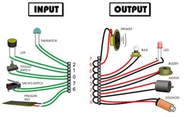
Figure. Common inputs and output components that are used for microcontroller.
An embedded processor is a type of microprocessor which is designed into a system to control electrical and mechanical functions. Embedded processors are simple in design, limited in computational power and I/O capabilities, and have minimal power requirements. At a basic level, embedded processors are a CPU chip placed in a system that it helps control.
Embedded processors are often confused with microcontrollers. While they do perform similar functions, they integrate with their given system in different ways. The actual functions they perform can also be different as well.
Microcontrollers are the result of technological advances decreasing the size of controllers. Eventually, all of the components of a controller including I/O devices and memory evolved into a single chip, giving us the “micro” in microcontrollers. These chips are small, self-contained devices that have all of the features necessary to control the system they are embedded in.
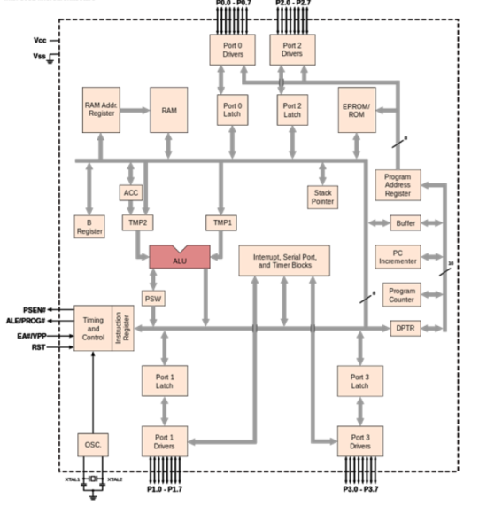
Figure. 8051 internal block diagrams
It is an 8-bit microcontroller. It is built with 40 pins DIP (dual inline package), 4kb of ROM storage and 128 bytes of RAM storage, 2 16-bit timers. It consists of are four parallel 8-bit ports, which are programmable as well as addressable as per the requirement.
The reasons for the popularity of 8051 Microcontroller are –
- Simple to integrate in any electronic device.
- Affordable.
- Simple architecture.
- Easy instruction set.
- Low computing power.
CPU
The CPU act as a mind of any processing machine. It synchronizes and manages all processes that are carried out in microcontroller. The user has no power to control the functioning of CPU. It interprets the program stored in ROM and carries out from storage and then performs it projected duty. CPU manage the different types of registers available in 8051 microcontrollers.
It is the heart of the Microcontroller that mainly comprises of an Arithmetic Logic Unit (ALU) and a Control Unit (CU) and other important components. The CPU is the primary device in communicating with peripheral devices like Memory, Input and Output.
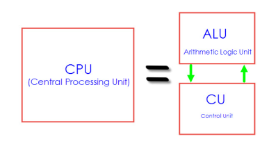
Figure. CPU
ALU
ALU performs all arithmetic and logical functions.
Addition, subtraction with carry, and multiplication are categorized as arithmetic operations.
Logical AND, OR and exclusive OR (XOR) as logical operations.
Address, Data Bus and Control Bus
A bus consists of group of wires to transfer data from one location to another within the system. Buses reduce the number of paths or cables needed to set up connection between component.
There are two kinds of buses - Data Bus and Address Bus
Data Bus: The purpose of data bus is to transfer data. It acts as a channel for data to travel.
Address Bus: The purpose of address bus is to transfer information but not data. The information tells from where within the components, the data should be sent to or received from.
Control bus - carries control signals from the processor to other components. The control bus also carries the clock's pulses. The control bus is unidirectional
Working Registers
Registers are known as data storage devices. There are two registers namely Register A and Register B. Register A is used as an accumulator and Register B as general -purpose register. The output of mathematical and logical instructions is stored in these registers.
The operations of addition, subtraction, multiplication and division are performed by Register A. Register B is for multiplication and division which are carried by Register A. For data transfers between microcontroller and external memory Register A is involved.
8051 has four Register banks.
When the 8051 is first booted up Register bank 0 (addresses 00h through 07h) is used by default.
The internal memory supports 4 register banks.
The first 8 bytes (00h – 07h) are “register bank 0”.
Followed by Bank1 (08 – 0F),
Bank2 (10 – 17),
Bank3 (18 – 1F).
Register banks reside in the first 32 bytes of Internal RAM.
PSW (PROGRAM STATUS WORD)
This is an 8-BIT register. The Program Status Word (PSW) contains status bits that reflect the current CPU state.
A (ACCUMULATOR)
Accumulator is an 8-bit register. It holds the result of most of arithmetic and logic operations. This register is usually accessed by direct addressing. It is both byte and bit addressable.
B (EXTENSION REGISTER)
The major purpose of B (Extension register) register is executing multiplication and division. This register is directly accessed when we are writing our code in assembly language. The 8051 micro controller has a single instruction for multiplication (MUL) and division (DIV).
SP (STACK POINTER)
Stack pointer is an 8- bit register, the direct address of SP is 81H and it is only byte addressable that means individual bits of stack pointer cannot be accessed. The content of the stack pointer points to the last stored location of system stack.
To store something new in system stack, the SP must be incremented by 1 first and then execute the “store” command.
- Push increments the SP and writes data.
- POP reads data and then decrements the SP.
- Stack is kept in the internal RAM and is restricted to 128 bytes.
- Top most address of stack is 7F.
DPTR (DATA POINTER REGISTER)
This is a 16-bit register. It is used to access external code or data memory
The Data Pointer (DPTR) is the 8051’s only user-accessible 16-bit (2-byte) register.
PSW (program status word) register: The program status word (PSW) register is an 8-bit register. It is also referred to as the flag register. Although the PSW register is 8 bits wide, only 6 bits of it are used by the 8051. The two unused bits are user-definable flags.
Four of the flags are called conditional flags, meaning that they indicate some conditions that result after an instruction is executed. These four are CY (carry), AC (auxiliary carry), P (parity), and OV (overflow).
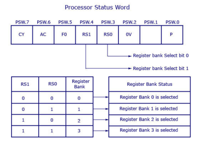
The bits PSW.3 and PSW.4 are designated as RSO and RSI, respectively, and are used to change the bank registers. The PSW.5 and PSW.l bits are general-purpose status flag bits and can be used by the programmer for any purpose.

CY | PSW.7 | Carry flag |
AC | PSW.6 | Auxiliary carry flag |
F0 | PSW.5 | Available to user for general purpose |
RS1 | PSW.4 | Register Bank selector bit 1 |
RS0 | PSW.3 | Register Bank selector bit 0 |
OV | PSW.2 | Overflow flag |
--- | PSW.1 | User-definable bit |
P | PSW.0 | Parity flag Set/Cleared by hardware each instruction cycle to indicate an odd/even number of bits in the accumulator. |
RS1 | RS2 | Register Bank | Address |
0 | 0 | 0 | 00H – 07H |
0 | 1 | 1 | 08H-0FH |
1 | 0 | 2 | 10H-17H |
1 | 1 | 3 | 18H-1FH |
● CY, the carry flag
This flag is set whenever there is a carry out from the D7 bit. This flag bit is affected after an 8-bit addition or subtraction. It can also be set to 1 or 0 directly by an instruction such as “SETB C” and “CLR C” where “SETB C” stands for “set bit carry” and “CLR C” for “clear carry”.
● AC, the auxiliary carry flag
If there is a carry from D3 to D4 during an ADD or SUB operation, this bit is set; otherwise, it is cleared. This flag is used by instructions that perform BCD (binary coded decimal) arithmetic.
● P, the parity flag
The parity flag reflects the number of 1 s in the A (accumulator) register only. If the A register contains an odd number of Is, then P = 1. Therefore, P = 0 if A has an even number of Is.
● OV, the overflow flag
This flag is set whenever the result of a signed number operation is too large, causing the high-order bit to overflow into the sign bit. In general, the carry flag is used to detect errors in unsigned arithmetic operations. The overflow flag is only used to detect errors in signed arithmetic operations.
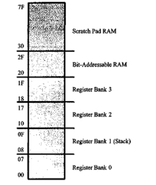
8051 consists of four register banks, such as Bank0, Bank1, Bank2, Bank3 which are selected by the PSW (Program Status Word) register. These register banks are present in the internal RAM memory of the 8051 microcontroller and are used to process the data when the microcontroller is programmed.
8051 by default is powered up with register bank 0; and, by using the Program Status Word (PSW), we can switch to other banks. The two bits of PSW are used for switching between the register banks. These two bits are accessed by the bit-addressable instructions SETB and CLR.
Based on the possible combinations of RS1 and RS0 of PSW, the register bank is changed accordingly, i.e., if RS1 and RS0 are 0, then the Bank 0 is selected. Similarly, Bank1, 2&3 are selected as per the values of RS1 and RS0.
Stack Memory Allocation
The stack is an area of random-access memory (RAM) allocated to hold temporarily all the parameters of the variables. The stack is also responsible for reminding the order in which a function is called so that it can be returned correctly. Whenever the function is called, the parameters and local variables associated with it are added to the stack (PUSH).
When the function returns, the parameters and the variables are removed (“POP”) from the stack. Therefore, a program’s stack size changes continuously while the program is running.
Stack:
The stack is a section of RAM used by the CPU to store information temporarily. This information could be data or an address. The CPU needs this storage area since there are only a limited number of registers.
The register used to access the stack is called the SP (stack pointer) register. The stack pointer is 8 bits wide, which takes values of 00 to FFH.
When the 8051 is powered up, the SP register contains value 07. This means that RAM location 08 is the first location used for the stack by the 8051. The storing of a CPU register in the stack is called a PUSH, and pulling the contents off the stack back into a CPU register is called a POP.
Pushing onto the stack
In the 8051 the stack pointer (SP) points to the last used location of the stack. When we push data onto the stack, the stack pointer (SP) is incremented by one.
The SP is decremented when data is pushed onto the stack.
For example, when PUSH is executed, the contents of the register are saved on the stack and SP is incremented by 1.
For example, the instruction “PUSH 1″ pushes register Rl onto the stack.
Show that the stack and stack pointer for the following. Assume the default stack area and register 0 is selected.
MOV R6, #25H
MOV R1,#12H
MOV R4, #0F3H
PUSH 6
PUSH 1
PUSH 4
Solution:
| After PUSH 6 | After PUSH 1 | After PUSH 4 |
0B | 0B | 0B | 0B |
0A | 0A | 0A | 0A F3 |
09 | 09 | 09 12 | 09 12 |
08 | 08 25 | 08 25 | 08 25 |
Start SP=07 SP=08 SP=09 SP=0A
Popping from the stack
Popping the contents of the stack back into a given register is the opposite process of pushing. With every pop, the top byte of the stack is copied to the register specified by the instruction and the stack pointer is decremented once.
Example:
Examine the stack shows the contents of the registers and SP after execution of the following instructions.
POP 3 ; POP stack into R3
POP 5; POP stack into R5
POP 2; POP stack into R2
Solution:
| After PUSH 6 | After PUSH 1 | After PUSH 4 |
0B 54 | 0B | 0B | 0B |
0A F9 | 0A F9 | 0A | 0A |
09 76 | 09 76 | 09 76 | 09 |
08 6C | 08 6C | 08 6C | 08 6C |
Start SP=0B SP=0A SP=09 SP=08
Internal Data Memory
In 8051 up to 256 bytes of internal data memory are available depending on the 8051 derivatives.
Locations available to the user occupy addressing space from 0 to 7Fh, i.e., first 128 registers and this part of RAM is divided in several blocks.
The first 128 bytes of internal data memory are both directly and indirectly addressable. The upper 128 bytes of data memory (from 0x80 to 0xFF) can be addressed only indirectly.
Since internal data memory is used for CALL stack also and there is only 256 bytes split over few different memory areas fine utilizing of this memory is crucial for fast and compact code.
Memory block in the range of 20h to 2Fh is bit-addressable, which means that each bit being there has its own address from 0 to 7Fh. Since there are 16 such registers, this block contains in total of 128 bits with separate addresses (Bit 0 of byte 20h has the bit address 0, and bit 7 of byte 2Fh has the bit address 7Fh).
Three memory type specifiers can be used to refer to the internal data memory: data, idata, bdata.
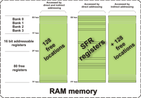
All 8051 microcontrollers have 4 I/O ports each comprising 8 bits which can be configured as inputs or outputs. Accordingly, in total of 32 input/output pins enabling the microcontroller to be connected to peripheral devices are available for use.
To configure a microcontroller pin as an input, it is necessary to apply a logic zero (0) to appropriate I/O port bit.
To configure a microcontroller pin as an input, it is necessary to apply a logic one (1) to appropriate port. In this case, voltage level on appropriate pin will be 5V (as is the case with any TTL input.
Port 0
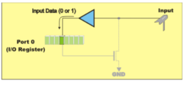
Figure . Input
If any pin of this port is configured as an input, then it acts as if it “floats”. Such an input has unlimited input resistance and indetermined potential.
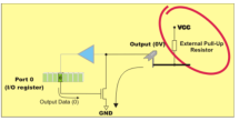
Figure . Output
When the pin is configured as an output, it acts as an “open drain”. By applying logic 0 to a port bit, the appropriate pin will be connected to ground (0V). To apply logic 1 (5V) on this output pin, it is necessary to build in an external pull-up resistor.
Port 1
P1 is a true I/O port, because it doesn't have any alternative functions as is the case with P0, but can be configured as general I/O only. It has a pull-up resistor built-in and is completely compatible with TTL circuits.
Port 2
P2 acts similarly to P0 when external memory is used. Pins of this port occupy addresses intended for external memory chip. This time it is about the higher address byte with addresses A8-A15. When no memory is added, this port can be used as a general input/output port showing features similar to P1.
Port 3
All port pins can be used as general I/O, but they also have an alternative function. To use these alternative functions, a logic one (1) must be applied to appropriate bit of the P3 register.
Register A/Accumulator
The Accumulator (sometimes referred to as Register A also) holds the result of most of arithmetic and logic operations. ACC is usually accessed by direct addressing and its physical address is E0H. Accumulator is both byte and bit addressable.

Register B
The major purpose of this register is in executing multiplication and division. The 8051 micro controller has a single instruction for multiplication (MUL) and division (DIV).
Ex: MUL A, B – When this instruction is executed, data inside A and data inside B is multiplied and answer is stored in A.
Note: For MUL and DIV instructions, it is necessary that the two operands must be in A and B.

Port Registers
4 Input/Output ports named P0, P1, P2 and P3 has got four corresponding port registers with same name P0, P1, P2 and P3. Data must be written into port registers first to send it out to any other external device through ports. Similarly, any data received through ports must be read from port registers for performing any operation. All 4 port registers are bit as well as byte addressable.
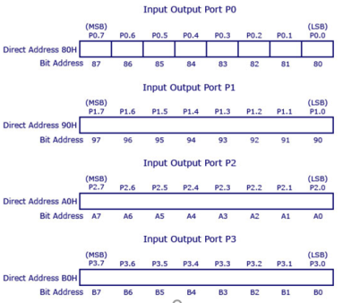
From the figure: -
- The physical address of port 0 is 80
- The physical address of port 1 is 90
- And that of port 2 is A0
- And that of port 3 is B0
Stack Pointer
Stack pointer is an 8-bit register, the direct address of SP is 81H and it is only byte addressable, which means you can’t access individual bits of stack pointer. The content of the stack pointer points to the last stored location of system stack. To store something new in system stack, the SP must be incremented by 1 first and then execute the “store” command. Usually after a system reset SP is initialized as 07H and data can be stored to stack from 08H onwards.
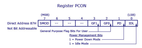
Setting bit 0 will move the micro controller to Idle mode and Setting bit 1 will move the micro controller to Power down mode.
Processor Status Word (PSW)
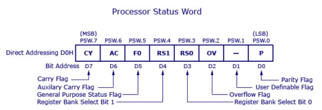
The picture below shows PSW register and the way register banks are selected using PSW register bits – RS1 and RS0. PSW register is both bit and byte addressable. The physical address of PSW starts from D0H. The individual bits are then accessed using D1, D2 … D7.
Bit No | Bit Symbol | Direct Address | Name | Function |
0 | P | D0 | Parity | This bit will be set if ACC has odd number of 1’s after an operation. If not, bit will remain cleared. |
1 | – | D1 |
| User definable bit |
2 | OV | D2 | Overflow | OV flag is set if there is a carry from bit 6 but not from bit 7 of an Arithmetic operation. It’s also set if there is a carry from bit 7 (but not from bit 6) of Acc |
3 | RS0 | D3 | Register Bank select bit 0 | LSB of the register bank select bit. Look for explanation below this table. |
4 | RS1 | D4 | Register Bank select bit 1 | MSB of the register bank select bits. |
5 | F0 | D5 | Flag 0 | User defined flag |
6 | AC | D6 | Auxiliary carry | This bit is set if data is coming out from bit 3 to bit 4 of Acc during an Arithmetic operation. |
7 | CY | D7 | Carry | Is set if data is coming out of bit 7 of Acc during an Arithmetic operation. |
There are 4 register banks named 0,1,2 and 3. Each bank has 8 registers named from R0 to R7. At a time only one register bank can be selected. Selection of register bank is made possible through PSW register bits PSW.3 and PSW.4, named as RS0 and RS1.These two bits are known as register bank select bits as they are used to select register banks.
SFR | Address | Function |
DPH | 83 | Data pointer registers (High). Only byte addressing possible. |
DPL | 82 | Data pointer register (Low). Only byte addressing possible. |
IP | B8 | Interrupt priority. Both bit addressing and byte addressing possible. |
IE | A8 | Interrupt enable. Both bit addressing and byte addressing possible. |
SBUF | 99 | Serial Input/Output buffer. Only byte addressing is possible. |
SCON | 98 | Serial communication control. Both bit addressing and byte addressing possible. |
TCON | 88 | Timer control. Both bit addressing and byte addressing possible. |
TH0 | 8C | Timer 0 counter (High). Only byte addressing is possible. |
TL0 | 8A | Timer 0 counter (Low). Only byte addressing is possible. |
TH1 | 8D | Timer 1 counter (High). Only byte addressing is possible. |
TL1 | 8B | Timer 1 counter (Low). Only byte addressing is possible. |
TMOD | 89 | Timer mode select. Only byte addressing is possible. |
Pins Of 8051
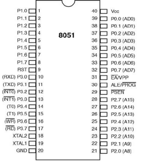
Figure. Pin Diagram of 8051
Pin out Description:
Pin 1-8 | PORT1- Each of these pins can be configured as an input or output. |
Pin 9 | RESET- A logic set on this pin disables the microcontroller and clears the contents of most registers. In other words, a positive voltage on this pin resets the microcontroller. |
Pin 10-17 | PORT -3: Similar to Port 1. Each pin serves as general output or input. Besides all of them have alternate functions. |
Pin 10 RXD | Serial Asynchronous Communication Input or Serial Synchronous Communication Output. |
Pin 11 TXD | Serial Asynchronous Communication Output or Serial Synchronous Communication clock output |
Pin 12 INT0 | External Interrupt 0 input |
Pin 14 INT1 | External Interrupt 1 input |
Pin 15 T0 | T0 Counter 0 clock input |
Pin16 T1 | T1 Counter 1 clock input |
Pin 17 RD | Read from external RAM |
Pin 18, 19 XTAL2, XTAL1 | Internal oscillator input and output. A quartz crystal which specifies operating frequency is usually connected to these pins. |
Pin 20 GND | Ground |
Pin 21-28 Port 2 | If there is no intention to use external memory then these port pins are configured as general inputs/outputs. In case external memory is used, the higher address byte, i.e., addresses A8-A15 will appear on this port. Even though memory with capacity of 64Kb is not used, which means that not all eight port bits are used for its addressing, the rest of them are not available as inputs/outputs. |
Pin 29 PSEN | If external ROM is used for storing program, then a logic zero (0) appears on it every time the microcontroller reads a byte from memory. |
Pin 30 ALE | Prior to reading from external memory, the microcontroller puts the lower address byte (A0-A7) on P0 and then activates the ALE output. After receiving signal from ALE pin, the external latch latches the state of P0 and uses it as a memory chip address. Immediately the ALE pin is returned to its previous logic state and P0 is now used as a Data Bus. |
Pin 31 EA | By applying logic zero to this pin, P2 and P3 are used for data and address transmission whether there is internal memory or not. It means that even if there is a program written to the microcontroller, it will not be executed. Instead, the program written to external ROM and executed. By applying logic one to the EA pin, the microcontroller will use both memories, first internal then external if present. |
Pin 32-39 PORT 0 | Similar to P2, if external memory is not used, these pins can be used as general inputs/outputs. Otherwise, P0 is configured as address output (A0-A7) when the ALE pin is driven high (1) or as data output (Data Bus) when the ALE pin is driven low (0). |
Pin 40 VCC | +5V power supply |
8051 microcontrollers have 4 I/O ports each of 8-bit, which can be configured as input or output. Hence, total 32 input/output pins allow the microcontroller to be connected with the peripheral devices.
- Pin configuration, i.e., the pin can be configured as 1 for input and 0 for output as per the logic state.
- Input/Output (I/O) pin − All the circuits within the microcontroller must be connected to one of its pins except P0 port because it does not have pull-up resistors built-in.
The CPU provides the address of the data desired, but it is the job of the decoding circuitry to locate the selected memory block. To explore the concept of decoding circuitry, we look at various methods used in decoding the addresses. We use SRAM or ROM for the sake of simplicity.
Memory chips have one or more pins called CS (chip select), which must be activated for the memory’s contents to be accessed. Sometimes the chip select is also referred to as chip enable (CE). In connecting a memory chip to the CPU, note the following points.
- The data bus of the CPU is connected directly to the data pins of the memory chip.
- Control signals RD (read) and WR (memory write) from the CPU are con
nected to the OE (output enable) and WE (write enable) pins of the memory chip, respectively. - In the case of the address buses, while the lower bits of the addresses from the CPU go directly to the memory chip address pins, the upper ones are used to activate the CS pin of the memory chip. It is the CS pin that along with RD/WR allows the flow of data in or out of the memory chip. No data can be written into or read from the memory chip unless CS is activated.
In SRAM and ROM, the CS input of a memory chip is normally active low and is activated by the output of the memory decoder. Normally memories are divided into blocks, and the output of the decoder selects a given memory block. There are three ways to generate a memory block selector: (a) using simple logic gates, (b) using the 74LS138, or (c) using programmable logics.
Each method is described below with some examples.
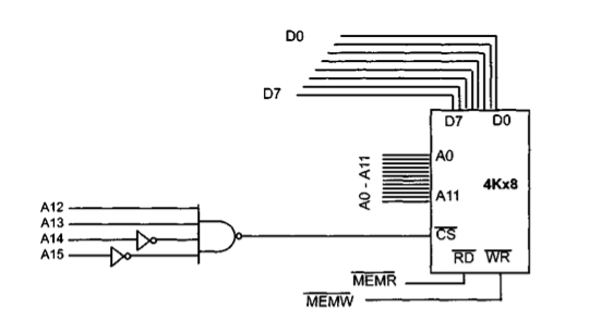
Figure - Logic Gate as Decoder
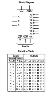
Figure - 74LS138 Decoder
Simple logic gate address decoder
The simplest method of constructing decoding circuitry is the use of a NAND gate. The output of a NAND gate is active low, and the CS pin is also active low, which makes them a perfect match. In cases where the CS input is active high, an AND gate must be used. Using a combination of NAND gates and inverters, one can decode any address range. An example of this is shown in Figure 14-4, which shows that A15 – A12 must be 0011 in order to select the chip. This results in the assignment of addresses 3000H to 3FFFH to this memory chip.
Using the 74LS138 3-8 decoder
This is one of the most widely used address decoders. The 3 inputs A, B, and C generate 8 active-low outputs YO – Y7. As shown in figure Each Y output is connected to CS of a memory chip, allowing control of 8 memory blocks by a single 74LS138.
In the 74LS138, where A, B, and C select which output is activated, there are three additional inputs, G2A, G2B, and Gl. G2A and G2B are both active low, and Gl is active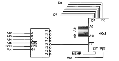
Figure. 74LS138 as Decoder
Using programmable logic as an address decoder
Other widely used decoders are programmable logic chips such as PAL and GAL chips. One disadvantage of these chips is that they require PAL/GAL software and a burner (programmer), whereas the 74LS138 needs neither of these. The advantage of these chips is that they can be programmed for any combination of address ranges, and so are much more versatile. This plus the fact that PALs and GALs have 10 or more inputs (in contrast to 6 in the 74138) means that they can accommodate more address inputs.
Circuit diagram to interface external data ROM with 8051
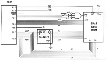
Code to interface external data ROM with 8051
ORG 0000H
MYXDATA EQU 1000H; 1000H, location where data is stored externally
COUNT EQU 100; To receive all 100 bytes of data
MOV DPTR, #MYXDATA; Move DPTR to 1000H location
MOV R0, #COUNT; Load R0 with 100
Rep: MOVX A, @DPTR; Copy data from location pointed by DPTR to acc
MOV P1, A; Move contents of acc to P1
INC DPTR; Inc DPTR to next ROM location
DJNZ R0, rep; Repeat until all 100 bytes are received
Stay: SJMP stay; Stay here forever
END
External RAM:
Step 1: Connect RD to OE of ext. RAM.
Step 2: Connect WR to WE of ext. RAM.
Step 3: Connect active low input of NAND gate to CE of external RAM, where the input to NAND gate is address lines A15, A14, and A13. We’ve given 0 1 0 to these lines to access the 8000H location of the external RAM.
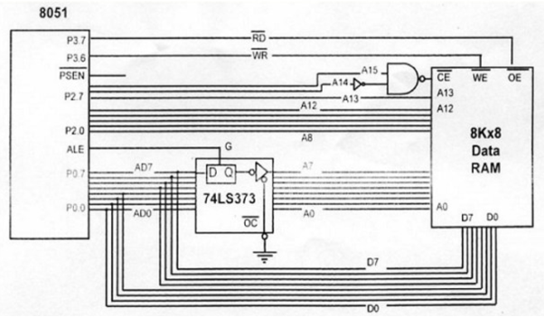
8051 addressing modes are classified as follows.
- Immediate addressing.
- Register addressing.
- Direct addressing.
- Indirect addressing.
- Relative addressing.
- Absolute addressing.
- Long addressing.
- Indexed addressing.
- Bit inherent addressing.
- Bit direct addressing.
Immediate addressing:
In this addressing mode the data is provided as a part of instruction itself.
That is the data immediately follows the instruction.
E.g., MOV A, #30H;
ADD A, #83;
Here # Symbol indicates that data is immediate.
Register addressing:
In this addressing mode the register will hold the data.
One of the eight general registers (R0 to R7) is used and specified as the operand.
E.g., MOV A, R0;
ADD A, R6
R0 – R7 will be selected from the current selection of register bank. The default register bank will be bank 0.
Direct addressing:
There are two ways to access the internal memory that is by using direct address and indirect address.
In direct addressing mode we not only address the internal memory but SFRs also.
In direct addressing, an 8-bit internal data memory address is specified as part of the instruction and hence, it can specify the address only in the range of 00H to FFH.
In this addressing mode, data is obtained directly from the memory.
E.g., MOV A,60h
ADD A,30h
Indirect addressing:
The indirect addressing mode uses a register to hold the actual address that is used in data movement.
Registers R0 and R1 and DPTR are the only registers that can be used as data pointers.
Indirect addressing cannot be used to refer to SFR registers.
Both R0 and R1 can hold 8-bit address and DPTR can hold 16-bit address.
E.g., MOV A, @R0
ADD A, @R1
MOVX A, @DPTR
Indexed addressing:
In indexed addressing, either the program counter (PC), or the data pointer (DTPR)—is used to hold the base address, and A is used to hold the offset address.
Adding the value of the base address to the value of the offset address forms the effective address.
Effective address = Base address + value of offset address.
Indexed addressing is used with JMP or MOVC instructions.
Look up tables are easily implemented with the help of index addressing.
E.g., MOVC A, @A+DPTR // copies the contents of memory location pointed by the sum of the accumulator A and the DPTR into accumulator A.
MOVC A, @A+PC // copies the contents of memory location pointed by the sum of the accumulator A and the program counter into accumulator A.
Relative Addressing:
Relative addressing is used only with conditional jump instructions. The relative address, (offset), is an 8-bit signed number, which is automatically added to the PC to make the address of the next instruction.
The 8-bit signed offset value gives an address range of +127 to —128 locations.
The jump destination is usually specified using a label and the assembler calculates the jump offset accordingly.
The advantage of relative addressing is that the program code is easy to relocate and the address is relative to position in the memory.
E.g., SJMP LOOP1 JC BACK
Absolute addressing:
Absolute addressing is used only by the AJMP (Absolute Jump) and ACALL (Absolute Call) instructions.
These are 2 bytes instructions.
The absolute addressing mode specifies the lowest 11 bit of the memory address as part of the instruction.
The upper 5 bit of the destination address are the upper 5 bit of the current program counter. Hence, absolute addressing allows branching only within the current 2 Kbyte page of the program memory.
E.g., AJMP LOOP1 ACALL LOOP2
Long Addressing:
The long addressing mode is used with the instructions LJMP and LCALL. These are 3-byte instructions. The address specifies a full 16-bit destination address so that a jump or a call can be made to a location within a 64 Kbyte code memory space.
E.g., LJMP FINISH LCALL DELAY
Bit Inherent Addressing:
In this addressing, the address of the flag which contains the operand, is implied in the opcode of the instruction.
E.g., CLR C; Clears the carry flag to 0
Bit Direct Addressing:
In this addressing mode the direct address of the bit is specified in the instruction. The RAM space 20H to 2FH and most of the special function registers are bit addressable. Bit address values are between 00H to 7FH.
E.g., CLR 07h; Clears the bit 7 of 20h RAM space
SETB 07H; Sets the bit 7 of 20H RAM space.
Key Takeaways
Addressing mode is a way to address an operand. Operand means the data we are operating upon.
References:
- Microprocessor Architecture, Programming, and ...Book by Ramesh S. Gaonkar
- 8085 Microprocessor: Programming and Interfacing Book by N. K. Srinath
- 8085 Microprocessors & Its Application Book by Nagoorkani