Unit - 1
Power Switching Devices
Diode
It is a simple semiconductor device that includes two layers, two terminals & a single PN junction, formed either in germanium or silicon crystal. The most common function of diode is to allow an electric current to pass in one direction while blocking in opposite direction.
In Power diodes, the junction can be formed among a heavily doped P+ layer & lightly doped N– layer whereas, the doping level in signal diode for both P-layer & N-layer is the same. Power diodes are used in numerous applications including rectifier, voltage clamper, voltage multiplier and etc. power diode has same symbol as that of simple diode.
Working
The working principle of power diode is similar to the normal PN junction diode. When the voltage of the anode terminal is high than the voltage of the cathode terminal, the diode conducts. The range of forwarding voltage drop in this diode is very small approximately 0.5V – 1.2V. In this mode, the diode works as a forward characteristic.
If the voltage of the cathode is high than the voltage of anode, the diode performs as blocking mode. In this mode, the diode performs like the reverse characteristic.
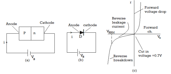
Fig: (a) P-N junction diode (b) symbol of diode (c) V-I characteristics of diode
V-I CHARACTERISTICS OF DIODE
When anode is positive with respect to cathode then diode is in forward bias mode. Initially diode current is zero with increase in applied voltage (Vs) from zero. When Vs is equal to threshold voltage Or cut in voltage, the forward anode current is very small. Beyond cut in voltage the diode current increases rapidly and diode is said to be in conduct.
When cathode is positive with respect to anode, diode is reverse biased. In this mode small reverse current called leakage current(mA) flows. As reverse voltage increases upto the breakdown voltage or Avalnche ,the leakage current also slowly increases. If leakage current or reverse current is not limited by series resistance then it may destroy the diode.to avoid the breakdown of diode, the diode should operate below specific peak respective reverse voltage (VRM) as shown in waveform above.
Thyristor
It is a four layer PNPN device, which has three PN junctions. Thyristor has three terminals: anode (positive terminal), cathode (negative terminal), and gate (control terminal). The gate controls the flow of current between the anode and cathode. It acts as bistable switch. Thyristors are used specifically for high power switching applications such as control of a.c. Power to the load, motor speed control, light dimmers, etc.
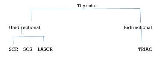
There are two main types of thyristors a) Unidirectional which conducts in forward direction only. Examples are Silicon Controlled Rectifiers (SCR’s), Light Activated Silicon Controlled Rectifiers (LASCR’s) and Silicon control Switch (SCS). b) Bidirectional which can conducts in both forward as well as in reverse direction. Example is Triode A.C Switch (TRIAC).
Working of Thyristor
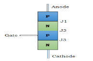
A Thyristor acts like a diode. It has two layers of semiconductors namely p-type and n-type sandwiched together to form a junction. The anode is connected to the outer p-layer, cathode to the outer n-layer and gate to the internal p-layer. It has 3 junctions namely J1, J2, J3 as shown below.

(a) (b)
Fig (a) layered structure of thyristor (b) symbol of thyristor
When the anode is at positive potential with respect to cathode, no voltage is applied to the gate. The junctions J1, J3 is forward biased and J2 is reverse biased. So no conduction takes place here.
Now, when the positive potential is increased beyond the breakdown voltage, breakdown of junction J2 takes place and it starts conducting. Once the breakdown has occurred, it continues to conduct irrespective of the gate voltage, until the potential at the anode is removed or current through the device is made less than the holding current.
Now when a positive potential is applied at the gate terminal with respect to cathode, the breakdown of junction J2 takes place. To switch on the Thyristor quickly, an appropriate potential value has to be selected. The gate acts as a controlling electrode. When a small voltage known as gate pulse is applied to its gate, the device is triggered into conduction state .This continues until the voltage across the device is reversed or removed.
The gate trigger current varies inversely with the gate voltage and a minimum gate charge is required to trigger it. Thus the switching of thyristor can be controlled through its gate pulse.
Two Transistor Analogy of Thyristor
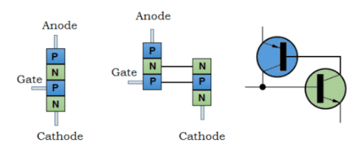
The thyristor is designed by cascading two transistor as shown below. The collector current from the NPN transistor is fed directly to the base of PNP transistor, while the collector current of PNP transistor is fed to the base of NPN. These interconnected transistors rely on each other for conduction.
So for one of the transistors to conduct, a base current is required. When the thyristor’s anode terminal is negative with respect to cathode, the NP junction becomes forward biased and the PN junction becomes reverse biased.
(a) (b) (c)
Fig: (a) basic structure (b)two transistor model (c) two transistor circuit
Here, the flow of reverse current is blocked until a breakdown voltage is applied. After breakdown voltage, it starts to conduct without the application of gate signal. This is one of the negative characteristics of thyristor as it triggers into conduction by a reverse break over voltage.
When the anode terminal is made positive with respect to cathode, the outer junctions are forward biased and the centre NP junction is reverse biased and blocks the forward current. So to trigger it into conduction, a positive current is applied to the base of transistors.
The two transistors are connected in a regenerative loop and this force the transistor to conduct to saturation. Thus, it can be said that a thyristor block current in both the direction of an AC supply in it’s OFF state and can be turned ON by the application of positive current to the base of transistor.
V-I Characteristics of Thyristor
The V_I characteristics of thyristor is shown in fig below. Thyristor can either be forward biased state or reverse biased state.
Forward Biased State
When anode is made positive, the PN junctions at the ends are forward biased and centre junction (NP) becomes reverse biased. It will stay in blocked (OFF) mode (also known as Forward Blocking Stage) till the time it is triggered by Gate current pulse or the applied voltage reaches the forward breakover voltage. The thyristor can trigger ON by following two methods.
1. Triggering by Gate Current Pulse – When it is triggered by the gate current pulse, it starts conducting and will act as a close switch. The thyristor remains in the ON-state, i.e. it remains in the latched state. Here the gate loses its control to turn off the device.
2. Triggering by Forward Breakover Voltage – When a forward voltage is applied, a leakage current starts to flow through the blocking (J2) in the middle junction of thyristor. When voltage exceeds the forward break over voltage or critical limit, then J2 breaks down and it reaches to the ON state.
When the Gate current (Ig) is increased, it reduces the blocking area and so the forward break over voltage is reduced. It will turn ON when a minimum current called latching current is maintained.When the gate current Ig=0 and anode current falls below a certain value called holding current during the ON state, it again reaches to its forward blocking state.
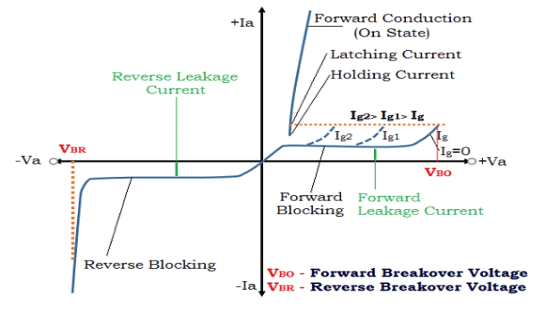
Fig: V-I characteristics of Thyristor
Reverse Biasing state
If the anode is negative with respect to cathode, i.e., with the application of reverse voltage, both PN junctions at the end i.e. J1 and J3 become reverse biased and the centre junction J2 becomes forward biased. Only a small leakage current flows through it. This is the reverse voltage blocking mode or OFF state of Thyristor.
When the reverse voltage is increased further, then at a certain voltage, avalanche breakdown of J1 and J2 occurs and it starts conducting in the reverse direction. The maximum reverse voltage at which a thyristor starts conducting is known as Reverse Breakdown Voltage.
MOSFET (Metal Oxide Silicon Field Effect Transistor or Metal Oxide Semiconductor Field Effect Transistor)
MOSFET has three terminals source(S), drain (D), and gate (G). The gate (G) terminal of MOSFET is insulated from channel. The circuit symbol and construction is shown below. Here arrow indicated the flow of electrons. MOSFET is voltage controlled device and as its operation depends on majority carriers only it is unipolar device. MOSFET has large gate circuit impedance which protects secondary breakdown.
Power MOSFET has two types n-channel enhancement type MOSFET and p-channel enhancement type MOSFET. As n-channel enhancement type MOSFET has higher mobility of electrons it is more preferred in applications.
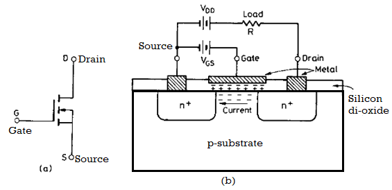
Fig (a) symbol of n-channel EMOSFET (b) basic structure of n-channel EMOSFET
Working of n-channel enhancement type MOSFET
The n-channel Enhancement MOSFET is similar to that of p-channel Enhancement MOSFET but only operationally and constructional these two are different from each other. In N Channel Enhancement MOSFET a lightly doped p-type substrate forms the body and source and drain regions are heavily doped with n-type impurities. Here body and source commonly to the ground potential. Now, a positive voltage is applied to the gate terminal. Due to positive gate and corresponding capacitive effect, free electrons i.e. minority carriers of the p-type substrate get attracted towards the gate and form a layer of negative uncovered ions there just below the dielectric layer by recombining these free electrons with holes. If we continually increase the positive gate voltage, after the threshold voltage level, the recombination process gets saturated and then free electrons start to accumulate at the place to form a conductive channel of free electrons. The free electrons also come from the heavily doped source and drain n-type region.
Now if we apply a positive voltage at the drain, current start flowing through the channel. The resistance of the channel depends on the number of free electrons in the channel and the number of free electrons in the channel again depends on the gate potential of the device. As the concentration of free electrons forms the channel, and the current through the channel gets enhanced due to increase in gate voltage, it is named as N – Channel Enhancement MOSFET.
MOSFET Characteristics
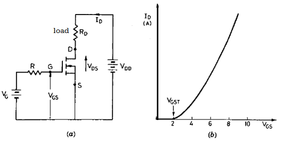
Fig: (a) n-channel enhancement type power MOSFET (b) transfer characteristics
a) Transfer Characteristics
This characteristics shows variation between drain current ID with respect to voltage across gate to source terminal VGS . From the fig it is clear that below threshold voltage VGST the MOSFET is OFF.
b) Output Characteristics
This Characteristics shows variation of drain current ID as a function of applied drain to source voltage VDS keeping VGS constant for low values of VDS, the graph of ID-VDS is almost linear, indicates constant value of on resistance RDS=VDS/ID. For given value of VGS, if VDS increases the drain current is nearly constant showing flat response.
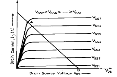
Fig: output characteristics
IGBT (Insulated Gate Bipolar Transistor)
IGBT is a fusion between BJT and MOSFET, having the input characteristics of a BJT and output characteristics of a MOSFET. It is a three-terminal semiconductor switching device that can be used for fast switching with high efficiency in many types of electronic devices. These devices are mostly used in amplifiers for switching/processing complex wave patters with pulse width modulation (PWM).
The IGBT is divided into two types based on the n+ buffer layer, the IGBTs that are having the n+ buffer layer is called the Punch through IGBT (PT-IGBT), the IGBTs that does not have an n+ buffer layer are called the Non-Punch Through- IGBT (NPT- IGBT).
Operation of IGBT as a Circuit
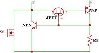
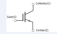
Since IGBT is a combination of BJT and MOSFET lets look into their operations as a circuit diagram here. The below diagram shows the internal circuit of IGBT which includes two BJT and one MOSFET and a JFET. The Gate, Collector, and Emitter pins of the IGBT are marked below.
(a) (b)
Fig (a) IGBT symbol (b) basic Structure of IGBT
The collector of the PNP transistor is connected to the NPN transistor through a JFET, the JFET connects the collector of the PNP transistor and the base of the PNP transistor. These transistors are arranged in a way to form a parasitic thyristor set up to create a negative feedback loop. The Resistor RB is placed to short the base and emitter terminals of the NPN transistor to ensure that the thyristor doesn’t latch-up which leads to the latch-up of the IGBT. The JFET used here will signify the structure of current between any two IGBT cells and allows the MOSFET and supports most of the voltage.
Characteristics of IGBT
The IGBT is a Voltage controlled and it is unidirectional device.
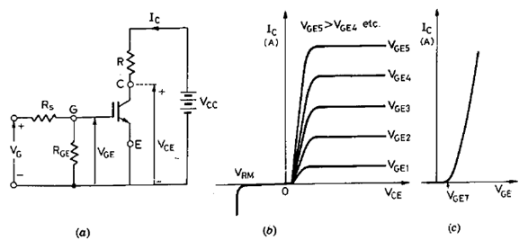
Fig (a) IGBT circuit diagram (b) static V-I characteristics (c) transfer characteristics
The static V-I char. Is plot of collector current IC versus voltage across collector and emitter terminal VCE keeping voltage of gate emitter VGE terminal constant. In forward direction the output char. Is same as of BJT char. But here controlling parameter is VGE as IGBT is voltage controlled device.
The transfer char. Is plot of collector current IC versus voltage across gate and emitter terminal VGE. This char. Is same as that of power MOSFET. Below threshold voltage VGET , the IGBT is OFF state. When IGBT is in OFF state, junction J2 blocks forward voltage and in case of reverse voltage appear across emitter J1 blocks it.
Triggering means turning ON of a device from its off state. Turning ON of a thyristor refers to thyristor triggering. Thyristor is turned on by increasing the anode current flowing through it. The anode current can be increase by following ways.
Forward breakover Voltage Triggering: - In this, the applied forward voltage is gradually increased beyond a point known as forward break over voltage VBO and gate is kept open.
Gate Triggering: - This method of thyristor triggering is widely used method because of ease of control over the thyristor gate triggering of thyristor allows to turn of the thyristor whenever we wish. Here a gate signal is applied to the thyristor. The thyristor will turn on when gate signal is applied to it and it will be in forward biased. Once the thyristor starts conducting, the gate loses its control over the device and the thyristor continues to conduct. This is because of regenerative action that takes place within the thyristor when gate signal is applied.
When the thyristor is forward biased, and a gate signal is injected by applying positive gate voltage is applied between gate and cathode terminals, then the thyristor is turn on.
Dv/dt Triggering:- In this type of triggering, if the rate of rise of anode to cathode voltage is high, the charging current through the capacitive junction is high enough to turn on the thyristor. A high value of charging current may destroy the thyristor hence the device must be protected against high dv/dt.
Light Thyristor Triggering: - In this type of triggering, the rays of light are allowed to strike the junctions of the thyristor. This results in an increase in the number of electron-hole pair and thyristor may be turned on. The light-activated SCRs (LASER) are triggered by using this method.
Thermal Thyristor Triggering: - If the temperature of the thyristor is high, it results in increase in the electron-hole pairs. Which in turn increase the leakage current α1 and α2 to raise. The regenerative action tends to increase (α1 + α2) to units and the thyristor may be turned on. This type turn on is not preferred as it may result in thermal turn away and hence it is avoided.
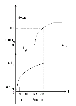
Fig. Shows the waveform of anode current after the application of gate signal. t-on is the turn on delay time. The turn on delay time is the time interval between the application of gate signal and conduction of thyristor. The turn on delay time ton is defined as the time interval between 10% of steady state gate current 0.1Ig and 90% of steady state thyristor on state current 0.9IT ton is the sum of delay time td and rise time tr. The delay time td is defined as the time interval between 10% of steady state gate current (0.1 Ig) and 10% of on state thyristor current (0.1IT). The rise time tr is defined as the time taken by the thyristor anode current from 10% of thyristor on state current (0.1IT) to 90% of on state thyristor current (0.9IT).
While designing gate thyristor triggering circuit following points should be kept in mind.
- When thyristor is turned on the gate signal should be removed immediately. A continuous application of gate signal even after the triggering on and thyristor would increase the power loss in the gate junction.
- No gate signal should be applied when thyristor is reversed biased.
- The pulse width of the gate signal should be longer than the time required for the anode current to rise to the holding current value IH.
Commutation means the process of turning off a thyristor. In all the commutation techniques, the anode current is maintained below the holding current for a sufficiently long time, so that all the excess carriers in the four layers are swept out or recombined.
There are mainly two types of SCR commutation techniques: Natural Commutation and Forced Commutation.
Natural Commutation of SCR:
Natural Commutation of SCR is the process of turning off an SCR without using additional commutation circuitry. This commutation technique only occurs in AC circuit. For better understanding, let us consider an SCR circuit energized from AC source.
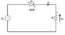
When SCR is conducting, the current will pass through zero after every positive half cycle. After that, the AC source then applies a reverse voltage across the terminals of SCR till the beginning of second cycle. If the time of application of reverse voltage applied by the AC source is more than the SCR turn-off time, then SCR will get turned off.
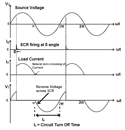
From the above waveform, following points can be noted:
- SCR is fired or gated at an angle of δ on the Source Voltage.
- The waveform of output current or SCR anode current (Io = Vo / R) is sinusoidal as the load is resistive load.
- When the AC Source Voltage reaches zero at ωt = π, the load current or SCR anode current becomes zero.
- After ωt = π, the source voltage becomes negative and hence, the voltage across SCR also becomes negative. Thus SCR is reversed biases from ωt = π to ωt = 2π i.e. for a time period of tc = (π / ω). This time tc is called Circuit Turn Off time.
- If tc is more than the SCR turn off time, then SCR will get turned off.
Thus we see that, the SCR is getting turned off due to the natural tendency of AC. This is the reason, this type of commutation technique is called Natural Commutation. It should also be noted that, no additional circuitry is required in this commutation technique. This commutation technique is basically the Class-F commutation (you might encounter in many literature) technique which is also known as Line Commutation of SCR.
Forced Commutation of SCR:
Unlike natural commutation, an external circuitry is required to forcibly bring the SCR anode current below holding current and keeping SCR reversed biased for a period more than the SCR / thyristor turn off time. This technique is applied for DC circuit. The commutation circuitry for forced commutation comprises of Inductor and capacitor. Forced commutation is applied to Choppers and Inverters. There are several forced commutation techniques.
- Class-A Commutation (also known as Load Commutation)
- Class-B Commutation (also known as Resonant Pulse Commutation)
- Class-C Commutation (often called Complimentary Commutation)
- Class-D Commutation or Impulse Commutation
- Class-E Commutation or External Pulse Commutation
A gate driver is a power amplifier that accepts a low-power input from a controller IC and produces a high-current drive input for the gate of a high-power transistor such as an IGBT or power MOSFET.
Need of gate driver
The structure of an IGBT/power MOSFET is such that the gate forms a nonlinear capacitor. Charging the gate capacitor turns the power device on and allows current flow between its drain and source terminals, while discharging it turns the device off and a large voltage may then be blocked across the drain and source terminals. The minimum voltage when the gate capacitor is charged and the device can just about conduct is the threshold voltage (VTH). For operating an IGBT/power MOSFET as a switch, a voltage sufficiently larger than VTH should be applied between the gate and source/emitter terminals.
Power MOSFETs and IGBTs are simply voltage driven switches, because their insulated gate behaves like a capacitor.
Driving a Gate
As shown below, driving a gate consists of applying different voltages: 15V to turn on the device through S1, and 0V to turn off the device through S2.
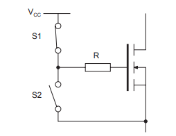
The voltage at which the gate voltage remains during switching is known as the Miller voltage, Vgm. In most applications, this voltage is around 4 to 6V, depending on the level of current being switched. This feature can be used to control the switching waveforms from the gate drive.
MOSFET and IGBT turn-ON / turn-OFF
When turned on under the same conditions, IGBTs and MOSFETs behave in exactly the same way, and have very similar current rise and voltage fall times.
However, at turn-off, the waveforms of the switched current are different, as shown in figure below. At the end of the switching event, the IGBT has a “tail current” which does not exist for the MOSFET. This tail is caused by minority carriers trapped in the “base” of the bipolar output section of the IGBT causing the device to remain turned on.
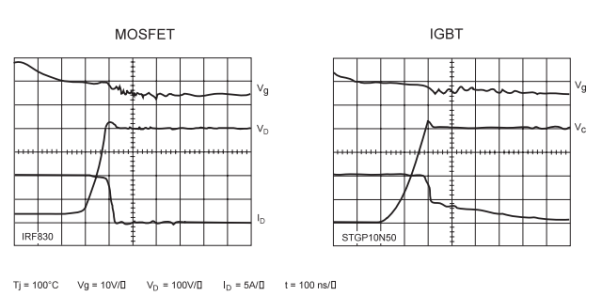
Fig: MOSFET and IGBT turn-OFF waveform
Unlike a bipolar transistor, it is not possible to extract these carriers to speed up switching, as there is no external connection to the base section, and so the device remains turned on until the carriers recombine naturally. Hence the gate drive circuit has no effect on the tail current level and profile.
References:
- M. H. Rashid, “Power electronics: circuits, devices, and applications”, Pearson Education India, 2009.
- N. Mohan and T. M. Undeland, “Power Electronics: Converters, Applications and Design”, John Wiley & Sons, 2007.
- R. W. Erickson and D. Maksimovic, “Fundamentals of Power Electronics”, Springer Science& Business Media, 2007.
- L. Umanand, “Power Electronics: Essentials and Applications”, Wiley India, 2009.