Unit - 2
Thyristor Rectifiers
A rectifier is a circuit that converts an AC signal into a unidirectional signal. A rectifier is a type of ac–dc converter. A rectifier may also be considered as an absolute value converter. If Vs is an ac input voltage, the waveform of the output voltage Vo would have the same shape, but the negative part will appear as a positive value. That is, Vo = |Vs|. Depending on the type of input supply, the rectifiers are classified into two types: (1) single phase and (2) three phase. A single-phase rectifier can be either a half wave or a full wave.
Single-phase half-wave rectifier
Single Phase Half Wave Controlled Rectifier, as the name suggests, is a rectifier circuit which converts AC input into DC output only for positive half cycle of the AC input supply. The word “controlled” means that, we can change the starting point of load current by controlling the firing angle of SCR. Firing of SCR simply means, the SCR turn ON at certain point of time when it is forward biased.
A simple circuit diagram of Single Phase Half Wave Controlled Rectifier is shown in figure below.
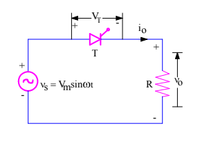
v0 = Load output voltage
i0 = Load current
VT = Voltage across the thyristor T
Following points must be consider for designing controlled rectifier:
a) The important condition is, an SCR will only get turned ON when it is forward biased and fired or gated.
b)SCR will only turn off when current through it reaches below holding current and reverse voltage is applied for a time period more than the SCR turn off time.
Let us assume that thyristor T is fired at a firing angle of α. When wt = α, gate signal will be applied and SCR will start conducting. Refer the following figure.
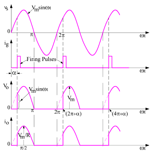
Thyristor T is forward biased for the positive half cycle of supply voltage. The load output voltage is zero till SCR is fired. Once SCR is fired at an angle of α, SCR starts conducting. But as soon as the supply voltage becomes zero at ωt = π, the load current will become zero and after ωt = π, SCR is reversed biased. Thus thyristor T will turn off at ωt = π and will remain in OFF condition till it is fired again at ωt = (2π+α).
A firing angle is defined as,” the angle measured from the instant that gives the largest average output voltage to the instant it is triggered”. As shown in fig, the SCR is fired at ωt =0, 2π, 4 π,etc, the average load (output) voltage is highest so the firing angle should be measured at this instants.
A single phase half wave circuit is one which produces only one pulse of load current during one cycle of source voltage.
Average voltage V0 across load R for single phase half wave circuit in terms of firing angle α is given by

The maximum value of V0 occurs at α=00,

Average load current

For some different types of loads such as electric heater and incandescent lamp, the rms value of load voltage and load current is given as


The value of rms current  is
is

Power delivered to resistive load = (rms load voltage)* ( rms load current)

Input volt-amperes = (rms source voltage)* (total rms line current)

Input power factor 

Single phase full wave rectifier
The disadvantages of single phase half wave rectifier or single phase one pulse converter is minimised by single phase full wave or single phase two pulse converters. There are two basic configurations for full wave controlled converters, a) Mid- point converter (uses an input transformer with two windings for each input phase windings) b) A three phase 6 pulse mid- point converters as shown below.

Fig (a) single phase two pulse full wave converter (b) three phase 6 pulse mid -point converter
In single phase two pulse converters, voltage at the output terminals can be controlled by adjusting the firing angle delay of SCR. The circuit diagram for single phase full wave converter using center-tapped transformer is shown below. When terminal a is positive w.r.t n, terminal n is positive w.r.t terminal b. Therefore Van=-Vbn as n is mid- point of secondary winding. Here we assume that turns ratio of primary to secondary winding is unity.
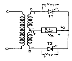
Fig: single phase full wave converter
Here SCR T1 and T2 are forward biased during positive and negative half cycles of supply. Suppose T2 is already conducting, after ωt =0, Van is positive, therefore T1 is forward biased, and when fires at α, T1 gets turned ON. At this firing angle α, supply voltage vs =2Vm Sin α , reverse biases T2 which turns OFF T2. Here T1 is called incoming thyristor (SCR) and T2 is outgoing thyristor. When T1 is forward biased, T2 is reversed biased, so load current is also transferred from T2 to T1. This process of turned OFF of SCR (T2) by natural reversible ac supply voltage is called natural commutation or Line commutation.
It is seen from the output voltage waveform V0, the average value of output voltage is given by

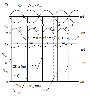
Fig: voltage and current waveforms of single phase full wave converter
The following observation can be made from diagram
(a) For commutation of SCR (T2)) need to be done, the incoming SCR (T1) must be forward biased and T2 should be reversed biased.
(b) When incoming SCR (T1) is turned ON, current is transferred from outgoing SCR (T2) to Incoming SCR (T1).
(c) The circuit turn-OFF time must be greater than SCR turn-OFF time.
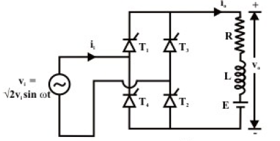
Fig (a) circuit diagram of single phase bridge converter
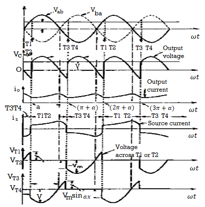
Fig (b) voltage and current waveform for continuous load current
Fig (a) shows the circuit diagram of a single phase fully controlled bridge converter. The single phase fully controlled bridge converter is designed by replacing all the diode of the corresponding uncontrolled converter by thyristors. Thyristors T1 and T2 are fired together while T3 and T4 are fired 180º after T1 and T2. From the circuit diagram, it is clear that for any load current to flow at least one thyristor from the top group (T1, T3) and one thyristor from the bottom group (T2, T4) must conduct. It can also be noted that neither T1T3 nor T2T4 can conduct simultaneously. For example whenever T3 and T4 are in the forward blocking state and a gate pulse is applied to them, they turn ON and at the same time a negative voltage is applied across T1 and T2 commutating them immediately. Similar for T1 and T2. For the same reason T1T4 or T2T3 cannot conduct simultaneously. Therefore, the only possible conduction modes when the current i0 can flow are T1T2 and T3T4. It is possible that at a given point no one of the thyristors conduct. This situation will typically occur when the load current becomes zero in between the firings of T1T2 and T3T4. Once the load current becomes zero all thyristors remain off. In this mode the load current remains zero. Consequently the converter is said to be operating in the discontinuous conduction mode. It is to be noted that whenever T1 and T2 conducts, the voltage across T3 and T4 becomes –Vi. Therefore T3 and T4 can be fired only when Vi is negative i.e, over the negative half cycle of the input supply voltage. Similarly T1 and T2 can be fired only over the positive half cycle of the input supply. The voltage across the devices when none of the thyristors conduct depends on the off state impedance of each device. Under normal operating condition of the converter the load current may or may not remain zero over some interval of the input voltage cycle. If i0 is always greater than zero then the converter is said to be operating in the continuous conduction mode. In this mode of operation of the converter T1T2 and T3T4 conducts for alternate half cycle of the input supply. However, in the discontinuous conduction mode none of the thyristors conduct over some portion of the input cycle. The load current remains zero during that period.
The Average value output voltage V0 is given by

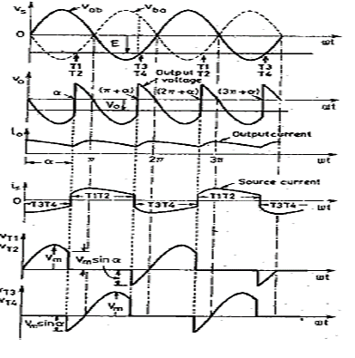
Fig (c): voltage and current waveform for single phase converter for α> 900
The fig (c) shows that if α> 900, V0 is negative. If the load circuit emf E is reversed, this source E will feed power back to ac supply. This operation of full converter is known as inverter operation. The firing angle delay greater than 900 is called line-commutated inverter.
During 0 to α, ac source voltage vs is positive but ac source current is negative, therefore power flows from dc to ac source. From α to π, both vs and is are positive, therefore power flows from ac to dc source. But net power flows is from dc source to ac source, because (π - α) < α, as shown in fig (c).
Advantages of bridge converter over mid-point converter
(a) SCR are subjected to a peak inverse voltage of 2Vm in mid-point converter and Vm in full wave converter. Thus power handled by mid-point converter is about half of that of bridge converter.
(b) In mid-point converter, each secondary should be able to supply the load power. This is not the case with single phase bridge converter.
Ex. A single phase full converter bridge is connected to RLE load. The source voltage is 230V, 50 Hz. The average load current of 10A is continuous over the working range. For R=0.4Ω and L=2mH, Compute
(a) firing angle delay for E=120V
(b) firing angle delay for E= -120V
Ans:
(a) For E=120V, the full wave converter is operating as a controlled converter.


For  , power flows from ac sources to be load
(b) For E =-120V the full converter is operating as a line commutated inverter

For  the power flows from dc sources to ac load
For large power loads, 3-phase converters are commonly used. There are three types of 3-phase converters. 1) 3-phase half wave converter, 2) 3-phase semi -converter, 3) 3-phase full converter and 3-phase dual converter. 3-phase half wave converter is rarely used in industrial application as it produces dc components in the supply current. Semi-converter and full wave converters are commonly used converter industrial applications. A dual converter is only used when reversible dc drives with power ratings of several MW are required.
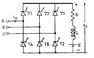
Fig(a): power circuit for 3-phase bridge converter
The 3-phase input supply is connected to terminals A, B, C and the load RLE is connected across the output terminals. This circuit works as 3-phase converter for firing angle delay 00<α ≤ 900 . A 3-phase is preferred where regeneration of power is required. The numbering of SCR’s shown in fig is 1, 3, 5 for positive group and 2, 4, 6 for negative group.
For α= 00 , T1, T2,..T6 behaves like a diodes. This is shown in waveform below in fig(b). Note that for α= 00, T1 is triggered at wt= π/6, T2 at 900, T3 at 1500, and so on. The load voltage waveform is shown in (c).
For α= 600, the conduction sequence of SCR’s T1 to T6 is shown in below fig(d). Here T1 is triggered at wt=300+600=900, T2 at 900+600=1500 and so on. Note that each SCR conducts for 1200 , when T1 is triggered, T5 is turned OFF and T1is turned ON. T6 is already conducting. As T1 is connected to terminal A and T6 is connected to B, the voltage vab appears across load and it varies from 1.5Vm to zero. H ere Vmp is a maximum phase voltage.
When T2 is turned ON, T6 is commutated from negative group and T1 is already conducting. As T1 and T2 are connected to terminal A and C, the voltage vac appears across load. The same sequence is continued for other SCRs.
As both group of SCR’s are fired at an interval of 600, this means that commutation occurs every 600, alternatively in upper and lower group of SCR’s. At any time, two SCR’s, one from positive group and other from negative group, must conduct together for source to energise that load. For ABC phase sequence of 3-phase supply, SCR’s conducts in pairs; T1and T2, T2 and T3 and so on.
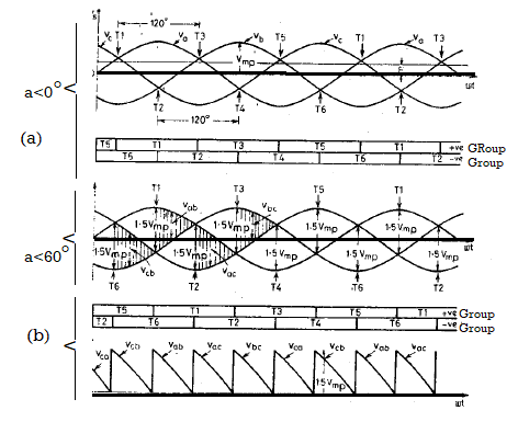
Fig(c): voltage waveform and conduction of SCR’s in 3-phase converter.
The following fig(d) shows line voltage vab, vac, vbc, vba, etc which makes for clear idea of conduction of SCR’s.
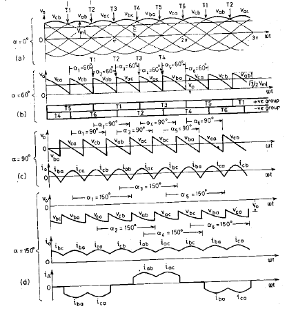
Fig(d): voltage and current waveform of 3-phase bridge converter for different firing angles
For α= 600 ,T1 is ON at wt=60+60=1200, T2 at wt=1800, T3 at wt=2400 and so on. When T1 is turned ON, T5 is turned OFF and T6 is already conducting. As T1 ane connected to A and B, load voltage is vab. When T2 is turned ON, T6 is commutated. In this manner load voltage waveform can be drawn with the turning ON or OFF of other SCR’s in sequence.
For α= 900, the load voltage is symmetrical bout the reference line wt, therefore its average value is zero.
For α=1500, T1 is triggered at wt=2100, T2 at wt=2700 and so on. It is observed from fig that the output voltage is reverse in polarity. This means that dc source is delivering power to ac source. This is called line commutated inverter operation of 3-phase full bridge converter.
Expression for Average output voltage V0
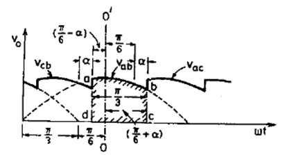
Fig: Output voltage waveform for 3-phase full converter
The average output voltage V0 can be obtained from above output voltage waveform. Note that periodicity of output voltage is π/3 radians. Average value of output voltage is obtained by finding the dashed area abcd over a periodic cycle and then dividing it by the periodic time.
With OO’ as the origin at the maximum value of vab, V0 is given by,


Here, Vm is maximum line voltage.
If sine function is used for the source voltage, then vab= Vm sin wt because vab= 0 at wt=0.


It is observed from fig(b) that source current for phase A i.e. iA(or for any other phase) flows for 1200 for every 1800.therefore in case of output current is assumed at I0, the rms value of source current is

Example :- (a) a 3- phase full converted charger a battery from a three phase supply of 230 V, 50 HZ . The battery emf is 200 V and its internal resistance is 0.5 . On account of inductance connected in series with the battery , charging current is constant at 20 A . Compute the firing angle delay and the supply power factor
b. In case it is desired that power flows from dc sources to ac load in part ( a) , find the firing angle delay for the same current
Solution;- (a) the battery terminal voltage  is
is


For constant load current  =20A , fig 6.26 (d) reveals that supply current is of rectangular (or square) wave of amplitude 20 A. It is also seen from this figure that flows for 120 ( or 2
 radians) over every half cycle of
  radians.
Rms value of the supply current over  radians is

Rms value of output current ,  =20A
=20A
Power delivered to load


Now 
(c) When battery is delivering power , then

When power flows from dc sources to ac load , the 3- phase full converter then works as a 3- phase line communted inverter


Example:- (a) A 3- phase full converted feed powers to a resistive load of 10 . For a firing angle delay of 30 , the load takes 5 kW . Find the magnitude of per phase input supply voltage
(b) Repeat part (a) in case a large reactor in series with load renders the load current ripple free
Solution :- (a) for a resistive load, output current waveform is of the same shape as that of the output voltage wave. Is is seem from fig. 6.26 that for a > 60 the output voltage and output current would be discontinuous for resistive load . However for a <60
 output voltage and current are continuous . From fig 6.27 , the rms value of output voltage
  is given by


For this example ,  =500 warts and
  =
= 


Per phase voltage

(b). For a constant load current , average load current  =rms load current


Three phase converters using diode or Silicon Controlled Rectifier (SCR) are widely employed to convert the commercial AC supply to DC. Such converters inject harmonics into the power supply system and thereby distort supply system voltage waveform. A simple input current wave-shape improvement technique using a shunt connected harmonic current compensator is presented in this work, intended to reduce the Total Harmonic Distortion (THD) of input current of three phase diode and SCR phase controlled rectifiers operating with inductive loads, by matching them to the specific converter as a combined package. The compensator proposed here comprises of a three-limb voltage source converter using Insulated Gate Bipolar Transistor (IGBT), working on instantaneous current and voltage measurements of the compensator only and not of the load. The technique uses a simple feed-forward control for AC source current harmonic compensation of rectifiers without monitoring the AC line currents, i.e., use of on-line computation. The proposed system is simulated and tested on a laboratory prototype. The measured input current THD values without additional line filters are found to be below 8.3%, which is within acceptable limits, proving that the new technique is capable of compensating pre-determined current harmonics of diode or SCR rectifiers.
We need to reduce the input line current harmonics in order to follow with the standard. If the power factor of an electric load is lower than unity, the apparent power which is delivered to the load which is connected to power system is greater than the real power drawn by the load. The real power is only doing the useful work for the load to run, and but the apparent power which gives the current that is flowing into the load which is connected to the power system, for a given load voltage. PFC is a technique which is used to make the power factor to be increased to a value which is near to the unity by using few elements in the PFC methods.
POWER FACTOR:
Input power factor of electrical power system is defined as

For purely sinusoidal voltage and current,

Let us consider for an input voltage of V and a line current of I, VI cos Ø , VI sin Ø and VI is the active power in kW, reactive power in kVAR and apparent power in KVA.
Power factor is the measure of how much the input line current and input voltages are distorted from the original shape and phase shift between them. Consider an inductor circuit, which draws a current I from the supply mains lagging behind the supply voltage V by an angle
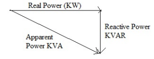
Fig: power triangle

When the load is having the nonlinear characteristics then definitely the line current follows the non-sinusoidal nature. For the sinusoidal voltage & non-sinusoidal current, the PF can be expressed as follows


Kp describes the harmonic content of the current with respect to the fundamental. Therefore, the PF depends on both harmonic content and displacement factor. Kp Is referred to as purity factor or distortion factor
Total harmonic distortion THDi is given by the following equation,


Most of the studies on the power factor correction(PFC) for the nonlinear loads is mainly associated to reducing of the harmonic content present in the input line current. There are several methods are present in order to get power factor nearly equal to unity or unity in the input side. The distortion in the shape of the input current can be again improved by the use of LPF in the input and output sides. Depending on whether switches which are controlled using an external control input are used or not. In general PFC methods are divided as “Passive PFC” and “Active PFC”.
Passive PFC:
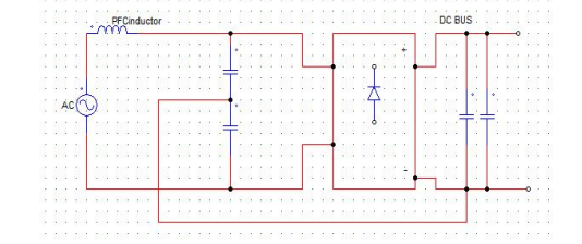
Fig: Passive PFC circuit
In this type of PFC circuits, only the passive elements are being used along with diode bridge rectifier, in order to improve of the input power factor and shape of the line current in the system. Using this PFC, input power factor of the system can be increased from the value 0.7 to 0.8 nearly. With the increase in the input voltage of the supply system, the size of circuit used for power factor correction with more components will be increased and the cost will also increase. The main objective of the PFC is, filtering input current harmonics in line current. These currents harmonics can be filtered by a using LPF and only allow the fundamental wave and stopping all the odd harmonics to improve the power factor. Using the passive PFC, current harmonics can only be decreased to a certain limits and the power factor cannot reached to a value near to unity. The output voltage cannot be controlled in this PFC circuit.
Advantages:
It is simple in structure.
It is more reliable and rugged.
Equipment’s used in passive PFC will not generate high frequency EMI
The cost required to process this method is very low.
High frequency switching losses are not present in this method and it is insensitive to noise and surges.
Disadvantages:
The size of filter will increases.
Dynamic response of the system is very low.
Output voltage control is difficult and it is not possible.
As the inductors and capacitors present in the circuit, there will be a chance of interaction between the elements in the circuit or there will be a chance to interact with the system.
With the use of filters in this method harmonics can be decreased but the fundamental component of the line current will shift its phase from the original phase.
The load connected to the system decides the shape of the input line current.
Active PFC:
An active power factor correction circuit is designed to control the power drawn by the load in the electrical system and it obtains a power factor near to unity. Any active PFC designed for power factor improvement can works as by controlling the current drawn by the load from the supply system and making it to follow the source voltage waveform. The components used in this method are to correct the shape of the input current waveform and to get the output voltage which is controllable. According to the frequency of switching the active PFC solution can be divided into two classes
- The active PFC due to low frequency: In this class switching of circuit takes at low order harmonics.
- The active PFC due to high frequency: In this class of circuit switching frequency is greater than the line-frequency
The power factor value obtained in this circuit is more than 0.9. And further the value of power factor can be increased to a higher value to reach unity can be obtained by adding some filtering elements to the circuit. With the active PFC circuit one can determine the input voltage automatically. And the size of the circuit is smaller than the one in case of passive PFC circuit. Harmonics in this case are decreased to the lower values.
Advantages:
System weight low as compared to the passive PFC circuit.
Size of the system is small and power factor value can be reached to unity approximately. Decreases the harmonics to lower values.
It will automatically corrects the AC input voltage.
It can be possible for it to operate in full rated voltage.
Disadvantages:
Design of this system is a bit complex as more number of elements are present.
Highly expensive due to its need to provide extra elements present in the circuit.
References:
- M. H. Rashid, “Power electronics: circuits, devices, and applications”, Pearson Education India, 2009.
- N. Mohan and T. M. Undeland, “Power Electronics: Converters, Applications and Design”, John Wiley & Sons, 2007.
- R. W. Erickson and D. Maksimovic, “Fundamentals of Power Electronics”, Springer Science& Business Media, 2007.
- L. Umanand, “Power Electronics: Essentials and Applications”, Wiley India, 2009.