Unit - 3
Energy – Delay Optimization
Minimum power by itself is not an interesting objective because it is achieved as the delay for a computation approaches infinity and nothing is accomplished. The time for a computation must be factored into the analysis. Better metrics include minimizing the energy, minimizing the energy-delay product, and minimizing energy under a delay constraint.
Minimum Energy
The product of the power of an operation and the time for the operation to complete is the energy consumed. Hence, the power-delay product (PDP) is simply the energy. The minimum energy point is the least energy that an operation could consume if delay were unimportant. It occurs in subthreshold operation where VDD < Vt . The minimum energy point typically consumes an order of magnitude less energy than the conventional operating point, but runs at least three orders of magnitude more slowly.
John von Neumann first asserted (without justification) that the “thermodynamic
Minimum of energy per elementary act of information” was kT ln2. Meindl proved this result for CMOS by considering the minimum allowable voltage at which an inverter could operate. To achieve nonzero noise margins, an inverter must have a slope steeper than –1 at the switching point, Vinv . For an ideal inverter with n = 1 in the subthreshold characteristics, this occurs at a minimum operating voltage of
Vmin = 2ln 2vT = 36 mV @ 300 K
The energy stored on the gate capacitance of a single MOSFET is E = QVDD/2, where Q is the charge. The minimum possible charge is one electron, q. Substituting Vmin for VDD gives Emin = kT ln 2 = 2.9 × 10⁻²¹ J. In contrast, a unit inverter in a 0.5  m 5 V process draws about 1.5 × 10⁻¹³ J from the supply when switching, and the same inverter in a 65 nm 1 V process draws 3 × 10–16 J.
Inverters have been demonstrated operating with power supplies under 100 mV, but these do not actually minimize energy in a real CMOS process. Although they have extremely low switching energy, they run so slowly that the leakage energy dominates. The true minimum energy point is at a higher voltage that balances switching and leakage energy. In subthreshold operation, the current drops exponentially as VDD – Vt decreases and Thus, the delay increases exponentially. The switching energy improves quadratically with VDD. Leakage current improves slowly with VDD because of DIBL, but the leakage energy increases exponentially because the slower gate leaks for a longer time. To achieve minimum energy operation, all transistors should be minimum width. This reduces both switching capacitance and leakage. Gate and junction leakage and short-circuit power are negligible in subthreshold operation, so the total energy is the sum of the switching and leakage energy, which is minimized near the point they crossover, as shown in Figure
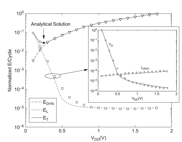
Fig 1 Minimum energy point
To compute the energy, assume that a circuit has N gates on the critical path, a total effective capacitance Ceff, and a total effective width Weff of leaking transistor. The delay of a gate operating subthreshold with a load Cg is given. The cycle time is thus

The energy consumed in one cycle is 


A more intuitive approach is to look at the minimum energy point graphically. Figure (a) plots the energy and delay contours as a function of VDD and Vt for a ring oscillator in a 180 nm process designed to reflect the behavior of a microprocessor pipeline. As VDD increases or Vt decreases, the operating frequency increases exponentially assuming the circuit is operating at or near threshold. At VDD = Vt , the circuit operates at about 10 MHz. The energy contours are normalized to the minimum energy point. This point, marked with a cross, occurs at VDD = 0.13 V and Vt = 0.37 V. The energy is about 10 times lower than at a typical operating point, but the delay is three to four orders of magnitude greater.
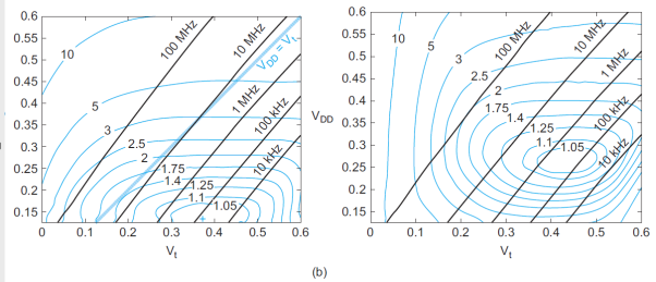
Fig 2 Contours of energy and delay rings
The shape of the curve is only a weak function of process parameters, so it remains valid for nanometer processes. However, the result does depend strongly on the relative switching and leakage energies. Figure (b) plots the results when the activity factor drops to 0.1, reducing Ceff. Switching energy is less important, so the circuit can run at a higher supply voltage. The threshold then increases to cut leakage. The total energy is greatly reduced. The result also depends on temperature: at high temperature, circuits leak more so a higher threshold voltage should be used. Process variation also pushes the best operating point toward higher voltage and energy.
Minimum Energy Delay Product
The energy-delay product (EDP) is a popular metric that balances the importance of energy and delay. Neglecting leakage, we can elegantly solve for the supply voltage that minimizes EDP. Considering leakage, the best supply voltage is slightly higher. First, consider the EDP when leakage is negligible. The energy to charge a load capacitance Ceff is given. The delay, using an α-power law model, is given. Thus, the EDP is

Differentiating with respect to VDD and setting the result to 0 gives the voltage at which
The EDP is minimized

The above equation suggests that the EDP improves as Vt approaches 0, which is obviously not true because leakage power would dominate. When a leakage term is incorporated into above equation, the results become too messy to reprint here.
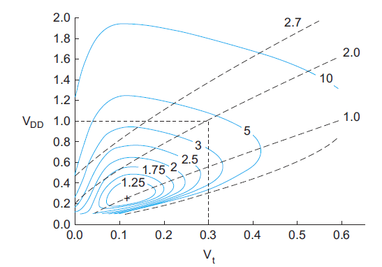
Fig 3 Contours of energy-delay product
Figure shows contours of EDP and delay as a function of VDD and Vt. EDP is normalized to the best achievable. For typical process parameters, the best Vt is about 100–150 mV and the EDP is about four times better than at a typical operating point of VDD = 1.0 V and Vt = 0.3 V. At the optimum, leakage energy is about half of dynamic energy. The dashed lines indicate contours of equal speed, normalized to the speed at the best EDP point. To operate at higher speed requires increasing the EDP.
Minimum Energy Under Delay Constraints
In practice, designers generally face the problem of achieving minimum energy under a delay constraint. Equivalently, the power consumption of the system is limited by battery or cooling considerations and the designer seeks to achieve minimum delay under an energy constraint. Figure 2(a) showed contours of delay and energy. The best supply voltage and threshold for operation at a given delay is where the delay and energy contours are tangent. For a given supply voltage and threshold voltage, the designer can make logic and sizing choices that affect delay and energy. Such curves can be generated using a logic synthesizer or sizing tool constrained to various delays. The curve becomes steep near the point of minimum delay, so energy-efficient designs should aim to operate at a longer delay. Energy under a delay constraint is also minimized when leakage is about half of dynamic power. However, the curve is fairly flat around this point, so many designs operate at lower leakage to facilitate power saving during sleep mode.
Key takeaway
Minimum power by itself is not an interesting objective because it is achieved as the delay for a computation approaches infinity and nothing is accomplished. The time for a computation must be factored into the analysis. Better metrics include minimizing the energy, minimizing the energy-delay product, and minimizing energy under a delay constraint.
Microarchitecture
Energy-efficient architectures take advantage of the structured design principles of modularity and locality observed that processor performance grows with the square root of the number of transistors. Building complex, sprawling processors to extract the last bit of instruction-level parallelism from a problem is a highly inefficient use of energy. Microarchitectures are moving toward larger numbers of simpler cores seeking to handle task and data-level parallelism. Smaller cores also have shorter wires and faster memory access. Memories have a much lower power density than logic because their activity factors are miniscule and their regularity simplifies leakage control.
If a task can be accelerated using either a faster processor or a larger memory, the memory is often preferable. Memories now comprise more than half the area of many chips. Special-purpose functional units can offer an order of magnitude better energy efficiency than general-purpose processors. Accelerators for compute-intensive applications such as graphics, networking, and cryptography offload these tasks from the processor. Such heterogeneous architectures, combining regular cores, specialized accelerators, and large amounts of memory, are of growing importance.
Commercial software has historically lagged at least a decade behind hardware advances such as virtual memory, memory protection, 32- and 64-bit datapaths, and robust power-management. Presently, programmers have trouble taking advantage of many cores. Time will tell whether programming practices and tools catch up or whether microarchitectures will have to yield to the needs of programmers.
Parallelism and Piping
In the past, parallelism and pipelining have been effective ways to reduce power consumption, as shown in Figure. Replacing a single functional unit with N parallel units allows each to operate at 1/N the frequency. A multiplexer selects between the results. The voltage can be scaled down accordingly, offering quadratic savings in energy at the expense of doubling the area. Replacing a single functional unit with an N-stage pipelined unit also reduces the amount of logic in a clock cycle at the expense of more registers. Again, the voltage can be scaled down. The two techniques can be combined for even better energy efficiency.
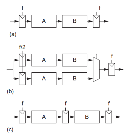
Fig 4 Functional units: (a) normal, (b) parallel, (c) pipelined
When leakage is unimportant, parallelism offers a slight edge because the multiplexer has less overhead than the pipeline registers. Also, perfectly balancing logic across pipeline stages can be difficult. Now that leakage is a substantial fraction of total power, pipelining becomes preferable because the parallel hardware has N times as much leakage. Now that VDD is closer to the best energy-delay point, the potential supply reduction and energy savings are diminishing. Nevertheless, parallelism and pipelining remain primary tools to extract performance from the vast transistor budgets now available.
Power Management Modes
Chip designers have now learned they must turn off portions of the chip when they are not active by applying clock and power gating. Many chips now employ a variety of power management modes giving a trade-off between power savings and wake-up time. For example, the Intel Atom processor operates at a peak frequency of 2 GHz at 1 V, consuming 2 W. The power management modes are shown in Figure.
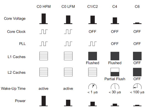
Fig 5 Atom power management modes
In the low frequency mode, the clock drops as slow as 600 MHz while the power supply. Reduces to 0.75 V. In sleep mode C1, the core clock is turned off and the level 1 cache is flushed and power-gated to reduce leakage, but the processor can return to active state in 1 microsecond. In sleep mode C4, the PLL is also turned OFF. In sleep mode C6, the core and caches are all power-gated to reduce power to less than 80 mW, but wake-up time rises to 100 microseconds. For a typical workload, the processor can spend 80–90% of its time in C6 sleep mode, reducing average power to 220 mW.
The worst-case power that a chip may consume can be a factor of two or more greater than the normal power. Code triggering maximal power consumption is sometimes called a thermal virus because it seeks to burn out the chip. To avoid having to design for this worst case, chips can employ adaptive features, throttling back activity if the issue rate or die temperature becomes too high. Power management results in substantially lower power consumption during idle mode than active mode. The transition between idle and active may require multiple cycles to avoid sudden current spikes that excite power supply resonances and cause excessive supply noise.
Key takeaway
Energy-efficient architectures take advantage of the structured design principles of modularity and locality observed that processor performance grows with the square root of the number of transistors. Building complex, sprawling processors to extract the last bit of instruction-level parallelism from a problem is a highly inefficient use of energy.
The wires linking transistors together are called interconnect and play a major role in the performance of modern systems. In the early days of VLSI, transistors were relatively slow. Wires were wide and thick and thus had low resistance. Under those circumstances, wires could be treated as ideal equipotential nodes with lumped capacitance. In modern VLSI processes, transistors switch much faster. Meanwhile, wires have become narrower, driving up their resistance to the point, that in many signal paths, the wire RC delay exceeds gate delay. Moreover, the wires are packed very closely together and thus a large fraction of their capacitance is to their neighbors. When one wire switches, it tends to affect its neighbor through capacitive coupling; this effect is called crosstalk. Wires also account for a large portion of the switching energy of a chip. On-chip interconnect inductance had been negligible but is now becoming a factor for systems with fast edge rates and closely packed busses. Considering all of these factors, circuit design is now as much about engineering the wires as the transistors that sit underneath.
Figure shows a pair of adjacent wires. The wires have width w, length l, thickness t, and spacing of s from their neighbors and have a dielectric of height h between them and the conducting layer below. The sum of width and spacing is called the wire pitch. The thickness to width ratio t/w is called the aspect ratio.
Early CMOS processes had a single metal layer and until the early 1990s only two or three layers were available, but with advances in chemical mechanical polishing it became far more practical to manufacture many metal layers. As aluminium (Al) wires used in older processes gave way to copper (Cu) around the 180 or 130 nm node to reduce resistance. Soon after, manufacturers began replacing the SiO2 insulator between wires with a succession of materials with lower dielectric constants (low-k) to reduce capacitance.
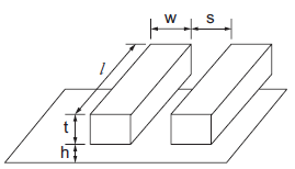
Fig 6 Interconnect Geometry
A 65 nm process typically has 8–10 metal layers and the layer count has been increasing at a rate of about one layer every process generation or two.
A pipe makes a good mechanical analogy for a wire, as shown in Figure below. The resistance relates to the wires cross-sectional area. A narrow pipe impedes the flow of current. The capacitance relates to a trough underneath the leaky pipe that must fill up before current passes out the end of the pipe. And the inductance relates to a paddle wheel along the wire with inertia that opposes changes in the rate of flow. Each of these elements is discussed further in this section. A wire is a distributed circuit with a resistance and capacitance per unit length. Its behavior can be approximated with a number of lumped elements. Three standard approximations are the L-model, π -model, and T-model, so-named because of their shapes.
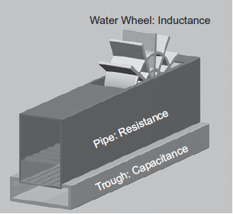
Fig 7 Pipe Analogy for wire
Figure below shows how a distributed RC circuit is equivalent to N distributed RC segments of proportionally smaller resistance and capacitance, and how these segments can be modeled with lumped elements. As the number of segments approaches infinity, the lumped approximation will converge with the true distributed circuit. The L-model is a poor choice because a large number of segments are required for accurate results. The π-model is much better; three segments are sufficient to give results accurate to 3%. The T-model is comparable to the π -model, but produces a circuit with one more node that is slower to solve by hand or with a circuit simulator. Therefore, it is common practice to model long wires with a 3–5 segment π -model for simulation. If inductance is considered, it is placed in series with each resistor.
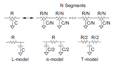
Fig 8 Lumped Approximation to distributes RC Circuit
Resistance
The resistance of a uniform slab of conducting material can be expressed as


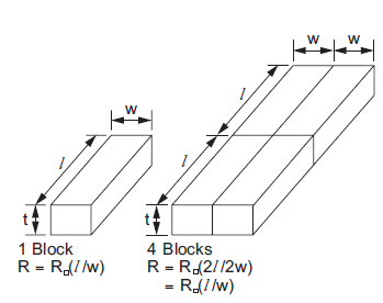
Fig 9 Two conductors with equal resistance
R0 =  /t
/t
 = resistivity
To obtain the resistance of a conductor on a layer, multiply the sheet resistance by the ratio of length to width of the conductor. For example, the resistances of the two shapes in Figure above are equal because the length-to-width ratio is the same even though the sizes are different. Nonrectangular shapes can be decomposed into simpler regions for which the resistance is calculated.
Table shows bulk electrical resistivities of pure metals at room temperature
Metal | Resistivity( cm) |
Silver (Ag) | 1.6 |
Copper (Cu) | 1.7 |
Gold(Au) | 2.2 |
Aluminium(Al) | 2.8 |
Molybdenum (Mo) | 5.3 |
Tungsten(W) | 5.3 |
Titanium(Ti) | 43.0 |
As shown in Figure below, copper must be surrounded by a lower-conductivity diffusion barrier that effectively reduces the wire cross-sectional area and hence raises the resistance. Moreover, the polishing step can cause dishing that thins the metal. Even a 10 nm barrier is quite significant when the wire width is only tens of nanometers. If the average barrier thickness is t barrier and the height is reduced by tdish, the resistance becomes 

Fig 10 Copper Barrier Layer and Dishing
The resistivity of polysilicon, diffusion, and wells is significantly influenced by the doping levels. Polysilicon and diffusion typically have sheet resistances under 10  /square when silicided and up to several hundred /square when unsilicided. Wells have lower doping and thus even higher sheet resistance. These numbers are highly process dependent. Large resistors are often made from wells or unsilicided polysilicon.

Fig 11 Multiple vias for low resistance connection
Multiple contacts should be used to form low-resistance connections, as shown in Figure above. When current turns at a right angle or reverses, a square array of contacts is generally required, while fewer contacts can be used when the flow is in the same direction.
Example
Compute the sheet resistance of a 0.22 m thick Cu wire in a 65 mm process. Find the total resistance if the wire is 0.125m wide and 1 mm long. Ignore the barrier layer and dishing.
Solution:
The sheet resistance is

The total resistance is

An isolated wire over the substrate can be modelled as a conductor over a ground plane. The wire capacitance has two major components: the parallel plate capacitance of the bottom of the wire to ground and the fringing capacitance arising from fringing fields along the edge of a conductor with finite thickness. In addition, a wire adjacent to a second wire on the same layer can exhibit capacitance to that neighbor. These effects are illustrated in Figure below. The classic parallel plate capacitance formula is


Fig 12 Effect of fringing fields on capacitance
The fringing capacitance is more complicated to compute and requires a numerical field solver for exact results. Two hemispherical end caps, as shown in Figure below. The total capacitance is assumed to be the sum of a parallel plate capacitor of width w – t/2 and a cylindrical capacitor of radius t/2. This results in an expression for the capacitance that is accurate within 10% for aspect ratios less than 2 and t =h.
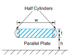
Fig 13 Capacitance model including fringing


These formulae do not account for neighbors on the same layer or higher layers. Capacitance interactions between layers can become quite complex in modern multilayer CMOS processes. A conservative upper bound on capacitance can be obtained assuming parallel neighbors on the same layer at minimum spacing and that the layers above and below the conductor of interest are solid ground planes. Similarly, a lower bound can be obtained assuming there are no other conductors in the system except the substrate. The upper bound can be used for propagation delay and power estimation while the lower bound can be used for contamination delay calculations before layout information is available.
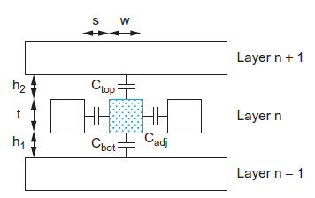
Fig 14 Multilayer capacitance model
A cross-section of the model used for capacitance upper bound calculations is shown in Figure above. The total capacitance of the conductor of interest is the sum of its capacitance to the layer above, the layer below, and the two adjacent conductors. If the layers above and below are not switching, they can be modeled as ground planes and this component of capacitance is called Cgnd. Wires do have some capacitance to further neighbors, but this capacitance is generally negligible because most electric fields terminate on the nearest conductors. The dielectrics used between adjacent wires have the lowest possible dielectric constant khoriz to minimize capacitance. The dielectric between layers must provide greater mechanical stability and may have a larger kvert. The constant Cfringe term accounts for fringing capacitance and gives a better fit for w and s up to several times minimum


Inductance
Most design tools consider only interconnect resistance and capacitance. Inductance is difficult to extract and model, so engineers prefer to design in such a way that inductive effects are negligible. Nevertheless, inductance needs to be considered in high-speed designs for wide wires such as clocks and power busses.
Although we generally discuss current flowing from a gate output to charge or discharge a load capacitance, current really flows in loops. The return path for a current loop is usually the power or ground network; at the frequencies of interest, the power supply is an “AC ground” because the bypass capacitance forms a low-impedance path between VDD and GND. Currents flowing around a loop generate a magnetic field proportional to the area of the loop and the amount of current. Changing the current requires supplying energy to change the magnetic field. This means that changing currents induce a voltage proportional to the rate of change. The constant of proportionality is called the inductance, L.

Inductance and capacitance also set the speed of light in a medium. Even if the resistance of a wire is zero leading to zero RC delay, the speed of light flight-time along a wire of length with inductance and capacitance per unit length of L and C is

If the current return paths are the same as the conductors on which electric field lines terminate, the signal velocity v is

Where  0 is the magnetic permeability of free space (4π × 10–7 H/m) and c is the speed of light in free space (3 × 10⁸ m/s). In other words, signals travel about half the speed of light. Using low-k (< 3.9) dielectrics raises this velocity. However, many signals have electric fields terminating on nearby neighbors, but currents returning in more distant power supply lines. This raises the inductance and reduces the signal velocity. Changing magnetic fields in turn produce currents in other loops. Hence, signals on one wire can inductively couple onto another; this is called inductive crosstalk.
The inductance of a conductor of length l and width w located a height h above a ground plane is approximately

Extracting inductance in general is a three-dimensional problem and is extremely time consuming for complex geometries. Inductance depends on the entire loop and therefore cannot be simply decomposed into sections as with capacitance. It is therefore impractical to extract the inductance from a chip layout.
Skin Effect
Current flows along the path of lowest impedance Z = R + jωL. At high frequency, ω impedance becomes dominated by inductance. The inductance is minimized if the current flows only near the surface of the conductor closest to the return path(s). This skin effect can reduce the effective cross-sectional area of thick conductors and raise the effective resistance at high frequency. The skin depth for a conductor is

Where  is the magnetic permeability of the dielectric (normally the same as in free space, 4π × 10–7 H/m). The frequency of importance is the highest frequency with significant power in the Fourier transform of the signal. This is not the chip operating frequency, but rather is associated with the faster edges. A sine wave with the same 20–80% rise/fall time as the signal has a period of 8.65trf. Therefore, the frequency associated with the edge can be approximated as

In a chip with a good power grid, good current return paths are usually available on all sides. Thus, it is a reasonable approximation to assume the current flows in a shell of thickness  along the four sides of the conductor, as shown in Figure below. If min(w, t) > 2
  , part of the conductor carries no current and the resistance increases.
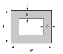
Fig 15 Current flow in shell determined by skin depth
Example
Q) Determine the skin depth for a copper wire in a chip with 20 ps edge rates.
A) The maximum frequency of interest is


The skin depth will then be calculated as

Temperature Dependence
Interconnect capacitance is independent of temperature, but the resistance varies strongly. The temperature coefficients of copper and aluminum are about 0.4%/°Cover the normal operating range of circuits; that is, a 100 °C increase in temperature leads to 40% higher resistance. At liquid nitrogen temperature (77 K), the resistivity of copper drops to 0.22  · cm, an order-of-magnitude improvement. This suggests great advantages for RC dominated paths in cooled systems.
Key takeaway
A wire is a distributed circuit with a resistance and capacitance per unit length. Its behavior can be approximated with a number of lumped elements. Three standard approximations are the L-model, π -model, and T-model, so-named because of their shapes.
Delay
Interconnect increases circuit delay for two reasons. First, the wire capacitance adds loading to each gate. Second, long wires have significant resistance that contributes distributed RC delay or flight time. The Elmore delay of a single-segment L-model is RC. As the number of segments of the L-model increases, the Elmore delay decreases toward RC/2. The Elmore delay of a π- or T model is RC/2 no matter how many segments are used. Thus, a single-segment π-model is a good approximation for hand calculations.
Example
Q) 10x unit-sized inverter drives a 2x inverter at the end of the 1mm wire from Example. Suppose that wire capacitance is 0.2 fF/m and that unit-sized nMOS transistor has R10k and C=0.1Ff. Estimate the propagation delay using the Elmore delay model; neglect diffusion capacitance.
A) The driver has a resistance of 1k. The receiver has a 2-Unit nMOS transistor and a 4-unit pMOS transistor, for a capacitance of 0.6Ff. The wire capacitance is 200Ff.
Figure shows an equivalent circuit for the system using a single-segment π-model. The Elmore delay is  The capacitance of the long wire dominates the delay; the capacitance of the 2x inverter is negligible in comparison.

Because both wire resistance and wire capacitance increase with length, wire delay grows quadratically with length. Using thicker and wider wires, lower-resistance metals such as copper, and lower-dielectric constant insulators helps, but long wires nevertheless often have unacceptable delay.
Q) Find RC flight time per  for a wire using the parameters form example above express the result in FO4
 , if the FO4 inverter delay is 15ps. What is the flight time to cross a 10mm die?
A)
R=800/mm, C=0.2 pF/mm. The flight time is RC/2=80ps/ ,or 5.3 FO
 . The flight time across a 10mm die is thus 530 FO4, which is dozens of clock cycles.
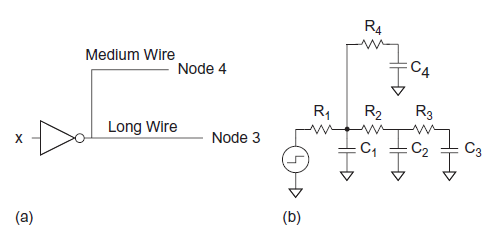
Q) Figure models a gate driving wires to destinations. The gate is represented as a voltage source with effective resistance  . The two receivers are located at nodes 3 and 4. The wire to node 3 is long enough that it is represented with a pair of π-segments, while the wire to node 4 is representation with a single segment. Find the Elmore delay from input x to each receiver.
A)
The elmore delays are


Energy
The switching energy of a wire is set by its capacitance. Long wires have significant capacitance and thus require substantial amounts of energy to switch.
Example
Q) Estimate the energy per unit length to send a bit of information (one rising and one falling transition) in a CMOS process.
A)
E = (0.2 pF/mm) (1.0 V)2 = 0.2 pJ/bit/mm. Sometimes energy in a communication link is expressed as power per gigabit per second: 0.2 mW/Gbps.
Q) Consider a microprocessor on a 20 mm × 20 mm die running at 3 GHz in the 65 nm process. A layer of metal is routed on a 250 nm pitch. Half of the available wire tracks are used. The wires have an average activity factor of 0.1. Determine the power consumed by the layer of metal.
A) There are (20 mm) / (250 nm) = 80,000 tracks of metal across the die, of which 40,000 are occupied. The wire capacitance is (0.2 pF/mm)(20 mm)(40,000 tracks) = 160 nF. The power is (0.1)(160 nF)(1.0 V)2(3 GHz) = 48 W. This is clearly a problem, especially considering that the chip has more than one layer of metal. The activity factor needs to be much lower to keep power under control.
Cross talk
When wire A switches, it tends to bring its neighbor B along with it on account of capacitive coupling, also called crosstalk. If B is supposed to switch simultaneously, this may increase or decrease the switching delay. If B is not supposed to switch, crosstalk causes noise on B. We will see that the impact of crosstalk depends on the ratio of Cadj to the total capacitance. Note that the load capacitance is included in the total, so for short wires and large loads, the load capacitance dominates and crosstalk is unimportant. Conversely, crosstalk is very important for long wires.
Crosstalk Delay Effects
If both a wire and its neighbor are switching, the direction of the switching affects the amount of charge that must be delivered and the delay of the switching. Table summarizes this effect. The charge delivered to the coupling capacitor is Q = Cadj  V, where
  V is the change in voltage between A and B. If A switches but B does not,
  V = VDD. The total capacitance effectively seen by A is just the capacitance to ground and to B. If both A and B switch in the same direction,
  = 0. Hence, no charge is required and Cadj is effectively absent for delay purposes. If A and B switch in the opposite direction,
  V = 2VDD. Twice as much charge is required. Equivalently, the capacitor can be treated as being effectively twice as large switching through VDD. This is analogous to the Miller effect discussed in Section 4.4.6.6. The Miller Coupling Factor (MCF) describes how the capacitance to adjacent wires is multiplied to find the effective capacitance.
Some designers use MCF = 1.5 as a statistical compromise when estimating propagation delays before layout information is available.
B | V |  | MCF |
Constant |
 |  | 1 |
Switching same direction as A | 0 |  | 0 |
Switching opposite to A |  |  | 2 |
Example
Q) Each wire in a pair of 1 mm lines has capacitance of 0.08 fF/m to ground and 0.12 fF/ m to its neighbor. Each line is driven by an inverter with a 1 k effective resistance.
Estimate the contamination and propagation delays of the path. Neglect parasitic capacitance of the inverter and resistance of the wires.
A) We find Cgnd = (0.08 fF/ m) (1000
  m) = 80 fF and Cadj = 120 fF. The delay is RCeff. The contamination delay is the minimum possible delay, which occurs when both wires switch in the same direction.
In that case, Ceff = Cgnd and the delay is tcd = (1 k )(0.08 pF) = 80 ps. The propagation delay is the maximum possible delay, which occurs when both wires switch in opposite directions.
In this case, Ceff = Cgnd + 2Cadj and the delay is tpd = (1 k )(0.32 pF) = 320 ps. This is a factor of four difference between best and worst case.
Crosstalk Noise Effects
Suppose wire A switches while B is supposed to remain constant. This introduces noise as B partially switches. We call A the aggressor or perpetrator and B the victim. If the victim is floating, we can model the circuit as a capacitive voltage divider to compute the victim noise, as shown in Figure below  Vaggressor is normally VDD

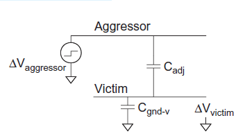
Fig 16 Coupling to floating victim
If the victim is actively driven, the driver will supply current to oppose and reduce the victim noise. We model the drivers as resistors, as shown in Figure below. The peak noise becomes dependent on the time constant ratio k of the aggressor to the victim.
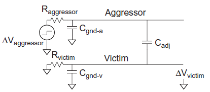
Fig 17 Coupling to driven victim


Inductive Effects
Inductance has always been important for integrated circuit packages where the physical dimensions are large. On-chip inductance is important for wires where the speed-of-light flight time is longer than either the rise times of the circuits or the RC delay of the wire. Because speed-of-light flight time increases link and RC delay increases quadratically with length, we can estimate the set of wire lengths for which inductance is relevant

Effective Resistance and Elmore Delay
According to the Elmore delay model, a gate with effective resistance R and capacitance C has a propagation delay of RC. A wire with distributed resistance R and capacitance C treated as a single π-segment has propagation delay RC/2. Reviewing the properties of RC circuits, we recall that the lumped RC circuit in Figure (a) has a unit step response of

The propagation delay of this circuit is obtained by solving for tpd when Vout(tpd) = 1/2:

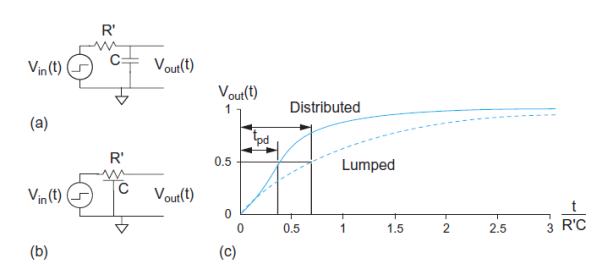
Fig 18 Lumped and Distributed RC circuit Response
The distributed RC circuit in Figure (b) has no closed form time domain response. Because the capacitance is distributed along the circuit rather than all being at the end, you would expect the capacitance to be charged on average through about half the resistance and that the propagation delay should thus be about half as great. A numerical analysis finds that the propagation delay is 0.38R’C.
The Elmore model with the true results for a logic gate, recall that logic gates have complex nonlinear I-V characteristics and are approximated as having an effective resistance. If we characterize that effective resistance as R = R’ ln 2, the propagation delay really becomes the product of the effective resistance and the capacitance: tpd = RC.
For distributed circuits, observe that
0.38 R’C = (1/2) R’C ln 2 = RC/2
Therefore, the Elmore delay model describes distributed delay well if we use an effective wire resistance scaled by ln 2. This suggests that when the input is slow, the effective resistance for delay calculations in a distributed RC circuit is equal to the true resistance.
Key takeaway
Interconnect increases circuit delay for two reasons. First, the wire capacitance adds loading to each gate. Second, long wires have significant resistance that contributes distributed RC delay or flight time. The Elmore delay of a single-segment L-model is RC. As the number of segments of the L-model increases, the Elmore delay decreases toward RC/2. The Elmore delay of a π- or T model is RC/2 no matter how many segments are used. Thus, a single-segment π-model is a good approximation for hand calculations.
As gate delays continue to improve while long wire delays remain constant or even get slower, wire engineering has become a major part of integrated circuit design. It is necessary to develop a floorplan early in the design cycle, identify the long wires, and plan for them. While floor planning in such a way that critical communicating units are close to one another has the greatest impact on performance, it is inevitable that long wires will still exist. Aspect ratios in old processes were below 1, but are close to 2 in nano meter processes to help the resistance of such narrow lines. This comes at the expense of substantially increased coupling capacitance.
The designer has a number of techniques to engineer wires for delay and coupling noise. The width, spacing, and layer usage are all under the designer’s control. Shielding can be used to further reduce coupling on critical nets. Repeaters inserted along long wires reduce the delay from a quadratic to a linear function of length. Wire capacitance and resistance complicate the use of Logical Effort in selecting gate sizes.
Width, Spacing and Layer
The designer selects the wire width, spacing, and layer usage to trade off delay, bandwidth, energy, and noise. By default, minimum pitch wires are preferred for noncritical interconnections for best density and bandwidth. When the load is dominated by wire capacitance, the best way to reduce delay is to increase spacing, reducing the capacitance to nearby neighbors. This also reduces energy and coupling noise. When the delay is dominated by the gate capacitance and wire resistance, widening the wire reduces resistance and delay.
However, it increases the capacitance of the top and bottom plates. Widening wires also increases the fraction of capacitance of the top and bottom plates, which somewhat reduces coupling noise from adjacent wires. However, wider wires consume more energy. The wire thickness depends on the choice of metal layer. The lower layers are thin and optimized for a tight routing pitch. Middle layers are often slightly thicker for lower resistance and better current-handling capability. Upper layers may be even thicker to provide a low-resistance power grid and fast global interconnect. Wiring tracks are a precious resource and are often allocated in the floorplan; the wise designer maintains a reserve of wiring tracks for unanticipated changes late in the design process. The power grid is usually distributed over multiple layers. Most of the current handling capability is provided in the upper two layers with lowest resistance. However, the grid must extend down to metal1 or metal2 to provide easy connection to cells.
Repeaters
Both resistance and capacitance increase with wire length l, so the RC delay of a wire increases with l2, as shown in Figure (a). The delay may be reduced by splitting the wire into N segments and inserting an inverter or buffer called a repeater to actively drive the wire, as shown in Figure (b). The new wire involves N segments with RC flight time of (l/N)2, for a total delay of l2 /N. If the number of segments is proportional to the length, the overall delay increases only linearly with l.
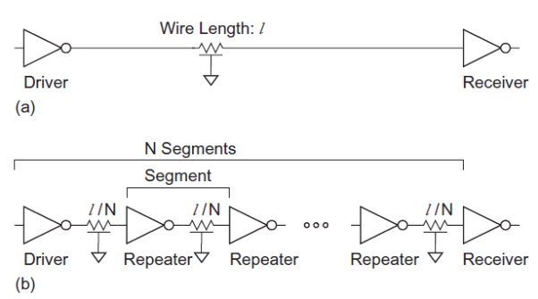
Fig 19 Wire with and without repeaters
Using inverters as repeaters gives best performance. Each repeater adds some delay. If the distance is too great between repeaters, the delay will be dominated by the long wires. If the distance is too small, the delay will be dominated by the large number of inverters. As usual, the best distance between repeaters is a compromise between these extremes. Suppose a unit inverter has resistance R, gate capacitance C and diffusion capacitance Cpinv. A wire has resistance Rw and capacitance Cw per unit length. Consider inserting repeaters of W times unit size.
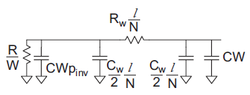
Fig 20 Equivalent circuit for segment of repeated wire
Figure above shows a model of one segment. The Elmore delay of the repeated wire is

Differentiating above equation w.r.t W and N we get

Assuming pinv = 0.5

The delay per unit length of a properly repeated wire is

To achieve this delay, the inverters should use an nMOS transistor width of

The energy per unit length to send a bit depends on the wire and repeater capacitances

In other words, repeaters sized for minimum delay add 87% to the energy of an unrepeated wire.
Example
Q) Compute the delay per mm of a repeated wire in a 65 nm process. Assume the wire is on a middle routing layer and has 2x width, spacing, and height, so its resistance is 200  /mm and capacitance is 0.2 pF/mm. The FO4 inverter delay is 15 ps. Also find the repeater spacing and driver size to achieve this delay and the energy per bit.
A) The delay is

This delay is achieved using a spacing of 0.45 mm between repeaters and an nMOS
Driver width of 18  m (180x unit size). The energy per bit is 0.4 pJ/mm.
Cross talk Control
The capacitive crosstalk is proportional to the ratio of coupling capacitance to total capacitance. For modern wires with an aspect ratio (t/w) of 2 or greater, the coupling capacitance can account for 2/3 to 3/4 of the total capacitance and crosstalk can create large amounts of noise and huge data-dependent delay variations.
There are several approaches to controlling this crosstalk:
_ Increase spacing to adjacent lines
_ Shield wires
_ Ensure neighbors switch at different times
_ Crosstalk cancellation
The easiest approach to fix a minor crosstalk problem is to increase the spacing. If the crosstalk is severe, the spacing may have to be increased by more than one full track. In such a case, it is more efficient to shield critical signals with power or ground wires on one or both sides to eliminate coupling. For example, clock wires are usually shielded so that switching neighbors do not affect the delay of the clock wire and introduce clock jitter.
Sensitive analog wires passing near digital signals should also be shielded. An alternative to shielding is to interleave busses that are guaranteed to switch at different times. For example, if bus A switches on the rising edge of the clock and bus B switches on the falling edge of the clock, by interleaving the bits of the two busses you can guarantee that both neighbors are constant during a switching event. This avoids the delay impact of coupling; however, you must still ensure that coupling noise does not exceed noise budgets. Figure below shows wires shielded (a) on one side, (b) on both sides, and (c) interleaved. Critical signals such as clocks or analog voltages can be shielded above and below as well.

Fig 21 Wire Shielding Topologies
Alternatively, wires can be arranged to cancel the effects of crosstalk. Three such methods include staggered repeaters, charge compensation, and twisted differential signaling. Each technique seeks to cause equal amounts of positive and negative crosstalk on the victim, effectively producing zero net crosstalk.
Figure (a) below shows two wires with staggered repeaters. Each segment of the victim sees half of a rising aggressor segment and half of a falling aggressor segment. Although the cancellation is not perfect because of delays along the segments, staggering is a very effective approach. Figure (b) below shows charge compensation in which an inverter and transistor are added between the aggressor and victim. The transistor is connected to behave as a capacitor. When the aggressor rises and couples the victim upward, the inverter falls and couples the victim downward. By choosing an appropriately sized compensation transistor, most of the noise can be cancelled at the expense of the extra circuitry. Figure (c) shows twisted differential signaling in which each signal is routed differentially. The signals are swapped or twisted such that the victim and its complement each see equal coupling from the aggressor and its complement. This approach is expensive in wiring resources, but it effectively eliminates crosstalk.
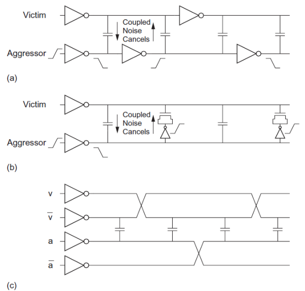
Fig 22 Cross talk Control Scheme
Regenerators
Repeaters are placed in series with wires and thus are limited to unidirectional busses. An alternative is to use regenerators (also called boosters) placed in parallel with wires at periodic intervals, as shown in Figure below. When the wire is initially ‘0,’ the regenerator senses a rising transition and accelerates it. Conversely, when the wire is initially ‘1,’ the regenerator accelerates the falling transition. Regenerators trade off up to 20% better delay or energy for reduced noise margins.
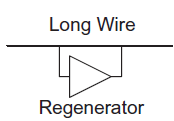
Fig 23 Regenerator
Figure below shows a self-timed regenerator. When the wire begins to rise, the LO-skewed NAND gate detects the transition midway and turns on the pMOS driver to assist. The normal skew inverters eventually detect the transition and flip node x, turning off the pMOS driver. When the wire begins to fall, the HI-skewed NOR gate turns on the nMOS to assist.
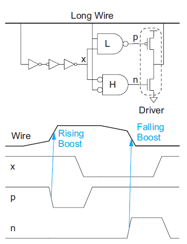
Fig 24 Regenerator
Key takeaway
The capacitive crosstalk is proportional to the ratio of coupling capacitance to total capacitance. For modern wires with an aspect ratio (t/w) of 2 or greater, the coupling capacitance can account for 2/3 to 3/4 of the total capacitance and crosstalk can create large amounts of noise and huge data-dependent delay variations.
There are several approaches to controlling this crosstalk:
_ Increase spacing to adjacent lines
_ Shield wires
_ Ensure neighbors switch at different times
_ Crosstalk cancellation
Interconnect complicates the application of Logical Effort because the wires have a fixed capacitance. The branching effort at a wire with capacitance Cwire driving a gate load of Cgate is (Cgate + Cwire) / Cgate. This branching effort is not constant; it depends on the size of the gate being driven. The simple rule that circuits are fastest when all stages bear equal effort is no longer true when wire capacitance is introduced. If the wire is very short or very long, approximations are possible, but when the wire and gate loads are comparable, there is no simple method to determine the best stage effort.
Every circuit has some interconnect, but when the interconnect is short (Cwire << Cgate), it can be ignored. Alternatively, you can compute the average ratio of wire capacitance to parasitic diffusion capacitance and add this as extra parasitic capacitance when determining parasitic delay. For connections between nearby gates, this generally leads to a best stage effort  slightly greater than 4. The path should use fewer stages because each stage contributes wire capacitance. To reduce delay, the gates should be sized larger so that the wire capacitance is a smaller fraction of the whole. However, this comes at the expense of increased energy.
Conversely, when the interconnect is long (Cwire >> Cgate), the gate at the end can be ignored. The path can now be partitioned into two parts. The first part drives the wire while the second receives its input from the wire. The first part is designed to drive the load capacitance of the wire; the extra load of the receiver is negligible. To save energy, the final stage driving the wire should have a low logical effort and a high electrical effort; an inverter is preferred. The size of the receiver is chosen by practical considerations: Larger receivers may be faster, but they also cost area and power. If the wire is long enough that the RC flight time exceeds a few gate delays, it should be broken into segments driven by repeaters.
The most difficult problems occur when Cwire Cgate. These medium-length wires introduce branching efforts that are a strong function of the size of the gates they drive. Writing a delay equation as a function of the gate sizes along the path and the wire capacitance results in an expression that can be differentiated with respect to gate sizes to compute the best sizes.

Fig 25 Path with wires
Alternatively, a convex optimizer can be used to minimize delay or generate an energy-delay trade-off curve. Figure above shows three stages along a path. By writing the Elmore delay and differentiating with respect to the size of the middle stage, we find the interesting result that the delay caused by the capacitance of a stage should equal the delay caused by the resistance of the stage.
Example The path in figure contains a medium-length wire modelled as a lumped capacitance. Write an equation for path delay in terms of x and y. How large should the x and y inverters be for shortest path delay? What is the stage effort of each stage?
Solution:
From the logical effort delay model, we find the path delay is

Differentiating with respect to each size and setting the results to 0 allows us tosolve Eq(6.41) for x=33fF and y=57fF.


The stage efforts are (33/10)=3.3, (57+50)/33=3/2 and (100/57)=1.8. Notice that the first two stage efforts are equal as usual, but the third stage effort is lower. As x already drives a large wire capacitance, y may be rather large(and will bear a small stage effort) before the incremental increase in delay of x driving y equals the incremental decreases in delay of y driving the output.
References:
1. D. A. Pucknell and K. Eshraghian, “Basic VLSI Design: Systems and Circuits”, PHI, 3rd Ed.,1994.
2. W.Wolf, Modern VLSI Design: System on Chip, Third Edition, Pearson, 2002.