Unit - 4
Dynamic logic circuits
- Wide range of static combinational and sequential logic circuits was introduced in the previous chapters.
- Static logic circuits allow versatile implementation of logic functions based on static, or steady-state, behavior of simple nMOS or CMOS structures.
- In other words, all valid output levels in static gates are associated with steady-state operating points of the circuit in question.
- Hence, a typical static logic gate generates its output corresponding to the applied input voltages after a certain time delay, and it can preserve its output level (or state) as long as the power supply is provided.
- This approach, however, may require a large number of transistors to implement a function, and may cause a considerable time delay.
- In high-density, high-performance digital implementations where reduction of circuit delay and silicon area is a major objective, dynamic logic circuits offer several significant advantages over static logic circuits.
- The operation of all dynamic logic gates depends on temporary (transient) storage of charge in parasitic node capacitances, instead of relying on steady-state circuit behavior.
- This operational property necessitates periodic updating of internal node voltage levels, since stored charge in a capacitor cannot be retained indefinitely.
- Consequently, dynamic logic circuits require periodic clock signals in order to control charge refreshing.
- The capability of temporarily storing a state, i.e., a voltage level, at a capacitive node allows us to implement very simple sequential circuits with memory functions.
- The use of common clock signals throughout the system enables us to synchronize the operations of various circuit blocks.
- Dynamic circuit techniques lend themselves well to synchronous logic design.
- Finally, the dynamic logic implementation of complex functions generally requires a smaller silicon area than does the static logic implementation.
- As for the power consumption which increases with the parasitic capacitances, the dynamic circuit implementation in a smaller area will, in many cases, consume less power than the static counterpart, despite its use of clock signals.
Example
Consider the dynamic D-latch circuit shown below. The circuit consists of two cascaded inverters and one nMOS pass transistor driving the input of the primary inverter stage.

Sol: We will see that the parasitic input capacitance C. Of the primary inverter stage plays an important role in the dynamic operation of this circuit. The input pass transistor is being driven by the external periodic clock signal, as follows:
- When the clock is high (CK = 1), the pass transistor turns on. The capacitor C, is either charged up, or charged down through the pass transistor MP, depending on the input (D) voltage level. The output (Q) assumes the same logic level as the input.
- When the clock is low (CK = 0), the pass transistor MP turns off, and the capacitor C is isolated from the input D. Since there is no current path from the intermediate node X to either VDD or ground, the amount of charge stored in C. During the previous cycle determines the output voltage level Q.
It can easily be seen that this circuit performs the function of a simple D-latch. In fact, the transistor count can be reduced by removing the last inverter stage if the latch output can be inverted. This option will be elaborated on in next section. The "hold" operation during the inactive clock cycle is accomplished by temporarily storing charge in the parasitic capacitance C. Correct operation of the circuit critically depends on how long a sufficient amount of charge can be retained at node X, before the output state changes due to charge leakage. Therefore, the capacitive intermediate node X is also called a soft node. The nature of the soft node makes the dynamic circuits more vulnerable to the so called single-event upsets (SEUs) caused by a-particle or cosmic ray hits in integrated circuits.
In the following, we will examine the circuit operation in more detail. Assume that the dynamic D-latch circuit is being operated with a power supply voltage of VDD = V, and that the VTC of both inverters are identical, with VOL = 0V
VIL= 2 .1 V
VIH =2.9 V
VOH = 5.0 V
Furthermore, the threshold voltage of the pass transistor MP is given as VT = 0.8 V. During the active clock phase (CK = 1), assume that the input is equal to logic " 1," i.e., Vin = VOH= 5 V. The pass transistor MP is conducting during this phase, and the parasitic intermediate node capacitance Cx, is charged up to a logic-high level. We recall that the nMOS pass transistor is a poor conductor for logic " 1," and its output voltage Vx, will be lower than VOH, by one threshold voltage: Vx, = 5.0 - 0.8 = 4.2 V. Still, this voltage is clearly higher than the VIH of the first inverter, thus, the output voltage of the first inverter will be very close to VOL = 0 V. Consequently, the output level Q of the secondary inverter becomes a logic '1," VQ = VDD. Next, the clock signal goes to zero, and the pass transistor turns off. Initially, the logic-high level at node X is preserved through charge storage in Cx. Thus, the output level Q also remains at logic " 1. " However, the voltage Vx, eventually starts to drop from its original level of 4.2 V because of charge leakage from the soft node.
It can easily be seen that in order to keep the output node Q at logic "1," the voltage level at the intermediate node X cannot be allowed to drop lower than VIH = 2.9 V (once V, falls below this level, the input of the first inverter cannot be interpreted as a logic "1 "). Thus, the inactive clock phase during which the clock signal is equal to zero can, at most, be as long as it takes for the intermediate voltage Vx, to drop from 4.2 V to 2.9 V, due to charge leakage. To avoid an erroneous output, the charge stored in C must be restored, or refreshed, to its original level before Vx, reaches 2.9 V.
Key takeaway
This example shows that the simple dynamic-charge storage principle employed in the D-latch circuit is quite feasible for preserving an output state during the inactive clock phase, assuming that the leakage currents responsible for draining the capacitance C, are relatively small. In the following, we will examine the charge-up and charge-down events for the soft-node capacitance Cx, in greater detail.
The fundamental building block of nMOS dynamic logic circuits, consisting of an nMOS pass transistor driving the gate of another nMOS transistor, is shown in Figure below. The pass transistor MP is driven by the periodic clock signal and acts as an access switch to either charge up or charge down the parasitic capacitance C, depending on the input signal Vin. Thus, the two possible operations when the clock signal is active (CK = 1) are the logic " 1 " transfer (charging up the capacitance CX to a logic-high level) and the logic "0" transfer (charging down the capacitance C9 to a logic-low level). In either case, the output of the depletion-load nMOS inverter obviously assumes a logic-low or a logic-high level, depending on the voltage VX.

Fig 1: The basic building block for nMOS dynamic logic, which consists of an nMOS pass transistor driving the gate of another nMOS transistor.
The pass transistor MP provides the only current path to the intermediate capacitive node (soft node) X. When the clock signal becomes inactive (CK = 0), the pass transistor ceases to conduct and the charge stored in the parasitic capacitor Cx continues to determine the output level of the inverter. In the following, we will first examine the charge-up event.
Logic "1" Transfer
Assume that the soft node voltage is equal to 0 initially, i.e., Vx (t = 0) = 0 V. A logic " 1" level is applied to the input terminal, which corresponds to Vin = VOH = VDD. Now, the clock signal at the gate of the pass transistor goes from 0 to VDD at t = 0. It can be seen that the pass transistor MP starts to conduct as soon as the clock signal becomes active and that MP will operate in saturation throughout this cycle since VDS = VGS. Consequently, VD > VGS - VT. The circuit to be analysed for the logic 1 " transfer event can be simplified into an equivalent circuit as shown in Figure below.
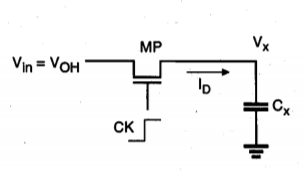
Fig 2: Equivalent circuit for the logic " 1 " transfer event.
The pass transistor MP operating in the saturation region starts to charge up the capacitor Cx, thus,

Note that the threshold voltage of the pass transistor is actually subject to substrate bias effect and therefore, depends on the voltage level V. To simplify our analysis, we will neglect the substrate bias effect at this point. Integrating above equation


This equation can be solved for Vx(t), as follows.
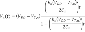
The variation of the node voltage V according to above equation is plotted as a function of time in Figure shown below. The voltage rises from its initial value of 0 V and approaches a limit value for large t, but it cannot exceed its limit value of Vmax = (VDD - VT,). The pass transistor will turn off when Vx=Vmax, since at this point, its gate-to-source voltage will be equal to its threshold voltage. Therefore, the voltage at node X can never attain the full power supply voltage level of VDD during the logic "1" transfer. The actual value of the maximum possible voltage Vmax at node X can be found by taking into account the substrate bias effect for MP.


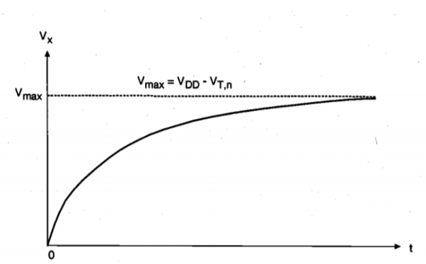
Fig 3 Variation of Vx as a function of time during logic "I" transfer
Thus, the voltage Vx which is obtained at node X following a logic " 1" transfer can be considerably lower than VDD. Also note that the rise time of the voltage V will be underestimated if the zero-bias threshold voltage V. In that case, the actual charge-up time will be longer than predicted by figure above, because the drain current of the nMOS transistor is decreased due to the substrate bias effect.
The fact that the node voltage Vx has an upper limit of Vmax = (VDD - VT,) has a significant implication for circuit design. As an example, consider the following case in which a logic "1" at the input node (Vin = VDD) shown is being transferred through a chain of cascaded pass transistors as shown below. The first pass transistor Ml operates in saturation with VDS1> VGSI – VT, nl. Therefore, the voltage at node 1 cannot exceed the limit value Vmax, = VDD – VT, n1. Now, assuming that the pass transistors in this circuit are identical, the second pass transistor M2 operates at the saturation boundary. As a result, the voltage at node 2 will be equal to Vmax2 = (VDD - VTn2). It can easily be seen that with VT, nl = VT, n2 = VT, n3 ... , the node voltage at the end of the pass transistor chain will become one threshold voltage lower than VDD, regardless of the number of pass transistors in the chain. It can be observed that the steady-state internal node voltages in this circuit are always one threshold voltage below VDD, regardless of the initial voltages.

Fig 4 Node voltages in a pass-transistor chain during the logic " 1 " transfer
Now consider a different case in which the output of each pass transistor drives the gate of another pass transistor, as depicted in Figure below.

Fig 5 Node voltages during the logic " 1 " transfer, when each pass transistor is driving another pass transistor.
Here, the output of the first pass transistor Ml can reach the limit Vm = (VDD – VT, nl). This voltage drives the gate of the second pass transistor, which also operates in the saturation region. Its gate-to-source voltage cannot exceed VT,n2, hence, the upper limit for V2 is found as Vmax2 = VDD – VT,n1 – VT,n2. It can be seen that in this case, each stage causes a significant loss of voltage level. The amount of voltage drop at each stage can be approximated more realistically by taking into account the corresponding substrate bias effect, which is different in all stages.


The preceding analysis helped us to examine important characteristics of the logic 1 " transfer event. Next, we will examine the charge-down event, which is also called a logic "0" transfer.
Logic "0" Transfer
Assume that the soft-node voltage V is equal to a logic " 1 " level initially, i.e., Vx(t = 0) = Vm = (VDD- VTn). A logic "" level is applied to the input terminal, which corresponds to Vin = 0 V. Now, the clock signal at the gate of the pass transistor goes from 0 to VDD at t = 0. The pass transistor MP starts to conduct as soon as the clock signal becomes active, and the direction of drain current flow through MP will be opposite to that during the charge-up (logic " 1 " transfer) event. This means that the intermediate node X will now correspond to the drain terminal of MP and that the input node will correspond to its source terminal. With VGS = VDD and VDS = Vmax, it can be seen that the pass transistor operates in the linear region throughout this cycle, since VDS < VGS - VTn.
The circuit to be analysed for the logic "0" transfer event can be simplified into an equivalent circuit as shown in Figure below. As in the logic " 1 " transfer case, the depletion load nMOS inverter does not affect this event.
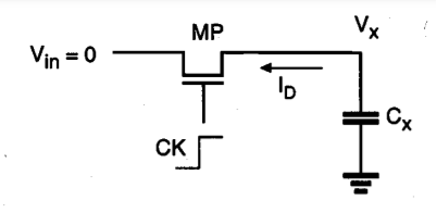
Fig 6 Equivalent circuit for the logic "0" transfer event.
The pass transistor MP operating in the linear region discharges the parasitic capacitor Cx, as follows:


Note that the source voltage of the nMOS pass transistor is equal to 0 V during this event; hence, there is no substrate bias effect for MP (VTn = VT0, n). But the initial condition: Vx (t = 0) = (VDD - VTn) contains the threshold voltage with substrate bias effect, because the voltage V is set during the preceding logic "1" transfer event. To simplify the expressions, we will use VT, in the following. Integrating both sides of above equation yields


Finally, the fall-time expression for the node voltage V can be obtained as

The variation of the node voltage Vx according to above equation is plotted as a function of time in Figure below. It is seen that the voltage drops from its logic-high level of Vmax to 0 V. Hence, unlike the charge-up case, the applied input voltage level (logic 0) can be transferred to the soft node without any modification during this event.
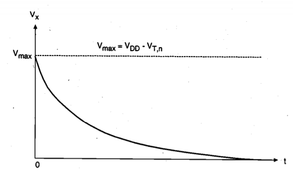
Fig 7 Variation of Vx as a function of time during logic "O" transfer.
The fall time ( fall) for the soft-node voltage V. Can be calculated from above equation as follows. First, define the two time points t90% and t10% as the times at which the node voltage is equal to 0.9 Vmax and 0.1 Vmax, respectively. These two time points can easily be found by using above equation.


The fall time of the soft-node voltage Vx is by definition the difference between t10% and t90%, which is found as


Until this point, we have examined the transient charge-up and charge-down events which are responsible for logic "1" transfer and logic "0" transfer during the active clock phase, i.e., when CK = 1. Now we will turn our attention to the storage of logic levels at the soft node X during the inactive clock cycle, i.e., when CK = 0.
Charge Storage and Charge Leakage
As already discussed qualitatively in the preceding section, the preservation of a correct logic level at the soft node during the inactive clock phase depends on preserving a sufficient amount of charge in Cx, despite the leakage currents. To analyze the events during the inactive clock phase in more detail, consider the scenario shown in Fig. Below. We will assume that a logic-high voltage level has been transferred to the soft node during the active clock phase and that now both the input voltage Vn and the clock are; equal to 0 V. The charge stored in Cx will gradually leak away, primarily due to the leakage currents associated with the pass transistor. The gate current of the inverter driver transistor is negligible for all practical purposes.
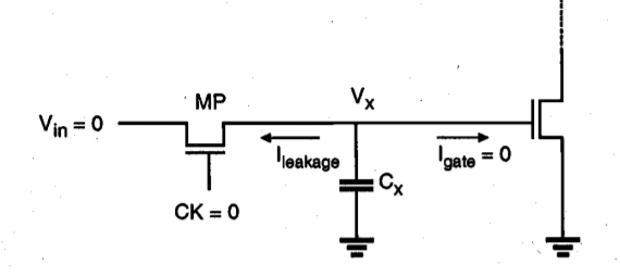
Fig 8 Charge leakage from the soft node.
Figure above shows a simplified cross-section of the nMOS pass transistor, together with the lumped node capacitance Cx. We see that the leakage current responsible for draining the soft-node capacitance over time has two main components, namely, the subthreshold channel current and the reverse conduction current of the drain-substrate junction.
Ileakage = Isubthreshold(MP) + Ireverse(MP)
Note that a certain portion of the total soft-node capacitance Cx, is due to the reverse biased drain-substrate junction, which is also a function of the soft-node voltage V. Other components of Cx, which are primarily due to oxide-related parasitics, can be considered constants. In our analysis, these constant capacitance components will be represented by Cin. Thus, we have to express the total charge stored in the soft node as the sum of two main components, as follows.


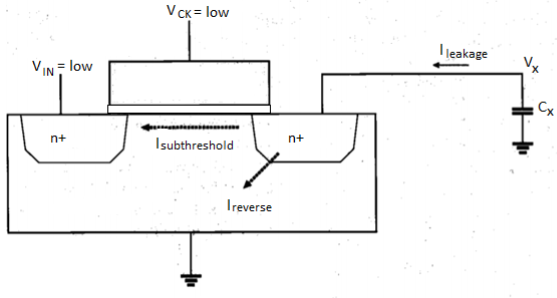
Fig 9 Simplified cross-section of the nMOS pass transistor, showing the leakage current components responsible for draining the soft-node capacitance Cx.
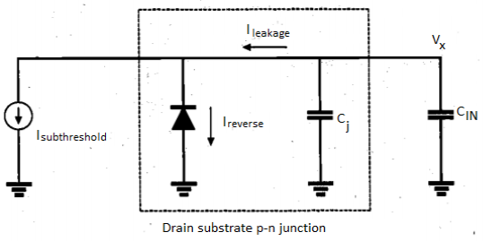
Fig 10 Equivalent circuit used for analysing the charge leakage process
The total leakage current can be expressed as the time derivative of the total soft-node charge Q.


Also note that the subthreshold current in deep-submicron transistors can significantly exceed the reverse conduction current, especially for VDS = VDD. In long-channel transistors, the magnitude of the subthreshold current can be comparable to that of the reverse leakage current. The reverse conduction current in turn has two main components, the constant reverse saturation current I, and the generation current Igen which originates in the depletion region and is a function of the applied bias voltage V. To estimate the actual charge leakage time from the soft node, we have to solve the differential equation, taking into account the voltage-dependent capacitance components and the nonlinear leakage currents. For a quick estimate of the worst case leakage behavior, on the other hand, the problem can be further simplified.
Assume that the minimum combined soft-node capacitance is given as

Where Cdbmin represents the minimum junction capacitance, obtained under the bias condition Vx = Vmax. Now we define the worst-case holding time (thold) as the shortest time required for the soft-node voltage to drop from its initial logic-high
Value to the logic threshold voltage due to leakage. Once the soft-node voltage reaches the logic threshold, the logic stage being driven by this node will lose its previously held state.


Key takeaway
Pass transistor logic attempts to reduce the number of transistors required to implement logic by allowing the primary inputs to drive gate terminals as well as source/drain terminals. This is in contrast to logic families that we have studied so far that only allow primary inputs to drive the gate terminals of MOSFETS.
Example
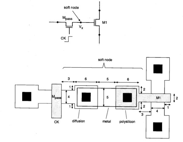
Consider the soft-node structure shown below, which consists of the drain (or source, depending on current direction) terminal of the pass transistor, connected to the polysilicon gate of an nMOS driver transistor via a metal interconnect.
Sol:
We will assume that the power supply voltage used in this circuit is VDD = V, and that the soft node has initially been charged up to its maximum voltage, V. In order to estimate the worst-case holding time, the total soft-node capacitance must be calculated first. The simplified mask layout of the structure is shown in the following. All dimensions are given in micrometers. The critical material parameters to be used in this example are listed below.


First, we calculate the oxide-related (constant) parasitic capacitance components associated with the soft node.


Now, we have to calculate the parasitic junction capacitance associated with the drain substrate pn-junction of the pass transistor. Using the zero-bias unit capacitance values given here, we obtain


The minimum value of the drain junction capacitance is achieved when the junction is biased (in reverse) with its maximum possible voltage, Vmx. In order to calculate the minimum capacitance value, we first find Vmax


Now, the minimum value of the drain junction capacitance can be calculated.

The minimum value of the total soft-node capacitance is found by

The amount of the critical charge drops in the soft node, which will eventually cause a change of logic state, is


Assuming that the logic threshold voltage of the next gate is (VDD/2). In this example, the maximum leakage current responsible for charge depletion is given from the MOS characteristics

Finally, we calculate the worst-case (minimum) hold time for the soft node using the expression

Key takeaway
It is interesting to note that even with a very small soft-node capacitance of 8.55 fF, the worst-case hold time for this structure is relatively long, especially compared with the signal propagation delays encountered in nMOS or CMOS logic gates. This example proves the feasibility of the dynamic charge storage concept and shows that a logic state can be safely preserved in a soft node for long time periods.
The digital circuit design techniques, which take advantage of this simple yet effective principle. In the following, we will investigate different examples of synchronous dynamic circuits implemented using depletion-load nMOS, enhancement-load nMOS, and CMOS building blocks.
Dynamic Pass Transistor Circuits
Consider the generalized view of a multi-stage synchronous circuit shown in Figure below. The circuit consists of cascaded combinational logic stages, which are interconnected through nMOS pass transistors. All inputs of each combinational logic block are driven by a single clock signal. Individual input capacitances are not shown in this figure for simplicity, but the operation of the circuit obviously depends on temporary charge storage in the parasitic input capacitances.
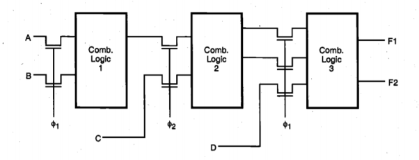
Fig. 11 Multi-stage pass transistor logic driven by two nonoverlapping clocks.
To drive the pass transistors in this system, two nonoverlapping clock signals, ɸ1and ɸ2, are used. The nonoverlapping property of the two clock signals guarantees that at any given time point, only one of the two clock signals can be active, as illustrated in Figure below. When clock ɸ1, is active, the input levels of Stage 1 (and also of Stage 3) are applied through the pass transistors, while the input capacitances of Stage 2 retain their previously set logic levels. During the next phase, when clock ɸ2 is active, the input levels of Stage 2 will be applied through the pass transistors, while the input capacitances of Stage 1 and Stage 3 retain their logic levels. This allows us to incorporate the simple dynamic memory function at each stage input, and at the same time, to facilitate synchronous operation by controlling the signal flow in the circuit using the two periodic clock signals. This signal timing scheme is also called two-phase clocking and is one of the most widely used timing strategies.
By introducing the two-phase clocking scheme, we have not made any specific assumptions about the internal structure of the combinational logic stages. It will be seen that depletion-load nMOS, enhancement-load nMOS, or CMOS logic circuits can be used for implementing the combinational logic. Figure below shows a depletion-load dynamic shift register circuit, in which the input data are inverted once and transferred, or shifted into the next stage during each clock phase.
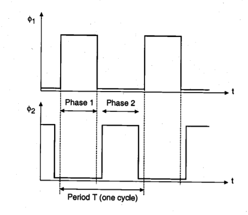
Fig 12 Nonoverlapping clock signals used for two-phase synchronous operation.
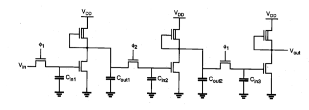
Fig 13 Three stages of a depletion-load nMOS dynamic shift register circuit driven with two-phase clocking.
The operation of the shift register circuit is as follows. During the active phase of ɸ1 the input voltage level Vin is transferred into the input capacitance Cin. Thus, the valid output voltage level of the first stage is determined as the inverse of the current input during this cycle. When ɸ2 becomes active during the next phase, the output voltage level of the first stage is transferred into the second stage input capacitance Cin2, and the valid output voltage level of the second stage is determined. During the active ɸ2 phase, the first-stage input capacitance continues to retain its previous level via charge storage. When ɸ1 becomes active again, the original data bit written into the register during the previous cycle is transferred into the third stage, and the first stage can now accept the next data bit.
In this circuit, the maximum clock frequency is determined by the signal propagation delay through one inverter stage. One half-period of the clock signal must be long enough to allow the input capacitance Cin, to charge up or down, and the logic level to propagate to the output by charging Cout. Also notice that the logic-high input level of each inverter stage in this circuit is one threshold voltage lower than the power supply voltage level. The same operation principle used in the simple shift register circuit can easily be extended to synchronous complex logic. Figures below show a two-stage circuit example implemented using depletion-load nMOS complex logic gates.
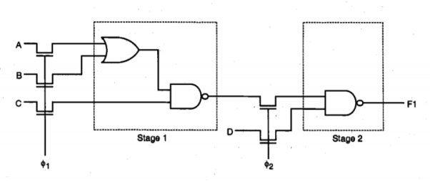
Fig 14 A two-stage synchronous complex logic circuit example
In a complex logic circuit such as the one shown in Figure below, we see that the signal propagation delay of each stage may be different. Thus, in order to guarantee that correct logic levels are propagated during each active clock cycle, the half-period length of the clock signal must be longer than the largest single-stage signal propagation delay found in the circuit.
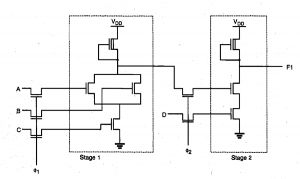
Fig 15 Depletion-load nMOS implementation of synchronous complex logic.
Now consider a different implementation of the simple shift register circuit, using enhancement-load nMQS inverters. One important difference is that, instead of biasing the load transistors with a constant gate voltage, we apply the clock signal to the gate of the load transistor as well. It can be shown that the power dissipation and the silicon area can be reduced significantly by using this dynamic (clocked) load approach. Two variants of the dynamic enhancement-load shift register will be examined in the following, both of which are driven by two non-overlapping clock signals. Figure below shows the first implementation, where in each stage the input pass transistor and the load transistor are driven by opposite clock phases, ɸ1 and ɸ2.
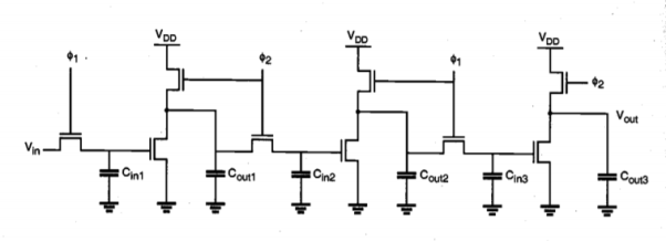
Fig 16 Enhancement-load dynamic shift register (ratioed logic)
When ɸ1 is active, the input voltage level Vi. Is transferred into the first-stage input capacitance CinI through the pass transistor. In this phase, the enhancement-type nMOS load transistor of the first-stage inverter is not active yet. During the next phase, the load transistor is turned on. Since the input logic level is still being preserved in Cin1, the output of the first inverter stage attains its valid logic level. At the same time, the input pass transistor of the second stage is also turned on, which allows this newly determined output level to be transferred into the input capacitance Cin2 of the second stage.
When clock ɸ1 becomes active again, the valid output level across Cout2 is determined, and transferred into Cin3. Also, a new input level can be accepted (pipelined) into Cin, during this phase. In this circuit, the valid low-output voltage level VOL of each stage is strictly determined by the driver-to-load ratio, since the output pass transistor (input pass transistor of next stage) turns on in phase with the load transistor. Therefore, this circuit arrangement is also called ratioed dynamic logic. The basic operation principle can obviously be extended to arbitrary complex logic, as shown in Fig. Below. Since the power supply current flows only when the load devices are activated by the clock signal, the overall power consumption of dynamic enhancement-load logic is generally lower than for depletion-load nMOS logic.

Fig 17 General circuit structure of ratioed synchronous dynamic logic.

Fig 18 Enhancement-load dynamic shift register (ratio less logic).
When ɸ1 is active, the input voltage level Vin is transferred into the first-stage input capacitance Cin,1 through the pass transistor. Note that at the same time, the enhancement type nMOS load transistor of the first-stage inverter is active. Therefore, the output of the first inverter stage attains its valid logic level. During the next phase (active ɸ2), the input pass transistor of the next stage is turned on, and the logic level is transferred onto the next stage. Here, we have to consider two cases, as follows.
If the output level across Cout,1 is logic-high at the end of the active ɸI phase, this voltage level is transferred to Cin2 via charge sharing over the pass transistor during the active ɸ2 phase. Note that the logic-high level at the output node is subject to threshold voltage drop, i.e., it is one threshold voltage lower than the power supply voltage. To correctly transfer a logic-high level after charge sharing, the ratio of the capacitors (Cout/ Cin) must be made large enough during circuit design.
If, on the other hand, the output level of the first stage is logic-low at the end of the active ɸ phase, then the output capacitor Cout, l will be completely drained to a voltage of VOL = 0 V when 1 turns off. This can be achieved because a logic-high level is being stored in the input capacitance Cin, l in this case, which forces the driver transistor to remain in conduction. Obviously, the logic-low level of VOL = 0 V is also transferred into the next stage via the pass transistor during the active ɸ2 phase.
When clock ɸ1, becomes active again, the valid output level across Cout2 is determined and transferred into Cin3. Also, a new input level can be accepted into Cin1, during this phase. Since the valid logic-low level of VOL = 0 V can be achieved regardless of the driver-to-load ratio, this circuit arrangement is called ratio less dynamic logic. The basic operation principle can be extended to arbitrary complex logic, as shown in Figure.

Fig 19 General circuit structure of ratio less synchronous dynamic logic.
CMOS Transmission Gate Logic
The basic two-phase synchronous logic circuit principle, in which individual logic blocks are cascaded via clock-controlled switches, can easily be adopted to CMOS structures as well. Here, static CMOS gates are used for implementing the logic blocks, and CMOS transmission gates are used for transferring the output levels of one stage to the inputs of the next stage (Figure below). Notice that each transmission gate is actually controlled by the clock signal and its complement. As a result, two-phase clocking in CMOS transmission gate logic requires that a total of four clock signals are generated and routed throughout the circuit.
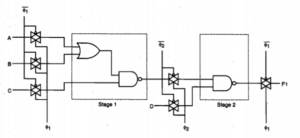
Fig 20 Typical example of dynamic CMOS transmission gate logic.
As in the nMOS-based dynamic circuit structures, the operation of CMOS dynamic logic relies on charge storage in the parasitic input capacitances during the inactive clock cycles. To illustrate the basic operation principles, the fundamental building block of a dynamic CMOS transmission gate shift register is shown in Figure below. It consists of a CMOS inverter, which is driven by a CMOS transmission gate. During the active clock phase (CK =1), the input voltage Vin is transferred onto the parasitic input capacitance C, via the transmission gate. Note that the low on-resistance of the CMOS transmission gate usually results in a smaller transfer time compared to those for nMOS-only switches. Also, there is no threshold voltage drop across the CMOS transmission gate. When the clock signal becomes inactive, the CMOS transmission gate turns off and the voltage level across Cx, can be preserved until the next cycle.

Fig 21 Basic building block of a CMOS transmission gate dynamic shift register
Figure below shows a single-phase CMOS shift register, which is built by cascading identical units as in Figure above and by driving each stage alternately with the clock signal and its complement.

Figure 22 Single-phase CMOS transmission gate dynamic shift register.
Ideally, the transmission gates of the odd-numbered stages would conduct during the active clock phase (when CK = 1), while the transmission gates of the even-numbered stages are off, so that the cascaded inverter stages in the chain are alternately isolated. This would ensure that inputs are permitted in alternating half cycles. In practice, however, the clock signal and its complement do not constitute a truly nonoverlapping signal pair, since the clock voltage waveform has finite rise and fall times. Also, the clock. Skew between CK and CK’ may be unavoidable because one of the signals is generated by inverting the other. Therefore, true two-phase clocking with two nonoverlapping clock signals (ɸ1 and ɸ2) and their complements is usually preferred over single-phase clocking in dynamic CMOS transmission gate logic.
A dynamic CMOS circuit technique which allows us to significantly reduce the number of transistors used to implement any logic function. The circuit operation is based on first precharging the output node capacitance and subsequently, evaluating the output level according to the applied inputs. Both of these operations are scheduled by a single clock signal, which drives one nMOS and one pMOS transistor in each dynamic stage.
A dynamic CMOS logic gate which implements the function

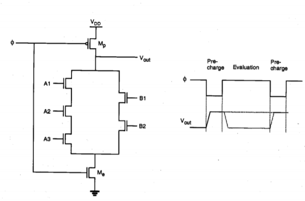
Fig 23 Dynamic CMOS logic gate implementing a complex Boolean function.
When the clock signal is low (precharge phase), the pMOS precharge transistor MP is conducting, while the complementary nMOS transistor Me is off. The parasitic output capacitance of the circuit is charged up through the conducting pMOS transistor to a logic-high level of Vout = VDD. The input voltages are also applied during this phase, but they have no influence yet upon the output level since Me is turned off.
When the clock signal becomes high (evaluate phase), the precharge transistor Mp turns off and Me turns on. The output node voltage may now remain at the logic- high level or drop to a logic low, depending on the input voltage levels. If the input signals create a conducting path between the output node and the ground, the output capacitance will discharge toward VOL = 0 V. The final discharged output level depends on the time span of the evaluation phase. Otherwise, Vout, remains at VDD.
The operation of the single-stage dynamic CMOS logic gate is quite straightforward. For practical multi-stage applications, however, the dynamic CMOS gate presents a significant problem. To examine this fundamental limitation, consider the two-stage cascaded structure shown in Figure below. Here, the output of the first dynamic CMOS stage drives one of the inputs of the second dynamic CMOS stage, which is assumed to be a two input NAND gate for simplicity.
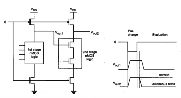
Fig 24 Illustration of the cascading problem in dynamic CMOS logic
During the precharge phase, both output voltages Vout1 and Vout2 are pulled up by the respective pMOS precharge devices. Also, the external inputs are applied during this phase. The input variables of the first stage are assumed to be such that the output Vout1 will drop to logic "0" during the evaluation phase. On the other hand, the external input of the second-stage NAND2 gate is assumed to be a logic " 1," as shown in Figure above. When the evaluation phase begins, both output voltages Vout, l and Vout2 are logic-high. The output of the first stage (Vocal) eventually drops to its correct logic level after a certain time delay. However, since the evaluation in the second stage is done concurrently, starting with the high value of Vout, l at the beginning of the evaluation phase, the output voltage Vout2 at the end of the evaluation phase will be erroneously low. Although the first stage output subsequently assumes its correct output value once the stored charge is drained, the correction of the second-stage output is not possible. This example illustrates that dynamic CMOS logic stages driven by the same clock signal cannot be cascaded directly. This severe limitation seems to undermine all the other advantages of dynamic CMOS logic, such as low power dissipation, large noise margins, and low transistor count. Alternative clocking schemes and circuit structures must be developed to overcome this problem.
Key takeaway
A dynamic CMOS circuit technique which allows us to significantly reduce the number of transistors used to implement any logic function. The circuit operation is based on first precharging the output node capacitance and subsequently, evaluating the output level according to the applied inputs. Both of these operations are scheduled by a single clock signal, which drives one nMOS and one pMOS transistor in each dynamic stage.
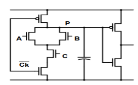
Fig 25 CMOS Domino logic
Another way to eliminate the problem with cascading logic stages is to use a static inverter after the CMOS dynamic gate. Recall that the cascaded dynamic CMOS stage causes problems because the output is pre-charged to Vdd. If the final value is meant to be zero, the next stage nMOS to which the output is connected erroneously sees a one till the pre-charged output is brought down to zero. During this time, it ends up discharging its own pre-charged output, which it was not supposed to do. If an inverter is added, the output is held ‘low’ before logic evaluation. If the final output is zero, there is no problem anyway. If the final output is supposed be one, the next stage is erroneously held at zero for some time. However, this does not result in a false evaluation by the next stage. The only effect it can have is that the next stage starts its evaluation a little later. However, the addition of an inverter means that the logic is non-inverting. Therefore, it cannot be used to implement any arbitrary logic function.
Key takeaway
If the final value is meant to be zero, the next stage nMOS to which the output is connected erroneously sees a one till the pre-charged output is brought down to zero. During this time, it ends up discharging its own pre-charged output, which it was not supposed to do.
Semiconductor memory arrays capable of storing large quantities of digital information are essential to all digital systems. The amount of memory required in a particular system depends on the type of application, but, in general, the number of transistors utilized for the information (data) storage function is much larger than the number of transistors used in logic operations and for other purposes. The ever-increasing demand for larger data storage capacity has driven the fabrication technology and memory development towards more compact design rules and, consequently, toward higher data storage densities. Thus, the maximum realizable data storage capacity of single-chip semiconductor memory arrays approximately doubles every two years. On-chip memory arrays have become widely used subsystems in many VLSI circuits, and commercially available single-chip read/write memory capacity has reached 64 megabits. This trend toward higher memory density and larger storage capacity will continue to push the leading edge of digital system design.
The area efficiency of the memory array, i.e., the number of stored data bits per unit area, is one of the key design criteria that determine the overall storage capacity and, hence, the memory cost per bit. Another important issue is the memory access time, i.e., the time required to store and/or retrieve a particular data bit in the memory array. The access time determines the memory speed, which is an important performance criterion of the memory array. Finally, the static and dynamic power consumption of the memory array is a significant factor to be considered in the design, because of the increasing importance of low-power applications. In the following, we will investigate different types of MOS memory arrays and discuss in detail the issues of area, speed, and power consumption for each circuit type.
Memory circuits are generally classified according to the type of data storage and the type of data access. Read-Only Memory (ROM) circuits allow, as the name implies, only the retrieval of previously stored data and do not permit modifications of the stored information contents during normal operation. ROMs are non-volatile memories, i.e., the data storage function is not lost even when the power supply voltage is off. Depending on the type of data storage (data write) method, ROMs are classified as mask-programmed ROMs, Programmable ROMs (PROM), Erasable PROMs (EPROM), and Electrically Erasable PROMs (EEPROM).
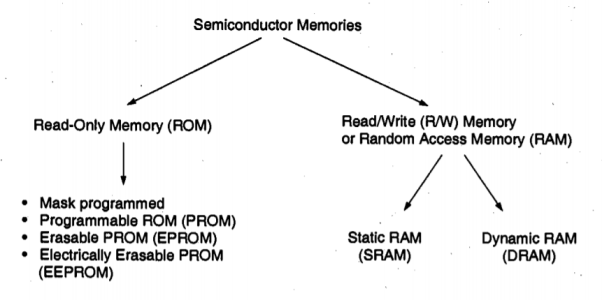
Fig 26 Overview of semiconductor memory types.
Dynamic Read-Write Memory (DRAM)
In the static CMOS read-write memory data is stored in six-transistor cells. Such a memory is fast and consumed small amount of static power. The only problem is that a SRAM cell occupies a significant amount of silicon space. This problem is addressed in the dynamic read-write memory (DRAM). In a dynamic RAM binary data is stored as charge in a capacitor. The memory cell consists of a storage capacitor and an access transistor as shown in Figure
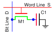
Fig 27 A one-transistor DRAM memory cell
Data stored as charge in a capacitor can be retained only for a limited time due to the leakage current which eventually removes or modifies the charge. Therefore, all dynamic memory cells require a periodic refreshing of the stored data before unwanted stored charge modifications occur. Typical storage capacitance has a value of 20 to 50 fF. Assuming that the voltage on the fully charged storage capacitor is V = 2.5V, and that the leakage current is I = 40pA
The DRAM cell occupies much smaller silicon area than the SRAM cell. The size of a DRAM cell is in the order of 8F2, where F is the smallest feature size in a given technology. For F = 0.2μm the size is 0.32μm2
• No static power is dissipated for storing charge in a capacitance. The storage capacitance CS, which is connected between the drain of the access transistor (the storage node) and the ground, is formed as a trench or stacked Capacitor. The stacked capacitor is created between a second polysilicon layer and a metal plate covering the whole array area. The plate is effectively connected to the ground terminal. To consider read/write operations we have to take into account a significant parasitic capacitance CC associated with each column, as shown in Figure

Fig 28 A single SRAM cells with a column capacitance shown
Typically, before any operation is performed each column capacitance b is precharged high. The cell is selected for a read/write operation by asserting its word line high (S = 1). This connects the storage capacitance to the bit line. The write operation is performed by applying either high or low voltage to the bit line thus charging (write ‘1’) or discharging (write ‘0’) the storage capacitance through the access transistor. During read operation there is a flow of charges between the storage capacitance C1 and the column capacitance, CC.
As a result, the column voltage either increases (read ‘1’) or decreases (read ‘0’) slightly. This difference can then be amplified by the sense amplifier. Note that the read operation destroys the charge stored on the storage capacitance C1 (“destructive readout”). Therefore, the data must be restored (refreshed) each time the read operation is performed.
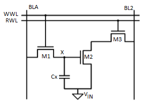
Fig 29 Three Transistor Dynamic RAM
The write operation performed is shown for three transistor Dynamic RAM (Figure 1.2) as the appropriate data value is written on BL1 and asserting the write-wordline (WWL). The data is retained as charge on capacitance Cs once WWL is lowered. When reading the cell, the readwordline (RWL) is raised. The storage transistor M2 is either on or off depending upon the stored value. The bitline BL2 is precharged to VDD before performing read operation. The series connection of M2 and M3 pulls BL2 low when a “1” is stored. BL2 remains high in the opposite case. The cell is inverting; that is, the inverse value of the stored signal is sensed on the bitline.
DRAM Timing:
DRAM module is asynchronous, Timing depends on how long it takes to respond to each operation.
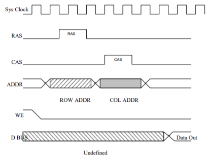
Fig 30 Timing Diagram
Key takeaway
DRAM cannot be read as fast (or as easy) as SRAM.
Static Random Access Memory (SRAM)
The typical SRAM design is shown in figure the memory array contains the memory cells which are readable and writable. The Row decoder selects from 1 out of n = 2k rows, while the column decoder selects l = 2i out of m = 2j columns. The addresses are not multiplexed as it in the DRAM. Sense amplifier detects small voltage variations on the memory complimentary bitline which reduces the reading time. The conditioning circuit is used to pre-charge the bitlines.
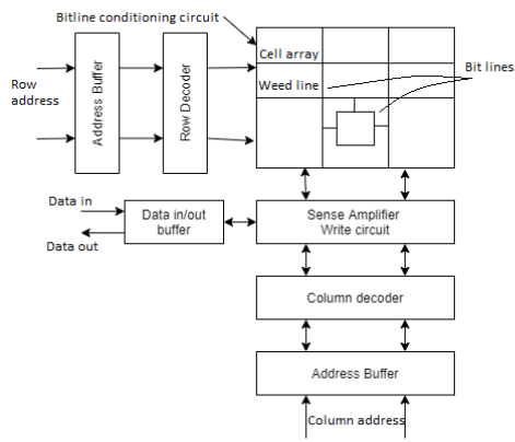
Fig 31 SRAM Architecture
In a read operation, the bitlines are precharged to some reference voltage usually close to the supply voltage. When word line turns high, the access transistor connected to the node storing „0‟ starts discharging the bitline while the complementary bitline remains in its precharged state, resulting in a differential voltage between the bitline pair. Since the SRAM has an optimized area results in a small cell current and slow bitline discharge rate. In order to speed up the RAM access, sense amplifiers are used which amplify the small bitline signal and eventually drive it to the external world.
The word “static” means that the memory retains its contents as long as the power is turned on. Random access means that locations in the memory can be written to or read from in any order, regardless of the memory location that was last accessed. Each bit in an SRAM is stored on four transistors that form two cross-coupled inverters. This storage cell has two stable states which are used to denote „0‟ and „1‟.
The access transistors are used to access the stored bits in the SRAM during read or write mode. It thus typically takes six MOSFETs to store one memory bit. Access to the cell is enabled by the word line WL which controls the two access transistors N1 and N2 which, in turn, control whether the cell should be connected to the bitlines BL and /BL. They are used to transfer data for both read and write operations.
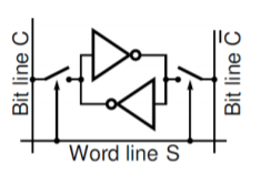
Fig 32 A logic diagram of a CMOS static memory cell
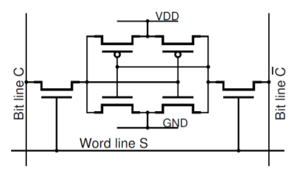
Fig 33 A schematic of a CMOS static memory cell
Principles of operations
In order to consider operation of the static read/write memory we have to take into account: Relatively large parasitic column capacitances, CC and Cc
Column pull-up pMOS transistors, as shown in Figure
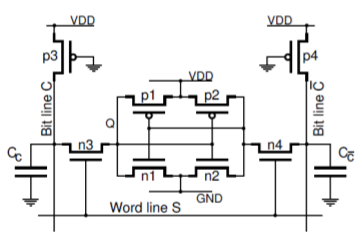
Fig 34 A CMOS static memory cell with column pull-up transistors and parasitic column capacitances
When none of the word lines is selected, that is, all S signals are ‘0’, the pass transistors n3, n4 are turned off and the data is retained in all memory cells. The column capacitances are charged by the drain currents of the pull-up pMOS transistors, p3, p4. The column voltages VC and V c¯ both reach the level just below VDD − VT p, say 3.5V for VDD = 5V and the threshold voltage VT p = 1V.
For the read or write operations we select the cell asserting the word line signal S= ‘1’. For the write operation we apply a low voltage to one of the bit line, holding the other one high. To write ‘0’ in the cell, the column voltage VC is forced to low (C = 0). This low voltage acts through a related pass transistor (n3) on the gates of the corresponding inverter (n2, p2) so that its input goes high. This sets the signal at the other inverter Q = 0. Similarly, to write ‘1’ in the cell, the opposite column voltage VC¯ is forced to low (C¯ = 0) which sets the signal Q = 1.
During the read ‘1’ operation, when the stored bit is Q = 1, transistors n3, p1 and n4, n2 are turned on. This maintains the column voltage VC at its steady state high level (say 3.5V) while the opposite column voltage VC¯ is being pulled down discharging the column capacitance CC¯ through transistors n4, n2 so that VC > VC¯. Similarly, during the read ‘0’ operation we have VC < VC¯. The difference between the column voltages is small, say 0.5V, and must be detected by the sense amplifiers from data-read circuitry.
SRAM Read Circuitry
The structure of the read circuitry is shown in Figure
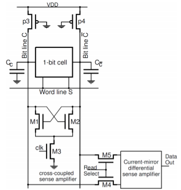
Fig 35 The structure of the write circuitry associated with one column of the memory cells. During the read operation the voltage level on one of the bit lines drops slightly after the pass transistors in the memory cell are turned on.
The read circuitry consists of two-level sense amplifiers:
• One simple cross-coupled sense amplifier per column of memory cells,
• One current-mirror differential sense amplifier per the memory chip.
The cross-coupled sense amplifier works as a latch. Assume that the voltage on the bit line C start to drop slightly when the memory access pass transistors are activated by the word line signal S, and that the clk signal is high so that the transistor M3 is turned on. Now, higher voltage on the gate of M1 transistor than on the gate of M2 starts the latching operation which pulls the VC voltage further down switching the transistor M2 off.
As a result, the parasitic capacitance, CC is discharged through M1 and M3. In this way a small difference between column voltages is amplified. The amplified (discriminated) column voltages are passed through transistors M4 and M5 to the main sense amplifier. The schematic of a typical differential current-mirror sense amplifier is shown in Figure
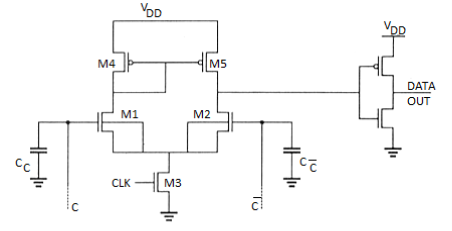
Fig 36 A CMOS differential current-mirror sense amplifier
Key takeaway
Random access memory is a type of computer data storage. It is made of integrated circuits that allow the stored data to be accessed in any order i.e., at random and without the physical movement of storage medium or a physical reading head.
The basic idea of the memory that can only be read and never altered is called Read only memories. There are vast and variety of potential applications for these kind of memories. Programs for processors with fixed applications such as washing machines, calculators and game machines, once developed and debugged, need only reading. Fixing the contents at manufacturing time leads to small and fast implementation. There are different ways to implement the logic of ROM cells, the fact that the contents of a ROM cell are permanently fixed considerably simplifies its design. The cell should be designed so that a „0‟ or „1‟ is presented to the bitline upon activation of its wordline. The different approaches for implementing the ROM cells are Diode ROM, MOS ROM 1 and MOS ROM 2. These are the main approaches for designing a larger density ROMs.
The basic idea of the memory that can only be read and never altered is called Read only memories. There are vast and variety of potential applications for these kind of memories. Programs for processors with fixed applications such as washing machines, calculators and game machines, once developed and debugged, need only reading. Fixing the contents at manufacturing time leads to small and fast implementation. There are different ways to implement the logic of ROM cells, the fact that the contents of a ROM cell are permanently fixed considerably simplifies its design. The cell should be designed so that a „0‟ or „1‟ is presented to the bitline upon activation of its wordline. The different approaches for implementing the ROM cells are Diode ROM, MOS ROM 1 and MOS ROM 2. These are the main approaches for designing a larger density ROMs.
Programmable ROM (PROM):
The technology that offers its users to program the memory one time is called Programmable ROM. It is also called as WRITE ONCE device. This is most often accomplished by introducing fuses (implemented in nichrome, polysilicon, or other conductors) in the memory cell. During the programming phase, some of these fuses are blown by applying a high current, which disables the connected transistor. While PROMs have the advantage of being “customer programmable,” the single write phase makes them unattractive.
For instance, a single error in the programming process or application makes the device unstable. This explains the current preference for devices that can be programmed several times. The Floating-Gate transistor is the device at the heart of the majority of reprogrammable memories. Various attempts have made to create a device with electrically alterable characteristics and enough reliability to support a multitude of write cycles. The floating gate structure is similar to a traditional MOS device, except that an extra polysilicon strip is inserted between the gate and channel.
This strip is not connected to anything and is called a floating gate. The most obvious impact of inserting this extra gate is to double the gate oxide thickness tox, which results in a reduced device transconductance as well as an increased threshold voltage. Though these properties are not desirable but from other point of view this device acts as a normal transistor. The most important property of this device is that the threshold voltage of this device is programmable. By applying a high voltage (above 10V) between the source and the gate-drain terminals creates a high electric field and causes avalanche injection to occur.
Electrons acquire sufficient energy to become “hot” and traverse through the first oxide insulator, so that they get trapped on the floating gate. In reference to the programming mechanism, the floating-gate transistor is often called a floating-gate avalanche- injection MOS. The trapping of electrons on the floating gate effectively drops the voltage on the gate. This process is self-limiting – the negative charge accumulated on the floating gate reduces the electrical field over the oxide so that ultimately it becomes incapable of accelerating any more hot electrons. Virtually all non-volatile memories are currently based on the floating-gate mechanism. Different classes can be identified, based on the erasure mechanism.
Erasable-programmable Read-Only Memory (EPROM):
The erasure mechanism in EPROM is based on the shining ultraviolet light on the cells through a transparent window in the package. The UV radiation renders the oxide to conduct by the direct generation of electron-hole pairs in the material. The erasure process is slow depending on the UV source, it can take from seconds to several minutes. The programming takes several µs/word. Alternatively, there is another problem which exists is the limited endurance - the number of erase/program cycles is limited to a maximum of one thousand mainly as a result of UV erasing procedure. The device thresholds might vary with repeated programming cycles. The on-chip circuitry is designed in such a way that it also controls the value of the thresholds to within a specified range during programming.
The injection of large channel current of 0.5 mA at a control gate voltage of 12.5V causes high power dissipation during programming. On the other hand, EPROM is extremely simple and dense, making it possible to fabricate large memories at a low cost. Therefore, EPROMs were attractive in applications that do not require reprogramming. The major disadvantage of the EPROM is that the erasure procedure has to occur “off system”. This means the memory must be removed from the board and placed in an EPROM programmer for programming.
Electrically Erasable Programmable Read-Only Memory EEPROM)
The disadvantage of the EPROM is solved by using a method to inject or remove charges from a floating-gate namely – tunneling. A modified floating-gate device called FLOTOX (floating-gate tunneling oxide) transistor is used as programmable device that supports an electrical-erasure procedure. It resembles FAMOS (floating-gate avalanche MOS) device, except that a portion of the dielectric separating the floating gate from the channel and drain is reduced in thickness to about 10 nm or less.
The main advantage of this programming approach is that it is reversible; that is, erasing is simply achieved by reversing the voltage applied during the writing process. The electrons injection on floating-gate raises the threshold, while the reverse operation lowers the VT. When a voltage of approximately 10V (equivalent to 109 V/m) is applied over the thin insulator, electrons travel to and from the floating gate through a mechanism called Fowler – Nordheim tunneling.
Key takeaway
ROM can only read data from it under normal working conditions, and can't modify or rewrite data at any time. Its advantage is that the circuit structure is simple, and the data will not be lost after power off; the disadvantage is that it is only suitable for storing those fixed data. The fundamental difference between RAM and ROM is that RAM can write or read memory data at any time under normal operating conditions.
The concept of Flash EEPROMs is a combination of density of EPROM with versatility of EEPROM structures, with cost and functionality ranging from somewhere between two. Most Flash EEPROM devices use the avalanche hot-electron-injection approach to program the device. Erasure is performed using Fowler – Nordheim tunneling, as from EEPROM cells. The main difference is that erasure procedure is performed in bulk for a complete chip or for the subsection of the memory. Erasing complete memory core at once makes it possible to carefully monitor of the device characteristics during erasure.
The monitoring control hardware on the memory chip regularly checks the value of the threshold during erasure, and adjusts the erasure time dynamically. This approach is only practical when erasing large chunks of memory at a time; hence the flash concept. One of the many existing alternatives for Flash EEPROMs memories are ETOX devices. It resembles a FAMOS gate except that a very thin tunneling gate oxide is utilized (10 nm). Different areas of the gate oxide are used for programming and erasure. Programming is performed by applying a high voltage (12V) on the gate and drain terminals for a grounded source, while erasure occurs with the gate rounded and the source at 12V.
The Programming cycle starts with an erase operation. In erase operation, A 0V gate voltage is applied and a 12V supply is given at source. Electrons, if any, are ejected to the source by tunneling. All cells are erased simultaneously. The variations caused in the threshold voltage at the end of erase operation are due to different initial values of cell threshold voltage and variations in oxide thickness. This can be solved in two methods:
1. The array cells are programmed before applying the erase pulse so that the entire threshold starts at approximately same time.
2. An erase pulse of controlled width is applied. Subsequently the whole array is read to ensure that all the cells are erased. If not, another erase pulse is applied followed by the read cycle.
For write (programming) operation, a high voltage is applied to the gate of the selected device. If a „1‟ is applied to the drain at that time, hot electrons are generated and injected onto the floating gate, raising the threshold. Read operation corresponds as the wordline is raised to 5V; it causes a conditional discharge of bitline.
References:
1. D. A. Pucknell and K. Eshraghian, “Basic VLSI Design: Systems and Circuits”, PHI, 3rd Ed.,1994.
2. W.Wolf, Modern VLSI Design: System on Chip, Third Edition, Pearson, 2002.