Unit - 5
Low – Power CMOS Logic Circuits
The increasing prominence of portable systems and the need to limit power consumption (and hence, heat dissipation) in very high density ULSI chips have led to rapid and innovative developments in low-power design during the recent years. The driving forces behind these developments are portable device applications requiring low power dissipation and high throughput, such as notebook computers, portable communication devices and personal digital assistants (PDAs). In most of these cases, the requirements for low power consumption must be met along with equally demanding goals of high chip density and high throughput.
Hence, low-power design of digital integrated circuits has emerged as a very active and rapidly developing field. The limited battery lifetime typically imposes very strict demands on the overall power consumption of the portable system. Although new rechargeable battery types such as Nickel-Metal Hydride (NiMH) are being developed with higher energy capacity than that of the conventional Nickel-Cadmium (NiCd) batteries, revolutionary increase of the energy capacity is not expected in the near future. The energy density (amount of energy stored per unit weight) offered by the new battery technologies (e.g., NiMH) is about 30 Wh/lb, which is still low in view of the expanding applications of portable systems. Therefore, reducing the power dissipation of integrated circuits through design improvement is a major challenge in portable systems design.
The need for low-power design is also becoming a major issue in high-performance digital systems, such as microprocessors, digital signal processors (DSPs) and other applications. The common traits of high-performance chips are the high integration density and the high clock frequency. The power dissipation of the chip, and thus, the temperature, increases with the increasing clock frequency. Since the dissipated heat must be removed effectively to keep the chip temperature at an acceptable level, the cost of packaging, cooling and heat removal becomes a significant factor in these circuits. Several high-performance microprocessor chips designed in the early 1990s (e.g., Intel Pentium, DEC Alpha, and PowerPC) operate at clock frequencies in the range of 100 to 300 MHz, and their typical power consumption is between 20 and 50 W
ULSI reliability is yet another concern which points to the need for low-power design. There is a close correlation between the peak power dissipation of digital circuits and reliability problems such as electromigration and hot-carrier induced device degradation. Also, the thermal stress caused by heat dissipation on chip is a major reliability concern. Consequently, the reduction of power consumption is also crucial for reliability enhancement.
The methodologies which are used to achieve low power consumption in digital systems span a wide range, from device/process level to algorithm level. Device characteristics (e.g., threshold voltage), device geometries and interconnect properties are significant factors in lowering the power consumption. Circuit-level measures such as the proper choice of circuit design styles, reduction of the voltage swing and clocking strategies can be used to reduce power dissipation at the transistor level. Architecture level measures include smart power management of various system blocks, utilization of pipelining and parallelism, and design of bus structures.
Key takeaway
Finally, the power consumed by the system can be reduced by a proper selection of the data processing algorithms, specifically to minimize the number of switching events for a given task. In this chapter, we will primarily concentrate on the circuit- or transistor-level design measures which can be applied to reduce the power dissipation of digital integrated circuits. Various sources of power consumption will be discussed in detail, and design strategies will be introduced to reduce the power dissipation.
The average power consumption in conventional CMOS digital circuits can be expressed as the sum of three main components
(i) the dynamic (switching) power consumption
(ii) the short-circuit power consumption, and
(iii) the leakage power consumption. If the system or chip includes circuits other than conventional CMOS gates that have continuous current paths between the power supply and the ground, a fourth (static) power component should also be considered.
Switching Power Dissipation
This component represents the power dissipated during a switching event, i.e., when the output node voltage of a CMOS logic gate makes a logic transition. In digital CMOS circuits, switching power is dissipated when energy is drawn from the power supply to charge up the output node capacitance. During this charge-up phase, the output node voltage typically makes a full transition from 0 to VDD and one-half of the energy drawn from the power supply is dissipated as heat in the conducting pMOS transistors. Note that no energy is drawn from the power supply during the charge-down phase, yet the energy stored in the output capacitance during charge-up is dissipated as heat in the conducting nMOS transistors, as the output voltage drops from VDD to 0. To illustrate the dynamic power dissipation during switching, consider the circuit example given in Figure below. Here, a two-input NOR gate drives two NAND gates, through interconnection lines. The total capacitive load at the output of the NOR gate consists of (i) the output node capacitance of the gate itself, (ii) the total interconnect capacitance, and (iii) the input capacitances of the driven gates.
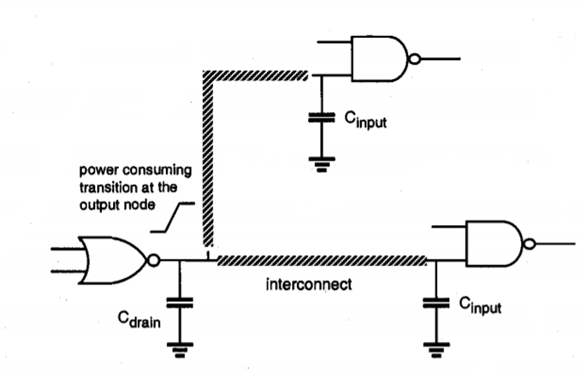
Fig.1 A NOR gate driving two NAND gates through interconnection lines.
The output node capacitance of the gate consists mainly of the junction parasitic capacitances, which are due to the drain diffusion regions of the MOS transistors in the circuit. The amount of diffusion capacitance is approximately a linear function of the junction area. Consequently, the size of the total drain diffusion area dictates the amount of parasitic capacitance at the output node. The interconnect lines between the gates contribute to the second component of the total capacitance. Finally, the input capacitances are mainly due to gate oxide capacitances of the transistors connected to the input terminal. Again, the amount of the gate oxide capacitance is determined primarily by the gate area of each transistor.
Any CMOS logic gate making an output voltage transition can thus be represented by its nMOS network, pMOS network, and the total load capacitance connected to-its output node, as seen in Figure below. The average power dissipation of the CMOS logic gate, driven by a periodic input voltage waveform with ideally zero rise- and fall-times, can be calculated from the energy required to charge up the output node to VDD and charge down the total output load capacitance to ground level.
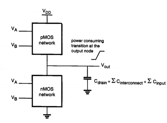
Fig.2 Generic representation of a CMOS logic gate for switching power calculation.

Evaluating these integral yields, the well-known expression for the average dynamic (switching) power consumption in CMOS logic circuits.


Note that the average switching power dissipation of a CMOS gate is essentially independent of all transistor characteristics and transistor sizes as long as a full voltage swing is achieved. Hence, given an input pattern, the switching delay times have no relevance to the amount of power consumption during the switching events as long as the output voltage swing is between 0 and VDD. The analysis of switching power dissipation presented above is based on the assumption that the output node of a CMOS gate undergoes one power-consuming transition (0-to-VDD transition) in each clock cycle. This assumption, however, is not 455 always correct; the node transition rate can be slower than the clock rate, depending on the circuit topology, logic style and the input signal statistics. To better represent this Low-Power behavior, we will introduce aT (node transition factor), which is the effective number of CMOS Logic power-consuming voltage transitions experienced per clock cycle. Then, the average Circuits switching power consumption becomes

The switching power expressions above are derived by taking into account the charge-up and charge-down process of the output node load capacitance Cload' In complex CMOS logic gates, however, most of the internal circuit nodes also make full or partial voltage transitions during switching. Since there is a parasitic capacitance associated with each internal node, these internal transitions contribute to the overall power dissipation of the circuit. In fact, an internal node may undergo several transitions while the output node voltage of the circuit remains unchanged, as illustrated in Figure below. Thus, an underestimation of the overall switching power consumption may result if only output node voltage transitions are considered.
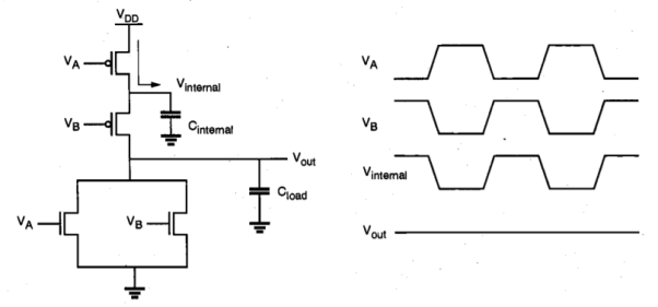
Fig 3 Switching of the. Internal node in a two-input NOR gate results in dynamic power dissipation even if the output node voltage remains unchanged.
In general terms, internal node voltage transitions can be partial, i.e., the node voltage swing may be only Vi which is smaller than the full voltage swing of VDD. Thus, the generalized expression for the average switching power dissipation can be written as

Where C, represents the parasitic capacitance associated with each node in the circuit (including the output node) and αTi, represents the corresponding node transition factor associated with that node.
Short-Circuit Power Dissipation
The switching power dissipation examined above is purely due to the energy required to charge up the parasitic load capacitances in the circuit, and the switching power is independent of the rise and fall times of the input signals. Yet, if a CMOS inverter (or a logic gate) is driven with input voltage waveforms with finite rise and fall times, both the nMOS and the pMOS transistors in the circuit may conduct simultaneously for a short amount of time during switching, forming a direct current path between the power supply and the ground, as shown in Figure below.
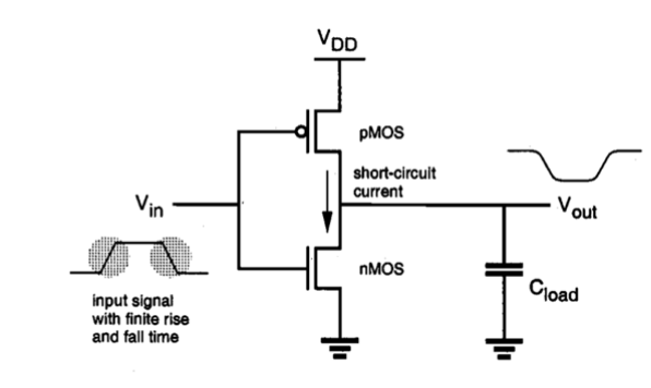
Fig.4 Both nMOS and pMOS transistor may conduct a short circuit current during switching.
CMOS inverter with small capacitive load. The nMOS transistor in the circuit starts conducting when the rising input voltage exceeds the threshold VT,n. The pMOS transistor remains on until the input reaches the voltage level |VDD-VT,p. Thus, there is a time window during which both transistors are turned on. As output capacitance is discharged through the nMOS transistor, the output voltage starts to fall. The drain to source voltage drops of pMOS transistor becomes non-zero which allows the pMOS to conduct. The short circuit current is terminated when the input voltage transition is completed and the pMOS transistor is turned off.
Let us consider asymmetric CMOS inverter with kn=kp=k and VT,n =VT,p =VT and a very small capacitive load. If inverter is driven with input voltage waveform with equal rise and fall time  fall =
  rise=
rise=  . The average short circuit current drawn from the power supply is

Hence, the short-circuit power dissipation becomes

Leakage Power Dissipation
The nMOS and pMOS transistors used in a CMOS logic gate generally have nonzero reverse leakage and subthreshold currents. In a CMOS VLSI chip containing a very large number of transistors, these currents can contribute to the overall power dissipation even when the transistors are not undergoing any switching event. The magnitude of the leakage currents is determined mainly by the processing parameters. Of the two main leakage current components in a MOSFET, the reverse diode leakage occurs when the pn-junction between the drain and the bulk of the transistor is revers-biased. The reverse-biased drain junction then conducts a reverse saturation current which is drawn from the power supply.
Consider a CMOS inverter with a high input voltage, where the nMOS transistor is turned on and the output node voltage is discharged to zero. Although the pMOS transistor is turned off, there will be a reverse potential difference of VDD between its drain and the n-well, causing a diode leakage through the drain junction. The n-well region of the pMOS transistor is also reverse biased with VDD, with respect to the p-type substrate. Therefore, another significant leakage current component exists because of the n-well junction. A similar situation can be observed when the input voltage is zero, and the output voltage is charged up to VDD through the pMOS transistor. Then, the reverse potential difference between the nMOS drain region and the p-type substrate causes a reverse leakage current which is also drawn from the power supply (through the pMOS transistor). The reverse leakage current of a pn-junction is expressed by

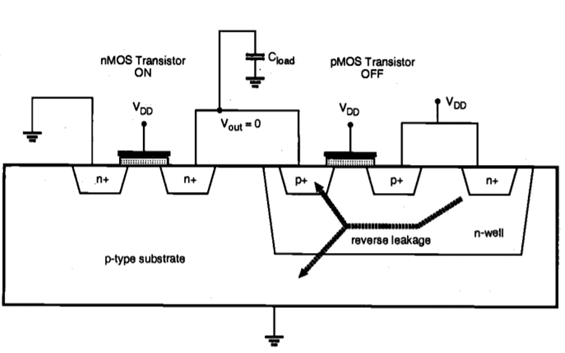
Fig 5 Reverse leakage current paths in a CMOS inverter with high input voltage.
Where Vbias is the reverse bias voltage across the junction, J is the reverse saturation current density and the A is the junction area. The typical reverse saturation current density is 1 - 5 pA/ m2, and it increases quite significantly with temperature. Note that the reverse leakage occurs even during the stand-by operation when no switching takes place. Hence, the power dissipation due to this mechanism can be significant in a large chip containing several million transistors. Another component of leakage currents in CMOS circuits is the subthreshold current, which is due to carrier diffusion between the source and the drain regions of the transistor in weak inversion. The behavior of an MOS transistor in the subthreshold operating region is similar to a bipolar device, and the subthreshold current exhibits an exponential dependence on the gate voltage. The amount of the subthreshold current may become significant when the gate-to-source voltage is smaller than, but very close to, the threshold voltage of the device. In this case, the power dissipation due to subthreshold leakage can become comparable in magnitude to the switching power dissipation of the circuit. The subthreshold leakage current is illustrated in Figure below.
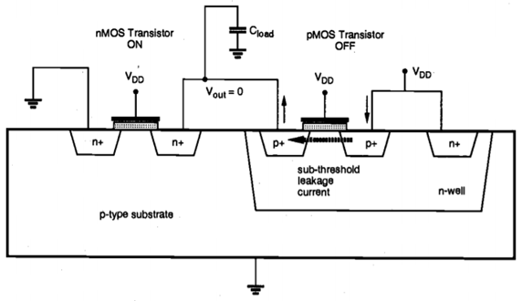
Fig 6 Subthreshold leakage current path in a CMOS inverter with high input voltage.
The subthreshold current expression is given below.

One relatively simple measure to limit the subthreshold current component is to avoid very low threshold voltages, so that the VGs of the nMOS transistor remains safely below VTn when the input is logic zero, and the |VGS| of the pMOS transistor remains safely below IVTI when the input is logic one. In addition to the three major sources of power consumption in CMOS digital integrated circuits discussed in this Section, some chips may also contain circuits which consume static power. One example is the pseudo-nMOS logic circuits which utilize a pMOS transistor as the pull-up device.
Key takeaway
In Switching Power Reduction include
(i) reduction of the power supply voltage VDD,
(ii) reduction of the voltage swing in all nodes,
(iii) reduction of the switching probability (transition factor) and
(iv) reduction of the load capacitance.
Note that the switching power dissipation is also a linear function of the clock frequency, yet simply reducing the frequency would significantly diminish the overall system performance. Thus, the reduction of clock frequency would be a viable option only in cases where the overall throughput of the system can be maintained by other means. The reduction of power supply voltage is one of the most widely practiced measures for low-power design. While such reduction is usually very effective, several important issues must be addressed so that the system performance is not sacrificed.
In particular, we need to consider that reducing the power supply voltage leads to an increase of delay. Also, the input and output signal levels of a low-voltage circuit or module should be made compatible with the peripheral circuitry, in order to maintain correct signal transmission. The reduction of switching activity requires a detailed analysis of signal transition probabilities, and implementation of various circuit-level and system-level measures such as logic optimization, use of gated clock signals and prevention of glitches.
Influence of Voltage Scaling on Power and Delay
Although the reduction of power supply voltage significantly reduces the dynamic power dissipation, the inevitable design trade-off is the increase of delay. This can be seen easily by examining the following propagation delay expressions for the CMOS inverter circuit.


If the power supply voltage is scaled down while all other parameters are kept constant, the propagation delay time would increase. Figure 11.9 shows the normalized variation of the delay as a function of VDD, where the threshold voltages of the nMOS and the pMOS transistor are VTn = 0.8 V and VTP = - 0.8 V, respectively. The normalized variation of the average switching power dissipation as a function of the power supply voltage is also shown on the same plot.
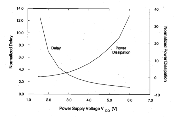
Fig 7 Normalized propagation delay and average switching power dissipation of a CMOS inverter, as a function of the power supply voltage VDD.
Notice that the dependence of circuit speed on the power supply voltage may also influence the relationship between the dynamic power dissipation and the supply voltage. However, this interpretation assumes that the switching frequency (i.e., the number of switching events per unit time) remains constant. If the circuit is always operated at the maximum frequency allowed by its propagation delay, the number of switching events per unit time (i.e., the operating frequency) will drop as the propagation delay becomes larger with the reduction of the power supply voltage. The net result is that the dependence of switching power dissipation on the power supply voltage becomes stronger than a simple quadratic relationship, shown in Figure above.
The propagation delay expressions above show that the negative effect of reducing the power supply voltage upon delay can be compensated for, if the threshold voltage of the transistors (VT) is scaled down accordingly. However, this approach is limited because the threshold voltage may not be scaled to the same extent as the supply voltage. When scaled linearly, reduced threshold voltages allow the circuit to produce the same speed-performance at a lower VDD. Figure below shows the variation of the propagation delay of a CMOS inverter as a function of the power supply voltage, and for different threshold voltage values.
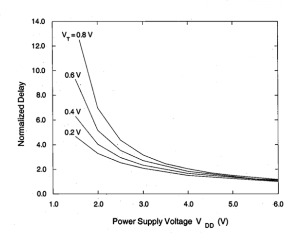
Fig 8 Variation of the normalized propagation delay of a CMOS inverter, as a function of the power supply voltage VDD and the threshold voltage VT.
We can see, for example, that reducing the threshold voltage from 0.8 V to 0.2 V can improve the delay at VDD= 2 V by a factor of 2. The positive influence of threshold voltage reduction upon propagation delay is especially pronounced at low power supply voltages, for VDD < 2 V. It should be noted, however, that using low- VT transistors raise significant concerns about noise margins and subthreshold conduction. Smaller threshold voltages lead to smaller noise margins for the CMOS logic gates. The subthreshold conduction current also sets a severe limitation against reducing the threshold voltage. For threshold voltages smaller than 0.2 V, leakage due to subthreshold conduction in stand-by, i.e., when the gate is not switching, may become a very significant component of the overall power consumption. In addition, propagation.
Variable-Threshold CMOS (VTCMOS) Circuits
We have seen that using a low supply voltage (VDD) and a low threshold voltage (VT) in CMOS logic circuits is an efficient method for reducing the overall power dissipation, while maintaining high speed performance. Yet designing a CMOS logic gate entirely with low-VT transistors will inevitably lead to increased subthreshold leakage, and consequently, to higher stand-by power dissipation when the output is not switching. One possible way to overcome this problem is to adjust the threshold voltages of the transistors in order to avoid leakage in the stand-by mode, by changing the substrate bias. The threshold voltage VT of an MOS transistor is a function of its source-to-substrate voltage VSB. In conventional CMOS logic circuits, the substrate terminals of all nMOS transistors are connected to ground potential, while the substrate terminals of all pMOS transistors are connected to VDD. This ensures that the source and drain diffusion regions always remain reverse-biased with respect to the substrate, and that the threshold voltages of the transistors are not significantly influenced by the body (back gate-bias) effect. In VTCMOS circuit technique, on the other hand, the transistors are designed inherently with a low threshold voltage, and the substrate bias voltages of nMOS and pMOS transistors are generated by a variable substrate bias control circuit, as shown in Figure below.
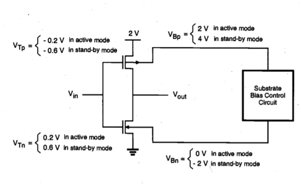
Fig.9 A variable-threshold CMOS (VTCMOS) inverter circuit. The threshold voltages of nMOS and pMOS transistors are increased by adjusting the substrate bias voltage, in order to reduce subthreshold leakage currents in the stand-by mode.
When the inverter circuit in Figure above is operating in its active mode, the substrate bias voltage of the nMOS transistor is VOn = 0 and the substrate bias voltage of the pMOS transistor is VBP = VDD. Thus, the inverter transistors do not experience any back gate-bias effect. The circuit operates with low VDD and low VT, benefiting from both low power dissipation (due to low VDD) and high switching speed (due to low VT). When the inverter circuit is in the stand-by mode, however, the substrate bias control circuit generates a lower substrate bias voltage for the nMOS transistor and a higher substrate bias voltage for the pMOS transistor.
As a result, the magnitudes of the threshold voltages VTl and VT, both increase in the stand-by mode, due to the back gate bias effect. Since the subthreshold leakage current drops exponentially with increasing threshold voltage, the leakage power dissipation in the stand-by mode can be significantly reduced with this technique. The VTCMOS technique can also be used to automatically control the threshold voltages of the transistors in order to reduce leakage currents, and to compensate for process-related fluctuations of the threshold voltages.
This approach is also called the Self-Adjusting Threshold-Voltage Scheme (SATS). The variable-threshold CMOS circuit design techniques are very effective for reducing the subthreshold leakage currents and for controlling threshold voltage values in low VDD - low VT applications. However, this technique usually requires twin-well or triple-well CMOS technology in order to apply different substrate bias voltages to different parts of the chip. Also, separate power pins may be required if the substrate bias voltage levels are not generated on-chip. The additional area occupied by the substrate bias control circuitry is usually negligible compared to the overall chip area.
Multiple-Threshold CMOS (MTCMOS) Circuits
Another technique which can be applied for reducing leakage currents in low voltage circuits in the stand-by mode is based on using two different types of transistors (both nMOS and pMOS) with two different threshold voltages in the circuit. Here, low-VT transistors are typically used to design the logic gates where switching speed is essential, whereas high- VT transistors are used to effectively isolate the logic gates in stand-by and to prevent leakage dissipation. The generic circuit structure of the MTCMOS logic gate is shown in Figure below.
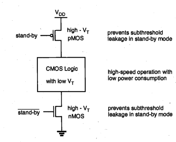
Fig.10 Generic structure of a multiple-threshold CMOS (MTCMOS) logic gate
In the active mode, the high-VT transistors are turned on and the logic gates consisting of low-VT transistors can operate with low switching power dissipation and small propagation delay. When the circuit is driven into stand-by mode, on the other hand, the high-VT transistors are turned off and the conduction paths for any subthreshold leakage currents that may originate from the internal low-VT circuitry are effectively cut off. Figure below shows a simple D-latch circuit designed with the MTCMOS technique. Note that the critical signal propagation path from the input to the output consists exclusively of low VT transistors, while a cross-coupled inverter pair consisting of high- VT transistors is used for preserving the data in the stand-by mode.
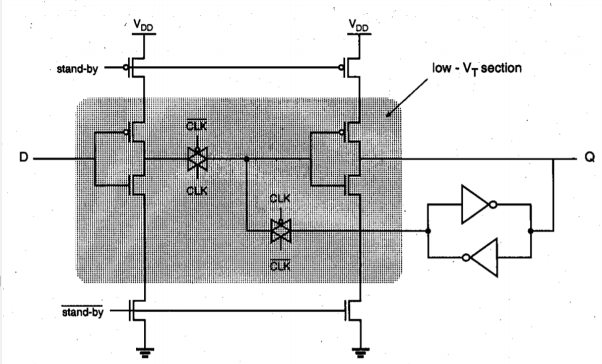
Fig 11 Low-power/low-voltage D-latch circuit designed with MTCMOS technique
The MTCMOS technique is conceptually easier to apply and to use compared to the VTCMOS technique, which usually requires a sophisticated substrate bias control mechanism. It does not require a twin-well or triple-well CMOS process; the only significant process-related overhead of MTCMOS circuits is the fabrication of MOS transistors with different threshold voltages on the same chip.
One of the disadvantages of the MTCMOS circuit technique is the presence of series-connected stand-by transistors, which increase the overall circuit area and also add extra parasitic capacitance. While the VTCMOS and MTCMOS circuit techniques can be very effective in designing low-power/low-voltage logic gates, they may not be used as a universal solution to low-power CMOS logic design. In certain types of applications where variable threshold voltages and multiple threshold voltages are infeasible due to technological limitations, system-level architectural measures such as pipelining and hardware replication techniques offer feasible alternatives for maintaining the system performance (throughput) despite voltage scaling.
Pipelining Approach
First, consider the single functional block shown in Figure below which implements a logic function F(INPUT) of the input vector, INPUT. Both the input and the output vectors are sampled through register arrays, driven by a clock signal CLK. Assume that the critical path in this logic block (at a power supply voltage of VDD) allows a maximum sampling frequency of fCLK; in other words, the maximum input-to-output propagation delay  max of this logic block is equal to or less than TCLK = l/fCLK. Figure below also shows simplified timing diagram of the circuit. A new input vector is latched into the input register array at each clock cycle, and the output data becomes valid with a latency of one cycle.
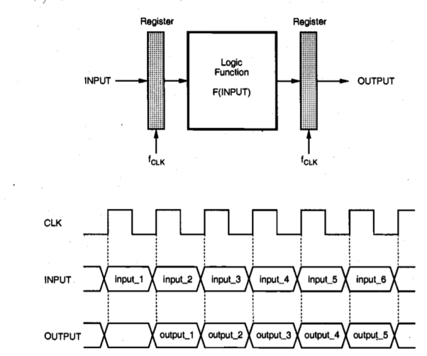
Fig 12 Single-stage implementation of a logic function and its simplified timing diagram.
Let Ctotal be the total capacitance switched every clock cycle. Here, Ctota, consists of (i) the capacitance switched in the input register array, (ii) the capacitance switched to implement the logic function, and (iii) the capacitance switched in the output register array. Then, the dynamic power consumption of this structure can be found as

Now consider an N-stage pipelined structure for implementing the same logic function, as shown in Figure below. The logic function F(INPUT) has been partitioned into N successive stages, and a total of (N- 1) register arrays have been introduced, in addition to the original input and output registers, to create the pipeline. All registers are clocked at the original sample rate, fCLK. If all stages of the partitioned function have approximately equal delays of

Then the logic blocks between two successive registers can operate N-times slower while maintaining the same functional throughput as before. This implies that the power supply voltage can be reduced to a value of VDD fnew' to effectively slow down the circuit by a factor of N.
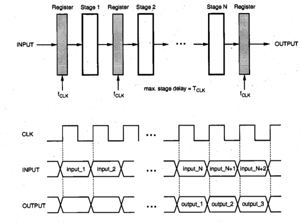
Fig 13 N-stage pipeline structure realizing the same logic function as in Figure above. The maximum pipeline stage delay is equal to the clock period, and the latency is N clock cycles.
The dynamic power consumption of the N-stage pipelined structure with a lower supply voltage and with the same functional throughput as the single-stage structure can be approximated by

Where Creg represents the capacitance switched by each pipeline register. Then, the power reduction factor achieved in a N-stage pipeline structure is

Parallel Processing Approach
Another method for trading off area for lower power dissipation is to use parallelism, or hardware replication. This approach could be useful especially when the logic function to be implemented is not suitable for pipelining. Consider N identical processing elements, each implementing the logic function F(INPUT) in parallel, as shown in Figure below. Assume that the consecutive input vectors arrive at the same rate as in the single stage case examined earlier. The input vectors are routed to all the registers of the N
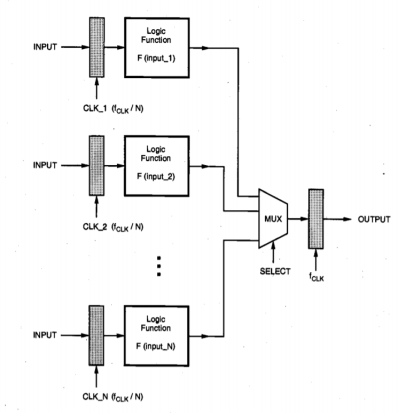
Fig 14 N-block parallel structure realizing the same logic function.
Notice the input registers are clocked at a lower frequency of (fcL / N). Processing blocks. Gated clock signals, each with a clock period of (N TCLK), are used to load each register every N clock cycles. This means that the clock signals to each input register are skewed by TCLK, such that each one of the N consecutive input vectors is loaded into a different input register. Since each input register is clocked at a lower frequency of (VCLK I N), the time allowed to compute the function for each input vector is increased by a factor of N. This implies that the power supply voltage can be reduced until the critical path delay equals the, new clock period of (N TCLK). The outputs of the N processing blocks are multiplexed and sent to an output register which operates at a clock frequency of fCLK' ensuring the same data throughput rate as before. The timing diagram of this parallel arrangement is given in Figure below.
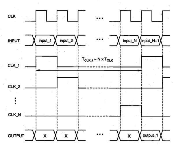
Fig 15 Simplified timing diagram of the N-block parallel structure
Since the time allowed to compute the function for each input vector is increased by a factor of N, the power supply voltage can be reduced to a value of VDD,new to effectively slow down the circuit. The total dynamic power dissipation of the parallel structure (neglecting the dissipation of the multiplexor) is found as the sum of the power dissipated by the input registers and the logic blocks operating at a clock frequency of (fCLK, N), and the output register operating at a clock frequency of fCLK.


Note that there is also an additional overhead which consists of the input routing capacitance, the output routing capacitance and the capacitance of the output multiplexor structure, all of which are increasing functions of N. If this overhead is neglected, the amount of power reduction achievable in a N-block parallel implementation is

The lower bound of switching power reduction realizable with architecture-driven voltage scaling is found, assuming zero threshold voltage, as

Key takeaway
For Pipelining approach, the architectural modification described here has a relatively small area overhead. A total of (N-1) register arrays have to be added to convert the original single-stage structure into a pipeline. While trading off area for lower power, this approach also increases the latency from one to N clock cycles. Yet in many applications such as signal processing and data encoding, latency is not a very significant concern.
Another approach to low power design is to reduce the switching activity and the amount of the switched capacitance to the minimum level required to perform a given task. The measures to accomplish this goal can range from optimization of algorithms to logic design, and finally to physical mask design. In the following, we will examine the concept of switching activity, and introduce some of the approaches used to reduce it.
The Concept of Switching Activity
The parameter  T also called the switching activity factor, depends on the Boolean function performed by the gate, the logic family, and the input signal statistics. First, we introduce two signal probabilities, PO and PI. PO corresponds to the probability of having a logic "0" at the output, and P1 = (1 - PO) corresponds to the probability of having a logic "1" at the output. Therefore, the probability that a power consuming (0-to- 1) transition occurs at the output node is the product of these two output signal probabilities. Consider, for example, a static CMOS NOR2 gate. If the two inputs are independent and uniformly distributed, the four possible input combinations (00, 01, 10, 11) are equally likely to occur. Thus, we can find from the truth table of the NOR2 gate that PO = 3/4, and P1= 1/4. The probability that a power-consuming transition occurs at the output node is therefore

The transition probabilities can be shown on a state transition diagram which consists of the two possible output states and the possible transitions among them as shown in below figure. In the general case of a CMOS logic gate with n input variables, the probability of a power consuming output transition can be expressed as a function of no, which is the number of zeros in the output column of the truth table.

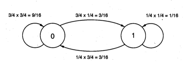
Fig 16 State transition diagram and state transition probabilities of a NOR2 gate.
The output transition probability is shown as a function of the number of inputs in Figure below, for different types of logic gates for equal input probabilities. For NAND or NOR gate, the truth table contains only one "0" or "1", respectively, regardless of the number of inputs. Therefore, the output transition probability drops as the number of inputs is increased. In XOR gate, on the other hand, the truth table always contains an equal number of logic "0" and logic " 1 " values. The output transition probability therefore remains constant at 0.25. In multi-level logic circuits, the distribution of input signal probabilities is typically not uniform, i.e., one cannot expect to have equal probabilities for the occurrence of a logic "0" and a logic " 1 ".
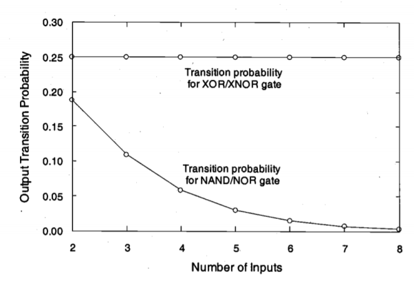
Fig.17 Output transition probabilities of different logic gates, as a function of the number of inputs.
Then, the output transition probability becomes a function of the input probability distributions. As an example, consider the NOR2 gate examined above. Let P1, A represent the probability of having a logic " 1 " at the input A, and PIB represent the probability of having a logic " 1 " at the input B. The probability of obtaining a logic " 1 " at the output node is

Using this expression, the probability of a power-consuming output transition is found as a function of P1, A and P1, B


Reduction of Switching Activity
Switching activity in CMOS digital integrated circuits can be reduced by algorithmic optimization, by architecture optimization, by proper choice of logic topology or by circuit-level optimization. In the following, we will briefly discuss some of the measures that can be applied to optimize the switching probabilities, and hence the dynamic power consumption. Algorithmic optimization depends heavily on the application and on the characteristics of the data such as dynamic range, correlation, and statistics of data transmission.
Some of the techniques can be applied only for specific applications such as Digital Signal Processing (DSP) and cannot be used for general purpose processing. For example, choosing a proper vector quantization (VQ) algorithm can be chosen for minimum switching activity. Also, the number of memory accesses, the number of multiplications and the number of additions can be reduced by about a factor of 30 if differential tree search algorithm is used instead of the full search algorithm.
The representation of data can have a significant impact on switching activity at the system level. In applications where data bits change sequentially and are highly correlated (such as the address bits to access instructions), the use of Gray coding leads to a reduced number of transitions compared to simple binary coding. Another example is the use of sign-magnitude representation instead of the conventional two's complement representation for signed data. A change in sign will cause transitions of the higher-order bits in the two's complement representation, whereas only the sign bit will change in sign magnitude representation. Therefore, the switching activity can be reduced by using the sign-magnitude representation in applications where the data sign changes are frequent.
Glitch Reduction
An important architecture-level measure to reduce switching activity is based on delay balancing and the reduction of glitches. In multi-level logic circuits, the propagation delay from one logic block to the next can cause spurious signal transitions, or glitches as a result of critical races or dynamic hazards. In general, if all input signals of a gate change simultaneously, no glitching occurs. But a dynamic hazard or glitch can occur if input signals change at different times. Thus, a node can exhibit multiple transitions in a single clock cycle before settling to the correct logic level as shown below. In some cases, the signal glitches are only partial, i.e., the node voltage does not make a full transition between the ground and VDD levels, yet even partial glitches can have a significant contribution to dynamic power dissipation.

Fig 18 Signal glitching in multi-level static CMOS circuits
Glitches occur primarily due to a mismatch or imbalance in the path lengths in the logic network. Such a mismatch in path lengths results in a mismatch of signal timing with respect to the primary inputs. As an example, consider the simple parity network shown below

Fig.19 (a) Implementation of a four-input parity (XOR) function using a chain structure. (b) Implementation of the same function using a tree structure which will reduce glitching transitions
If all XOR gates have the same delay and four input signals arrive at the same time, the network in Fig.19(a) will suffer from glitching due to the wide disparity between the arrival times of the input signals. In the network shown in Fig.19(b), on the other hand, all input arrival times are uniformly identical because the delay paths are balanced. Such redesign can significantly reduce the glitches, and consequently, the dynamic power dissipation in complex multi-level networks. Also notice that the tree structure shown in Fig.19(b) results in smaller overall propagation delay. Finally, it should be noted that glitching is not a significant issue in multi-level dynamic CMOS logic circuits, since each node undergoes at most one transition per clock cycle.
Gated Clock Signals
Another effective design technique for reducing the switching activity in CMOS logic circuits is the use of conditional, or gated clock signals. We have already seen that the switching power dissipation in the clock distribution network can be very significant. If certain logic blocks in a system are not immediately used during the current clock cycle, temporarily disabling the clock signals of these blocks will obviously save switching power that is otherwise wasted. Note that the design of an effective clock gating strategy requires careful analysis of the signal flow and of the interrelations among the various operations performed by the circuit. Figure below shows the block diagram of an N-bit number comparator circuit which is designed using the gated clock technique.
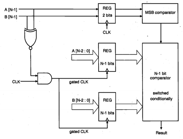
Fig 20 Block diagram of an N-bit number comparator with gated clock scheme.
The circuit compares the magnitudes of two unsigned N-bit binary numbers (A and B) and produces an output to indicate which one is larger. In the conventional approach, all input bits are first latched into two N-bit registers, and subsequently applied to the comparator circuit. In this case, two N-bit register arrays dissipate power in every clock cycle. Yet if the most significant bits, A [N-1 I and B[N-1], of the two binary numbers are different from each other, then the decision can be made by comparing the most significant bits (MSBs) only. The circuit shown in Figure above exploits this simple strategy for saving switching power which would otherwise be wasted to latch and to process the lower-order bits.
The two MSBs are latched in a two-bit register which is driven by the original system clock. At the same time, these two bits are applied to an XNOR gate and the output of the XNOR is used to generate the gated clock signal with an AND gate. If the two MSBs are different (i.e., "01" or "10"), the XNOR produces a logic "0" at the output, disabling the clock signal of the lower-order registers. In this case, a separate MSB comparator circuit is used to decide which one of the two numbers is larger. If the two MSBs are identical (i.e., "00" or " 11"), the gated clock signal is applied to the lower order registers and the decision is made by the (N- 1)-bit comparator circuit. The amount of power dissipated in the lower-order registers and the (N-1)-bit comparator circuit can be quite significant, especially if the bit-length (N) is large. Assuming that the incoming binary numbers are randomly distributed, we can see that the gated clock strategy effectively reduces the overall switching power dissipation of the system by approximately 50%, since a large portion of the system is disabled for half of all input combinations. This example shows that the gated clock strategy can be very effective for reducing switching power dissipation in certain logic circuits.
Key takeaway
In dynamic CMOS logic circuits, the output node is precharged during every clock cycle. If the output node was discharged (i.e., if the output value was equal to "0") in the previous cycle, the pMOS precharge transistor will draw a current from the power supply during the precharge phase. This means that the dynamic CMOS logic gate will consume power every time the output value equals "0", regardless of the preceding or following values.
Therefore, the power consumption of dynamic logic gates is determined by the signal-value probability of the output node and not by the transition probability. From the discussion above, we can see that signal-value probabilities are always larger than transition probabilities, hence, the power consumption of dynamic CMOS logic gates is typically larger than static CMOS gates under the same conditions.
Reduction of Switched Capacitance
System-Level Measures
At the system level, one approach to reduce the switched capacitance is to limit the use of shared resources. A simple example is the use of a global bus structure for data transmission between a large number of operational modules (Figure below). If a single shared bus is connected to all modules as in Figure (a), this structure results in a large bus capacitance due to (i) the large number of drivers and receivers sharing the same transmission medium, and (ii) the parasitic capacitance of the long bus line. Obviously, driving the large bus capacitance will require a significant amount of power consumption during each bus access. Alternatively, the global bus structure can be partitioned into a number of smaller dedicated local buses to handle the data transmission between neighboring modules, as shown in Figure (b). In this case, the switched capacitance during each bus access is significantly reduced, although multiple buses may increase the overall routing area on the chip.
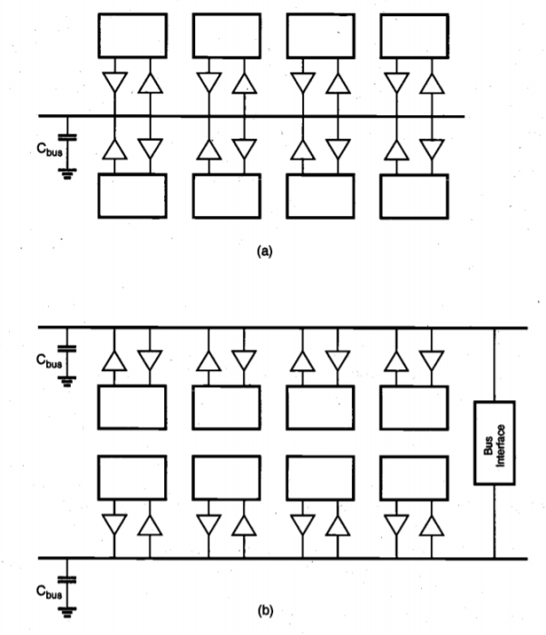
Fig 21(a) Using a single global bus structure for connecting a large number of modules on chip results in large bus capacitance and large dynamic power dissipation. (b) Using smaller local buses reduces the amount of switched capacitance, at the expense of additional chip area.
Circuit-Level Measures
The type of logic style used to implement a digital circuit also affects the output load capacitance of the circuit. The capacitance is a function of the number of transistors that are required to implement a given function. For example, one approach to reduce the load capacitance is to use transfer gates (pass-transistor logic) instead of conventional CMOS logic gates to implement logic functions. Pass-gate logic design is attractive since fewer transistors are required for certain functions such as XOR and XNOR. Therefore, this design style has emerged as a promising alternative to conventional CMOS, for low power design. Still, a number of important issues must be considered for pass-gate logic.
The threshold-voltage drop through nMOS transistors while transmitting a logic " 1 " makes swing restoration necessary in order to avoid static currents in subsequent inverter stages or logic gates. In order to provide acceptable output driving capabilities, inverters are usually attached to pass-gate outputs, which increases the overall area, time delay and the switching power dissipation of the logic gate. Because pass-transistor structures typically require complementary control signals, dual-rail logic is used to provide all signals in complementary form. As a consequence, two complementary nMOS pass-transistor networks are necessary in addition to swing restoration and output buffering circuitry, effectively diminishing the inherent advantages of pass transistor logic over conventional CMOS logic. Thus, the use of pass-transistor logic gates to achieve low power dissipation must be carefully considered, and the choice of logic design style must ultimately be based on a detailed comparison of all design aspects such as silicon area, overall delay as well as switching power dissipation.
Mask-Level Measures
The amount of parasitic capacitance that is switched (i.e., charged up or charged down) during operation can be also reduced at the physical design level, or mask level. The parasitic gate and diffusion capacitances of MOS transistors in the circuit typically constitute a significant amount of the total capacitance in a combinational logic circuit. Hence, a simple mask-level measure to reduce power dissipation is keeping the transistors (especially the drain and source regions) at minimum dimensions whenever possible and feasible, thereby minimizing the parasitic capacitances. Designing a logic gate with minimum-size transistors certainly affects the dynamic performance of the circuit, and this trade-off between dynamic performance and power dissipation should be carefully considered in critical circuits. Especially in circuits driving a large extrinsic capacitive load, e.g., large fan-out or routing capacitances, the transistors must be designed with larger dimensions. Yet in many other cases where the load capacitance of a gate. Is mainly intrinsic, the transistor sizes can be kept at a minimum. Note that most standard cell libraries are designed with larger transistors in order to accommodate a wide range of capacitive loads and performance requirements. Consequently, a standard-cell based design may have considerable overhead in terms of switched capacitance in each cell.
Adiabatic Logic Circuits
In conventional level-restoring CMOS logic circuits with rail-to-rail output voltage swing, each switching event causes an energy transfer from the power supply to the output node, or from the output node to the ground. During a O-to-VDD transition of the output, the total output charge Q = Cload VDD is drawn from the power supply at a constant voltage. Thus, an energy of EsuppIy = Cload VDD2 is drawn from the power supply during this transition. Charging the output node capacitance to the voltage level VDD means that at the end of the transition, the amount of stored energy in the output node is Estored = Cload VDD2/2. Thus, half of the injected energy from the power supply is dissipated in the pMOS network while only one half is delivered to the output node. During a subsequent VDD to-O transition of the output node, no charge is drawn from the power supply and the energy stored in the load capacitance is dissipated in the nMOS network.
To increase the energy efficiency of logic circuits, other measures can be introduced for recycling the energy drawn from the power supply. A novel class of logic circuits called adiabatic logic offers the possibility of further reducing the energy dissipated during switching events, and the possibility of recycling, or reusing, some of the energy drawn from the power supply. To accomplish this goal, the circuit topology and the operation principles have to be modified, sometimes drastically. The amount of energy recycling achievable using adiabatic techniques is also determined by the fabrication technology, switching speed and voltage swing.
Adiabatic Switching
Consider the simple circuit shown in Figure below where a load capacitance is charged by a constant current source. This circuit is similar to the equivalent circuit used to model the charge-up event in conventional CMOS circuits, with the exception that in conventional digital CMOS circuits, the output capacitance is charged by a constant voltage source and not by a constant current source. Here, R represents the on-resistance of the pMOS network. Also note that a constant charging current corresponds to a linear voltage ramp. Assuming that the capacitance voltage VC is zero initially, the variation of the voltage as a function of time can be found as

Hence, the charging current can be expressed as a simple function of Vc and time t.

The amount of energy dissipated in the resistor R from t = 0 to t = T can be found as

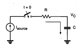
Fig 22 Constant-current source charging a load capacitance C, through a resistance R.
The dissipated energy during this charge-up transition can also be expressed as follows.

First, the dissipated energy is smaller than for the conventional case if the charging time T is larger than 2 RC. In fact, the dissipated energy can be made arbitrarily small by increasing the charging time, since Ediss is inversely proportional to T. Also, we observe that the dissipated energy is proportional to the resistance R, as opposed to the conventional case where the dissipation depends on the capacitance and the voltage swing. Reducing the on-resistance of the pMOS network will reduce the energy dissipation. We have seen that the constant-current charging process efficiently transfers energy from the power supply to the load capacitance.
A portion of the energy thus stored in the capacitance can also be reclaimed by reversing the current source direction, allowing the charge to be transferred from the capacitance back into the supply. This possibility is unique to the adiabatic operation, since in conventional CMOS circuits the energy is dissipated after being used only once. The constant-current power supply must certainly be capable of retrieving the energy back from the circuit. Adiabatic logic circuits thus require non-standard power supplies with time-varying voltage, also called pulsed power supplies. The additional hardware overhead associated with these specific power supply circuits is one of the design trade-off that must be considered when using the adiabatic logic.
Adiabatic Logic Gates
In the following, we will examine simple circuit configurations which can be used for adiabatic switching. Note that most of the research on adiabatic logic circuits are rather recent. Therefore, the circuits presented here should be considered as simple examples. Other circuit topologies are also possible, but the overall theme of energy recycling should be enforced, regardless of specific circuit configuration.
First, consider the adiabatic amplifier circuit shown in Figure below, which can be used to drive capacitive loads. It consists of two CMOS transmission gates and two nMOS clamp transistors. Both the input (X) and the output (Y) are dual-rail encoded, which means that the inverses of both signals are also available, to control the CMOS transmission gates.
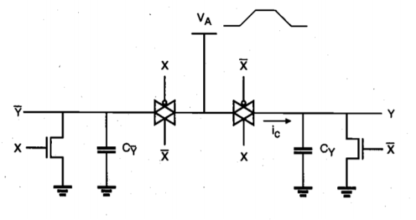
Fig 23 Adiabatic amplifier circuit which transfers the complementary input signals to its complementary outputs through CMOS transmission gates.
When the input signal X is set to a valid value, one of the two transmission gates becomes transparent. Next, the amplifier is energized by applying a slow voltage ramp VA, rising from zero to VDD. The load capacitance at one of the two complementary outputs is adiabatically charged to VDD through the transmission gate, while the other output node remains clamped to ground potential. When the charging process is completed, the output signal pair is valid and can be used as an input to other similar circuits. Next, the circuit is de-energized by ramping the voltage VA back to zero. Thus, the energy that was stored in the output load capacitance is retrieved by the power supply. Note that the input signal pair must be valid and stable throughout this sequence. The simple circuit principle of the adiabatic amplifier can be extended to allow the implementation of arbitrary logic functions.
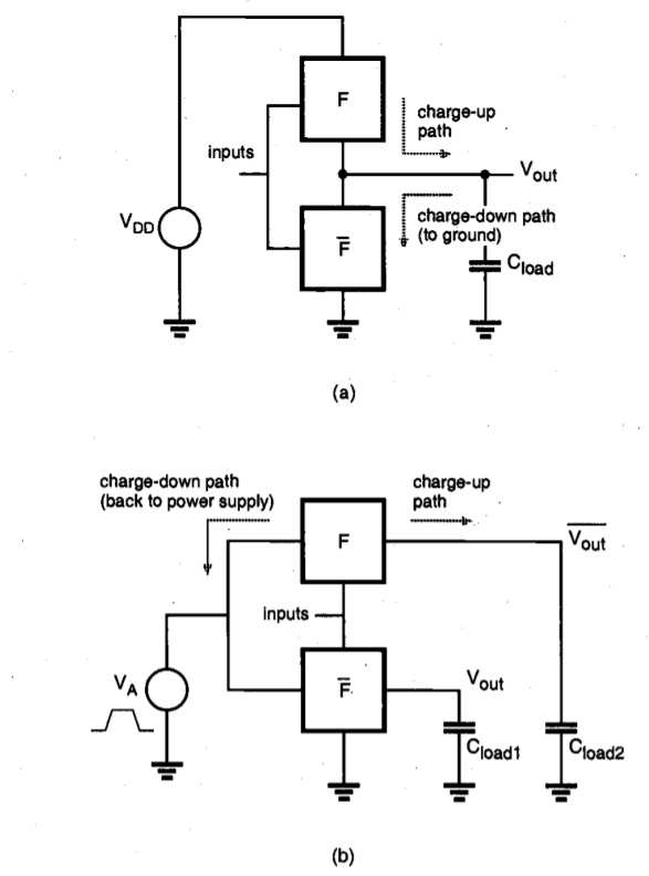 Fig 24(a) The general circuit topology of a conventional CMOS logic gate. (b) The topology of an adiabatic logic gate implementing the same function.
The simple circuit principle of the adiabatic amplifier can be extended to allow the implementation of arbitrary logic functions. Figure below shows a general circuit topology for conventional CMOS logic gates and adiabatic counterparts. To convert a conventional CMOS logic gate into an adiabatic gate, the pull-up and pull-down networks must be replaced with complementary transmission-gate (T-gate) networks. The T-gate network implementing the pull-up function is used to drive the true output of the adiabatic gate, while the T-gate network implementing the pull-down function drives the complementary output node. Note that all inputs should also be available in complementary form. Both networks in the adiabatic logic circuit are used to charge-up as well as charge-down the output capacitances, which ensures that the energy stored at the output node can be retrieved by the power supply, at the end of each cycle. To allow adiabatic operation, the DC voltage source of the original circuit must be replaced by a pulsed-power supply with ramped voltage output. Note that the circuit modifications which are necessary to convert a conventional CMOS logic circuit into an adiabatic logic circuit increase the device count by a factor of two or even more. In general, the reduction of energy dissipation comes at the cost of slower switching speed, a trade-off in all adiabatic methods.
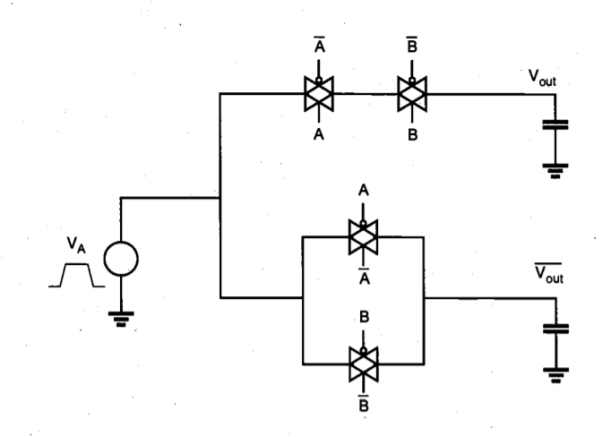
Fig 25 Circuit diagram of an adiabatic CMOS AND/NAND gate
Stepwise Charging Circuits
We have seen earlier that the dissipation during a charge-up event can be minimized, and in the ideal case it can be reduced to zero by using a constant-current power supply. This requires that the power supply be able to generate linear voltage ramps. Practical supplies can be constructed by using resonant inductor circuits to approximate the constant output current and the linear voltage ramps with sinusoidal signals. But the use of inductors presents several difficulties at the circuit level, especially in view of chip-level integration and overall efficiency. An alternative to using pure voltage ramps is to use stepwise supply voltage waveforms, where the output voltage of the power supply is increased and decreased in small increments during charging and discharging. Since the energy dissipation depends on the average voltage drop traversed by the charge that flows onto the load capacitance, using smaller voltage steps, or increments, should reduce the dissipation considerably.
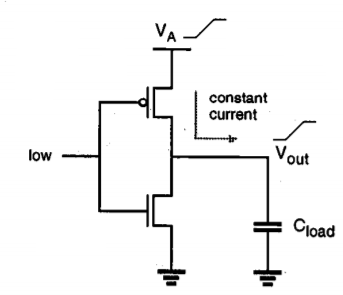
Fig.26 A CMOS inverter circuit with a stepwise-increasing supply voltage.
Figure above shows a CMOS inverter driven by a stepwise supply voltage waveform. Assume that the output voltage is equal to zero initially. With the input voltage set to logic low level, the power supply voltage VA is increased from 0 to VDD, in n equal voltage steps (Figure below). Since the pMOS transistor is conducting during this transition, the output load capacitance will be charged up in a stepwise manner. The on-resistance of the pMOS transistor can be represented by the linear resistor R. Thus, the output load capacitance is being charged up through a resistor, in small voltage increments. For the i time increment, the amount of capacitor current can be expressed as

Solving the differential equation with initial conditions


Here N is the number of supply voltage waveform. The amount of energy dissipated during one voltage step increment can be given as

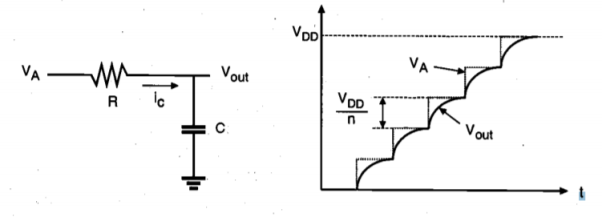
Fig 27 Equivalent circuit, and the input and output voltage waveforms of the CMOS inverter circuit
Since n steps are used to charge up the capacitance to VDD, the total dissipation is

According to this simplified analysis, charging the output capacitance with n voltage steps or increments reduces the energy dissipation per cycle by a factor of n. Therefore, the total power dissipation is also reduced by a factor of n using stepwise charging. This result implies that if the voltage steps can be made very small and the number of voltage steps n approaches infinity (i.e., if the supply voltage is a slow linear ramp), the energy dissipation will approach zero.
Key takeaway
The term "adiabatic" is typically used to describe thermodynamic processes that have no energy exchange with the environment, and therefore, no energy loss in the form of dissipated heat. In our case, the electric charge transfer between the nodes of a circuit will be viewed as the process, and various techniques will be explored to minimize the energy loss, or heat dissipation, during charge transfer events. It should be noted that fully adiabatic operation of a circuit is an ideal condition which may only be approached asymptotically as the switching process is slowed down. In practical cases, energy dissipation associated with a charge transfer event is usually composed of an adiabatic component and a non-adiabatic component. Therefore, reducing all energy loss to zero may not be possible, regardless of the switching speed
Need of Design for Testability (DFT)
- DFT is a technique, which facilitates a design to become testable after fabrication. Add on logic is added along with the design logic during implementation process helps in post-production testing.
- Post-production testing is necessary because, the process of manufacturing is not 100% error free.
- There are defects in silicon which contribute towards the errors introduced in the physical device.
- A chip will not work as per the specifications if there are any errors introduced in fabrication.
- All the functional tests run on each of a million physical devices, is very time consuming, there was a need for a method, which assures its maturity without running full exhaustive tests on the physical device in order to ensure that the device has been manufactured correctly.
Testability
- The increasing capability of fabricating a very large number of transistors on a single integrated-circuit chip and the complexity of the possible systems has increased the importance of being able to test such circuits in an acceptable way and in an acceptable time.
- The time difficulties of tests are primarily due to the limited number of I/O
- The connections on a chip are the only means of access to the circuit, the ratio of the number of gates on a chip to the number of accessible I/Os goes on increasing with chip size.
- To minimize the difficulties, present methods are adopted to make the problem manageable.
- This involves a consideration of the testability of the circuit at the design stage, with some partitioning and structured design methodology essential in the case of very complex circuits.
Types of faults
The various fault types are:
- Assertion Fault.
- Behavioral Fault.
- Branch Fault.
- Bridging (*)
- Bus Fault.
- Cross-point Fault.
- Defect-oriented Fault (physical level faults, bridging, stuck-open, IDDQ).
Fault models
A fault model is an engineering model that could go wrong in the construction or operation of a piece of equipment.
From the model, the designer or user can then predict the consequences of this particular fault.
Fault models can be used in almost all branches of engineering.
Basic fault models in digital circuits include:
- Static faults, which give incorrect values at any speed and sensitized by performing only one operation:
- The stuck-at fault model.
In this, a signal, or gate output, is stuck at a 0 or 1 value, independent of the inputs to the circuit.
- The bridging fault model.
Here, two signals are connected together when they should not be. Depending on the logic circuitry employed, this may result in a wired-OR or wired-AND logic function. Since there are O(n2) potential bridging faults, they are normally restricted to signals that are physically adjacent in the design.
- The transistor faults.
This model describes faults for CMOS logic gates. At transistor level, a transistor maybe stuck-short or stuck-open. In stuck-short, a transistor behaves as it is always conducting (or stuck-on), and stuck-open is when a transistor never conducts current (or stuck-off). Stuck-short will produce a short between VDD and VSS.
- The open fault model.
Here a wire is assumed broken, and one or more inputs are disconnected from the output that should drive them. As with bridging faults, the resulting behavior depends on the circuit implementation.
- Dynamic faults, only at-speed and are sensitized by performing multiple operations sequentially:
- The transition delay fault (or transition fault) model, where the signal eventually assumes the correct value, but more slowly (or rarely, more quickly) than normal.
- Small-delay-defect mode.
The controllability of a circuit is a measure of the ease (or difficulty) with which the controller (test engineer) can establish a specific signal value at each node by setting values at the circuit input terminals. The observability is a measure of the ease (or difficulty) with which one can determine the signal value at any logic node in the circuit by controlling its primary input and observing the primary output. Here the term primary refers to the I/O boundary of the circuit under test. The degree of controllability and observability and, thus, the degree of testability of a circuit, can be measured with respect to whether test vectors are generated deterministically or randomly. For example, if a logic node can be set to either logic 1 or 0 only through a very long sequence of random test vectors, the node is said to have a very low random controllability since the probability of generating such a vector in random test generation is very low.
There exist time constraints in practice, and in such cases the circuit may not be considered testable. There are deterministic procedures for test generation for combinational circuits, such as the D-algorithm which uses a recursive search procedure advancing one gate at a time and backtracking, if necessary, until all the faults are detected. The D-algorithm. Requires a large amount of computer time. To overcome such shortcomings, many improved algorithms such as Path-Oriented Decision Making (PODEM) and FAN-out-oriented test generation (FAN) have been introduced, Sequential circuit test generation is several orders of magnitude more difficult than these algorithms. To ease the task of ATG, design-for-test (DFT) techniques are routinely employed. Consider the simple circuit in Figure below consisting of four simple logic gates.
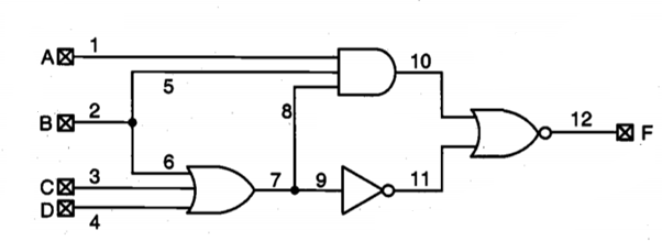
Fig 28 A simple circuit consisting of four gates with four primary inputs and one primary output.
To detect any defect on line 8, the primary inputs A and B must be set to logic 1. However, such a setting forces line 7 to logic 1. Thus, any stuck-at- (s-a- 1) fault on line 7 cannot be tested at the primary output, although in the absence of such a fault, the logic value on line 7 can be fully controllable through primary inputs B, C, and D. Therefore, this circuit is not fully testable. The main cause of this difficulty in this circuit is the fact that input B fans out to lines 5 and 6, and then after the OR3 gate, both line signals are combined in the AND3 gate. Such a fanout is called reconvergent fanout. Reconvergent fanouts make the testing of the circuit much more difficult.
If a large number of input vectors are required to set a particular node value to 1 or 0 (fault excitation) and to propagate an error at the node to an output (fault effect propagation), then the testability is low. The circuits with poor controllability include those with feedbacks, decoders, and clock generators. The circuits with poor observability include sequential circuits with long feedback loops and circuits with reconvergent fanouts, redundant nodes, and embedded memories such as RAM, ROM, and PLA.
Test engineers usually have to construct test vectors after the design is completed. This invariably requires a substantial amount of time and effort that could be avoided if testing is considered early in the design flow to make the design more testable. As a result, integration of design and test, referred to as design for testability (DFT), was proposed in the 1970s. To structurally test circuits, we need to control and observe logic values of internal lines. Unfortunately, some nodes in sequential circuits can be very difficult to control and observe; for example, activity on the most significant bit of an n bit counter can only be observed after 2"“' clock cycles. Testability measures of controllability and observability were first defined in the 1970s to help find those parts of a digital circuit that will be most difficult to test and to assist in test pattern generation for fault detection. Many DFT techniques have been proposed since that time. DFT techniques generally fall into one of the following three categories:
(1) Ad hoc DFT techniques
(2) Level-sensitive scan design (LSSD) or scan design
(3) Built-in self-test (BIST)
Ad hoc DFT Techniques
Ad hoc testing combines a collection of tricks and techniques that can be used to increase the observability and controllability of a design and that are generally applied in an application-dependent fashion. An example of such a technique is illustrated in Fig. (a), which shows a simple processor with its data memory. Under normal configuration, the memory is only accessible through the Processor. Writing and reading a data value into and out of a single memory position requires a number of clock cycles.
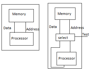
The controllability and observability of the memory can be dramatically improved by add multiplexers on the data and address buses (Fig.). During normal operation mode, these selectors direct the memory ports to the processor. During test, the data and address ports are connected directly to the I/O pins, and testing the memory can proceed more efficiently. The example illustrates some important design-for testability concepts.
It is often worthwhile to introduce extra hardware that has no functionality except improving the testability. Designers are often willing to incur a small penalty in area and performance if it makes the design substantially more observable or controllable. Design-for-testability often means that extra I/O pins must be provided besides die nominal functional I/O pins. The test port in Fig.(b) is such an extra pin. To reduce the number of extra pads that would be required, one can multiplex test signals and functional signals on the same pads. For example, the I/O bus in Fig. (b) serves as a data bus during normal operation and provides and collects the test patterns during testing.
An extensive collection of ad hoc test approaches has been devised. Examples include the partitioning of large state machines, addition of extra test points, prevision of reset states, and introduction of test buses. While very effective, the applicability of most of these techniques depends upon the application and architecture at hand. The insertion into a given Hating requires expert knowledge and is difficult to automate. Stricture and automatable approaches are more desirable.
Key takeaway
DFT techniques generally fall into one of the following three categories:
(1) Ad hoc DFT techniques
(2) Level-sensitive scan design (LSSD) or scan design
(3) Built-in self-test (BIST)
Objectives of Scan Design
- Scan design is implemented to provide controllability and observability of internal state variables for testing a circuit.
- It is also effective for circuit partitioning.
- A scan design with full controllability and observability turns the sequential test problem into a combinational one.
Scan Design Requirements
- Circuit is designed using pre-specified design rules. ƒ Test structure (hardware) is added to the verified design.
- One (or more) test control (TC) pin at the primary input is required.
- Flip-flops are replaced by scan flip-flops (SFF) and are connected so that they behave as a shift register in the test mode. The output of one SFF is connected to the input of next SFF. The input of the first flip-flop in the chain is directly connected to an input pin (denoted as SCANIn), and the output of the last flipflop is directly connected to an output pin (denoted as SCANOUT). In this way, all the flip-flops can be loaded with a known value, and their value can be easily accessed by shifting out the chain. Figure 39.1 shows a typical circuit after the scan insertion operation.
- Input/output of each scan shift register must be available on PI/PO.
- Combinational ATPG is used to obtain tests for all testable faults in the combinational logic.
- Shift register tests are e applied and ATPG tests are converted into scan sequences for use in manufacturing test.
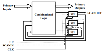
Fig 29 Scan structure to a design
Figure above shows a scan structure connected to design. The scan flip-flips (FFs) must be interconnected in a particular way. This approach effectively turns the sequential testing problem into a combinational one and can be fully tested by compact ATPG patterns. Unfortunately, there are two types of overheads associated with this technique that the designers care about very much. These are the hardware overhead (including three extra pins, multiplexers for all FFs, and extra routing area) and performance overhead (including multiplexer delay and FF delay due to extra load).
Scan Design Rules
- Only clocked D-type master-slave flip-flops for all state variables should be used.
- At least one PI pin must be available for test. It is better if more pins are available.
- All clock inputs to flip-flops must be controlled from primary inputs (PIs). There will be no gated clock. This is necessary for FFs to function as a scan register.
- Clocks must not feed data inputs of flip-flops. A violation of this can lead to a race condition in the normal mode.
Scan Overheads
- The use of scan design produces two types of overheads. These are area overhead and performance overhead. The scan hardware requires extra area and slows down the signals.
- IO pin overhead: At least one primary pin necessary for test.
- Area overhead: Gate overhead = [4 nsff/(ng+10nff)] x 100%, where ng = number of combinational gates; nff = number of flip-flops; nsff = number of scan flip-flops; For full scan number of scan flip-flops is equal to the number of original circuit flip-flops. Example: ng = 100k gates, nff = 2k flip-flops, overhead = 6.7%. For more accurate estimation scan wiring and layout area must be taken into consideration.
- Performance overhead: The multiplexer of the scan flip-flop adds two gate-delays in combinational path. Fanouts of the flip-flops also increased by 1, which can increase the clock period.
As the complexity of VLSI circuits increases, test generation and application become an expensive and not always very effective means of testing. Built-in Self-Test (BIST) is another solution.
It is a mechanism that permits a machine to test itself. Engineer’s design BISTs to meet requirements such as:
- High reliability
- Lower repair cycle times
Or constraints such as:
- Limited technician accessibility
- Cost of testing during manufacture
The main purpose of BIST is to reduce the complexity, and thereby decrease the cost and reduce reliance upon external (pattern-programmed) test equipment.
It reduces cost in two ways:
- Reduces test-cycle duration
- Reduces the complexity of the test/probe setup, by reducing the number of I/O signals that must be driven/examined under tester control.
Figure below shows the Built-in Self-Test system.
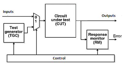
Figure 30. BIST
Advantages:
- Lower cost due to elimination of external tester
- In-system, at-system, high-quality testing
- Faster fault detection, ease of diagnosis
- Overcomes pin limitations and related interfacing problems
- Reduces maintenance and repair costs at system level.
References:
1. D. A. Pucknell and K. Eshraghian, “Basic VLSI Design: Systems and Circuits”, PHI, 3rd Ed.,1994.
2. W.Wolf, Modern VLSI Design: System on Chip, Third Edition, Pearson, 2002.